
Cryo-Focused Ion Beam-Induced Deposition of Tungsten–Carbon Nanostructures Using a Thermoelectric Plate


1
Instituto de Nanociencia y Materiales de Aragón (INMA), CSIC-Universidad de Zaragoza, 50009 Zaragoza, Spain
2
Departamento de Física de la Materia Condensada, Facultad de Ciencias, Universidad de Zaragoza, 50009 Zaragoza, Spain
3
Laboratorio de Microscopías Avanzadas (LMA), University of Zaragoza, 50018 Zaragoza, Spain
*
Author to whom correspondence should be addressed.
Appl. Sci. 2021, 11(21), 10123; https://doi.org/10.3390/app112110123
Submission received: 30 September 2021
/
Revised: 26 October 2021
/
Accepted: 26 October 2021
/
Published: 28 October 2021
(This article belongs to the Special Issue Nanoscale Assembly and Integration for Applications)
Abstract
:Focused Ion Beam-Induced Deposition (FIBID) is a single-step nanopatterning technique that applies a focused beam of ions to induce the decomposition of a gaseous precursor. The processing rate of FIBID increases by two orders of magnitude when the process is performed at cryogenic temperatures (Cryo-FIBID): the precursor forms a condensed layer on the surface of the cooled substrate, greatly enhancing the amount of material available for decomposition. Cryo-FIBID has been achieved so far by making use of liquid nitrogen-based cooling circuits, which require the passage of a flowing gas as a cooling agent. Here, the Cryo-FIBID of the W(CO) precursor is performed using a coolant-free thermoelectric plate utilizing the Peltier effect. Performed at −60 C, the procedure yields a W–C-based material with structural and electrical properties comparable to those of its counterpart grown in coolant-based Cryo-FIBID. The use of the thermoelectric plate significantly reduces the vibrations and sample drift induced by the flow of passing coolant gas and allows for the fabrication of similar nanostructures. In summary, the reported process represents a further step towards the practical implementation of the Cryo-FIBID technique, and it will facilitate its use by a broader research community.
1. Introduction
The research and development of improved and specialized nanofabrication procedures is a perennial need in both industry and research fields. One example of a relevant approach for the growth of nanostructures is Focused Ion Beam-Induced Deposition (FIBID), a direct-write single-step technique that exploits the interactions between a focused beam of charged ions and a substrate to induce the decomposition of a gaseous precursor material [1,2]. Relying on the direct deposition of the material via these interactions only, without the usage of resists or any other intermediate process, FIBID represents a highly flexible and reliable approach for the single-step patterning of different materials [3,4,5,6,7].
Conventional FIBID is performed by injecting a gaseous precursor material, containing the element of interest, in close proximity to a substrate. Precursor molecules adsorb on its top surface, constituting a molecular monolayer in dynamical equilibrium with the vacuum system of the instrument chamber. The beam is then scanned on the substrate, tracing a previously-defined pattern. The energy exchange between the ions in the beam and the molecules in the substrate results in the emission of secondary electrons (among other particles) near the point of irradiation, whose energy, when transferred to the adsorbed precursor molecules, induces their dissociation into volatile and non-volatile parts. The volatile parts are pumped away by the vacuum system of the instrument, while the non-volatile constituents permanently remain on top of the substrate, forming a deposit with a shape that follows the path traced by the beam.
One of the most significant drawbacks of this technique is its serial nature—in FIBID, the features to be grown are scanned sequentially and typically one at a time. Furthermore, structures grown by FIBID typically find their maximum size in the hundreds of m, with higher throughput techniques (e.g., optical [8] and electron-beam lithography [9]) being used for large-scale patterns.
The usage of FIBID is thus commonly limited to small features, due to the unfavorable throughput and the risk of the appearance of growth artifacts related to instrument strain over long operating times. It is not unusual for the exposed area to moderately drift in time scales of minutes (due to ambient noise or focused beam instability), which is usually negligible for short deposition times, but it can severely hinder the proper growth of larger features.
Very recently, the usage of FIBID under cryogenic conditions (Cryo-FIBID) was reported to yield an increase in the deposition processing time of two orders of magnitude [10]. By injecting the precursor with the substrate previously cooled below the condensation temperature of the precursor gas, a thick layer of condensed precursor forms on the substrate surface, providing a much larger amount of material available for decomposition than the gaseous molecular monolayer would. The precursor overabundance allows for the usage of reduced ion doses, which result in much shorter processing times [11]. A functionally similar approach that makes use of a focused beam of electrons instead of ions has also been successfully demonstrated in the growth of platinum [12,13] and copper [14] nanostructures.
The processing speed reportedly increases by two orders of magnitude for the Cryo-FIBID of nanostructures based on tungsten [10], platinum [15], and cobalt [16]. Combined with the fact that the ion interaction volume is mostly localized within the condensed layer, the low ion dose employed in Cryo-FIBID processes also effectively nullifies Ga implantation and substrate modification, both of which are unavoidable (and usually unwanted) features of conventional FIBID [17,18]. With the fundamentals of conventional FIBID remaining the same, Cryo-FIBID is still a serial deposition process, yet such a drastic increase in processing speed permits the growth of much larger features in a shorter time.
The aforementioned reports of Cryo-FIBID employ a liquid nitrogen-based cooling system to achieve the required low temperatures (in the order of −100 C). In such an approach, cooled gaseous nitrogen is made to flow through rubber tubes near the sample stage, cooling it down along with the sample. While effective for reaching the desired temperatures, the coolant flow introduces unavoidable vibrations in the sample, which, depending on the work dimensions and the required patterning resolution, can compromise the quality of the final deposit. The relatively high cost of a cryogenic module might also represent a deterrent for the technique.
In this work, a coolant-free approach to the Cryo-FIBID procedure for the deposition of W(CO) is presented. The control of the sample temperature is achieved using a commercial Peltier effect cooling stage, fundamentally consisting of a thermoelectric plate. This system does not require any cooling agents to operate and thus does not introduce the associated disturbances during growth. With a deposition temperature of −60 C (40 C above the previously reported value of −100 C using liquid nitrogen), tungsten–carbon nanostructures have been grown and characterized.
2. Materials and Methods
Si pieces with a 200 nm-thick thermally-grown SiO layer on top were used as substrates. A supporting Ti structure of contact pads, each 100 nm in thickness, was deposited in the pieces by optical lithography before the growth of the nanowires.
Both the fabrication and electrical characterization of the samples were performed with a Thermo Fisher Helios 650 NanoLab FIB/SEM microscope, fitted with a Ga ion column and a gas injection system (GIS) for the W(CO) precursor. The acceleration voltage, ion beam current, and dwell time were kept at 30 kV, 7.7 pA, and 200 ns, respectively, in all the growth processes.
Apart from the temperature, two operating parameters are fundamentally different in a Cryo-FIBID procedure when compared to conventional FIBID: the distance between the sample and the GIS nozzle from which the gaseous precursor is delivered, and the ion dose. The two are intertwined: on the one hand, the GIS–sample distance coarsely determines the amount of precursor that reaches the sample. In room-temperature FIBID, sub-mm distances are typically used to ensure that a continuously replenished precursor monolayer is maintained. Since in Cryo-FIBID precursor molecules reaching the substrate condensate on arrival, larger distances are used, typically in the 5–10 mm range. On the other hand, the ion dose required to decompose the condensed layer will in turn depend on the amount of precursor available, but this will in any case be much lower than its room-temperature counterpart. The GIS–sample distance was set at 10 and 7.5 mm, and the ion dose was modified in the 10–500 C/cm range.
To properly achieve the condensation of the precursor layer on top of the substrate, its delivery is performed in a different manner than that used in conventional FIBID: instead of continuously delivering the gaseous precursor to maintain the dynamical equilibrium in the adsorbed monolayer, the GIS nozzle is opened for a fixed amount of time of 10 s, during which the 20 nm-thick precursor condensed layer (estimated from FIB/SEM cross-sectioning of deposited material) forms as the gaseous molecules arrive to the cooled substrate, and is then closed during ion irradiation. The vacuum chamber of the FIB/SEM instrument was kept at a base pressure of mbar, which reached pressure values around mbar during the 10 s-long injection of the gaseous precursor into the chamber.
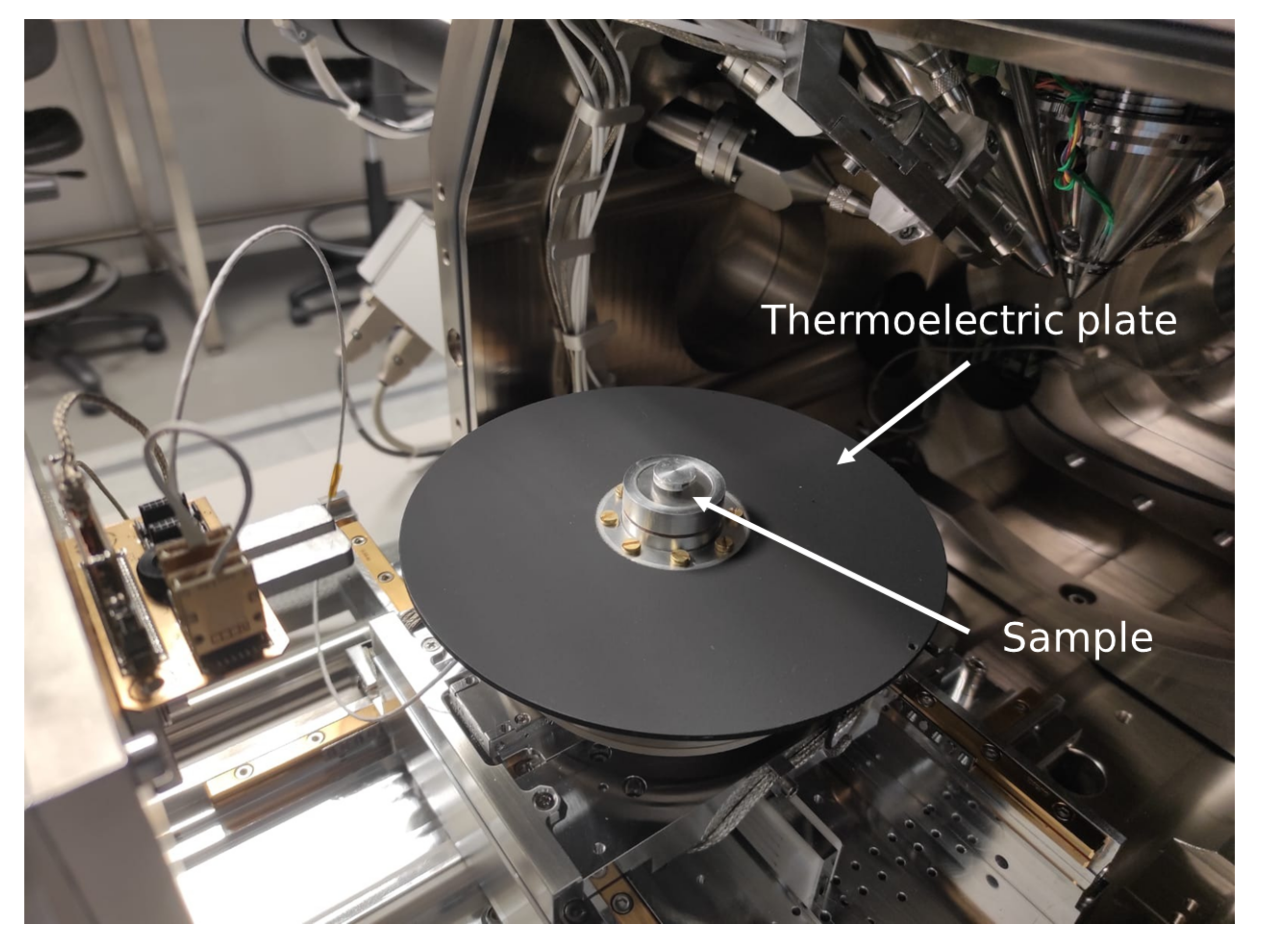
The sample temperature was controlled and regulated using a Kleindiek Nanotechnik Micro Heating Cooling Stage (MHCS) (Figure 1). For precursor delivery and deposition, the temperature of the stage was set at −60 C, which was reached after a 7 min-long cooling period. The sample was reheated to 20 C following a slower ramp of 5 C/min for 16 min, amounting to a total of 23 min for a complete cycle (the actual growth times are negligible, only consisting of the 10 s of GIS delivery and the s/ms-long exposures).
The composition of the samples was assessed by Energy Dispersive X-ray Spectroscopy (EDX), carried out in a commercial Thermo Fisher Inspect 50 Scanning Electron Microscope using an acceleration voltage of 5 kV. The electrical measurements were taken with a Kleindek Nanotechnik commercial microprobe station mounted on the FIB/SEM microscope, equipped with four microprobes and connected by a chamber feedthrough to a Keithley Instruments 6221 DC current source and 2182 A nanovoltmeter.
3. Results and Discussion
3.1. Growth
The capabilities of the technique were explored by simultaneously investigating the effect that the ion dose and GIS-sample distance have on the nature of the nanostructures. The ion dose D was calculated as the charge received per area, , where I is the ion beam current, t is the deposition time, and A is the area of the feature that is to be patterned. The parameter was therefore easy to tune experimentally by modifying the deposition time according to the dimensions of the pattern and the used ion beam current. The standard value of D in previously reported studies for Cryo-FIBID of W(CO) is 55 C/cm.
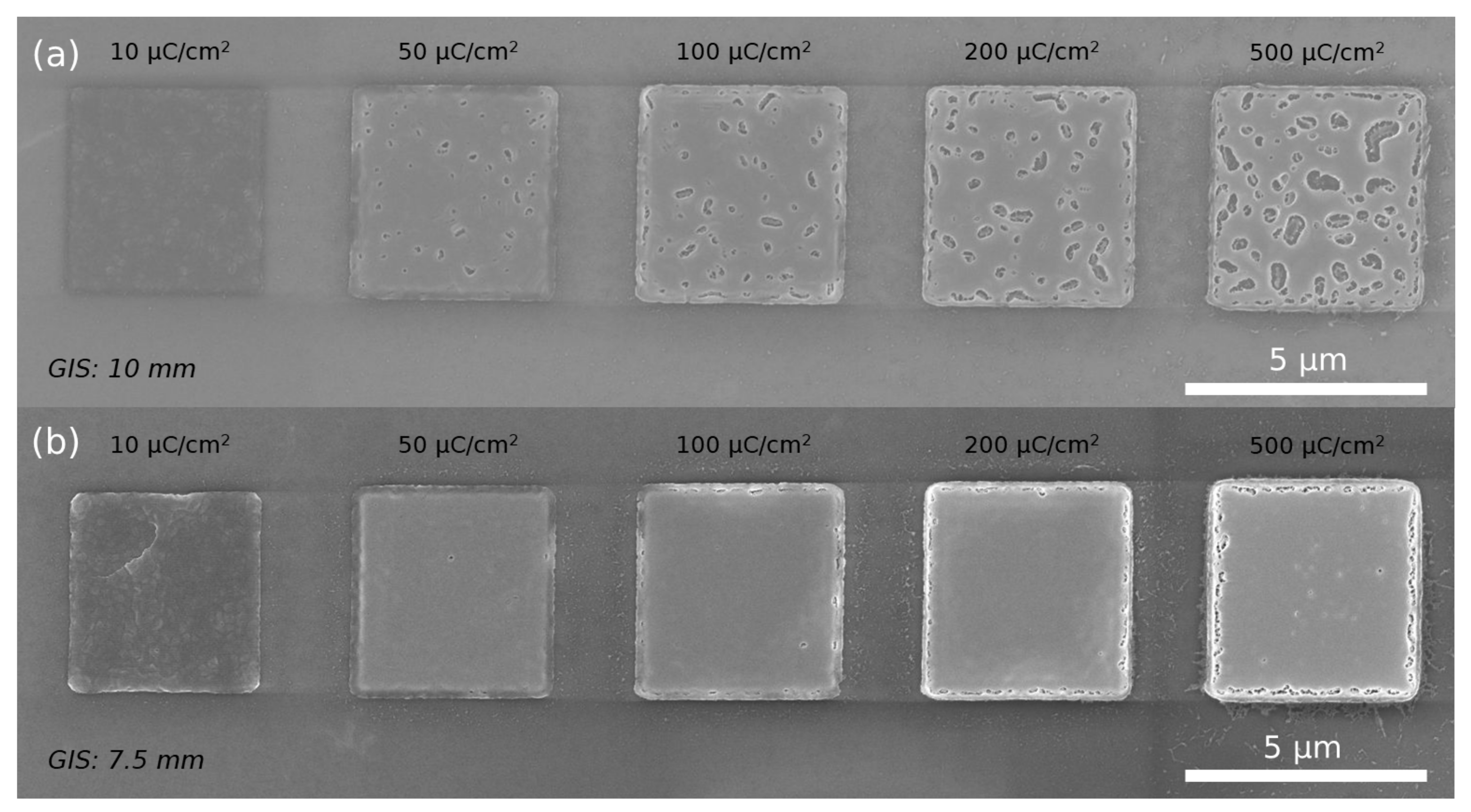
The effect of the dose was tested by growing four m W–C squares with a fixed ion beam current of 7.7 pA and varying the ion dose between 10 and 500 C/cm (Figure 2). All irradiation times are in the order of seconds, whereas growing one of these squares at room temperature (with an optimized volume per dose of 0.082 m/nC) would require an estimated dose of 61,000 m/nC, taking roughly 20 min.
The 2.5 mm difference in the GIS–sample distance has a profound and evident effect on the integrity of the samples—those grown further apart from the GIS appear to have more holes, with areas where the lack of precursor results in the appearance of cavities. This issue is overcome if the working distance is decreased to 7.5 mm, where the presumably enhanced availability of precursor condensate allows for the deposit to be fully grown. While 10 mm has been shown to be sufficient for Cryo-FIBID of W(CO) at −100 C, the 40 C difference appears to require a greater amount of precursor material.
For both GIS–sample distances, the lowest assessed value of ion dose yields a thin, non-homogeneous layer of material, while the upper end of the studied range results in the appearance of holes. Both effects can be attributed to the condensate layer’s under and over-exposure, thus indicating an optimal value for this parameter in the intermediate region in the 50–200 C/cm range. Again, these values are comparable, yet slightly above those retrieved in −100 C Cryo-FIBID of W(CO).
The metallic content of the deposits increases with the ion dose used to grow them, as revealed by EDX measurements performed in independent arrays of W–C squares nominally identical to those shown in Figure 2b (see the Supplementary Materials). Even though it is not possible to retrieve a precise figure of the amount of W using SEM-EDX only due to the reduced thickness of the deposits, the results are compatible with an atomic W content in the 20–30% range in deposits grown with ion doses of 50 C/cm and above.
3.2. Electrical Resistivity
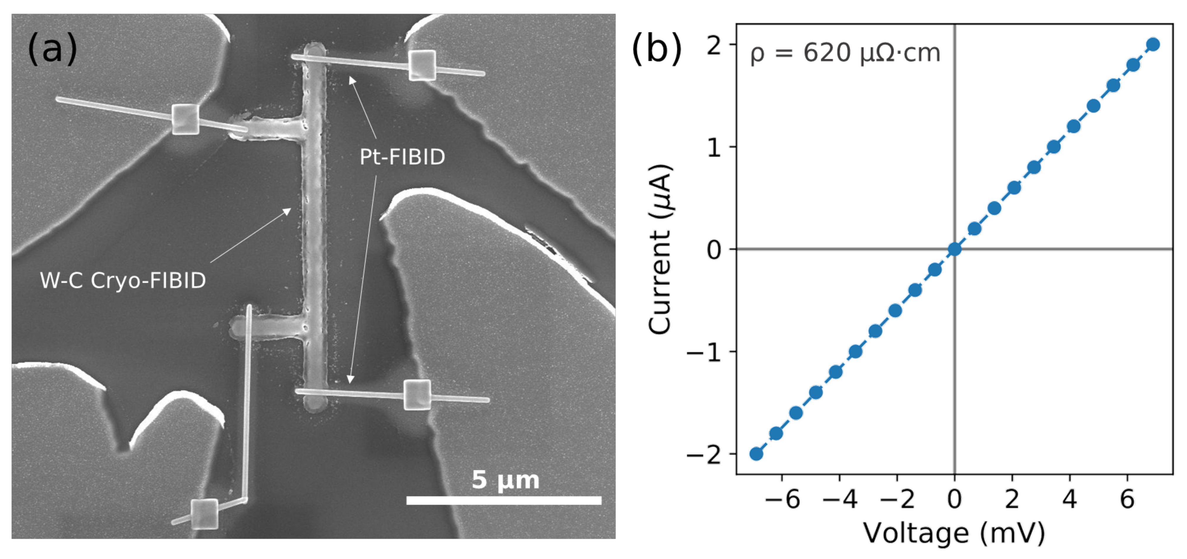
The resistivity of the material was investigated by performing electrical measurements in a 5 m-long, 400 nm-wide nanowire grown with an ion dose of 200 C/cm. Specifically, current–voltage characteristics were retrieved in the aforementioned microprobe station, using a four-probe configuration. The nanowires were joined to the lithographied Ti pads using intermediate Pt–C contacts grown in situ by Ga FIBID (Figure 3a). The Pt–C material is metallic [19] and is thus adequate for this purpose. Side effects arising from the FIBID procedure are limited to the regions very close to the two central contacts (a few hundreds of nanometers at most). The influence of these side effects to the overall electrical behavior of the measured sample along the 5 m-long current-carrying central path of the nanowire (between the two voltage leads) is thus small [20]. Pt-FIBID-induced ion implantation, amorphization, or halo deposition are therefore constrained to a small sample volume and do not significantly influence the electrical measurement.
The voltage drop across the nanostructure is linear with the current in the investigated range (Figure 3b) and corresponds to an ohmic resistance of k. FIB/SEM cross-sectioning revealed an elongated cross-sectional shape, with an average thickness of 20 nm and a cross-sectional area A of around 9000 nm. With a nanowire length of m, the associated resistivity is therefore estimated to be 620 cm.
4. Conclusions and Outlook
A parallel approach to the conventional, coolant-based Cryo-FIBID of W(CO) carried out at −100 C is presented: a thermoelectric plate can be utilized to perform Cryo-FIBID at −60 C, maintaining the quality and properties of the W–C deposits. The deposition at this temperature requires a slightly higher ion dose and a reduced GIS–sample distance (200 C/cm and 7.5 mm, compared to 55 C/cm and 10 mm, respectively), yet the processing speed is between two to three orders of magnitude above that of room-temperature FIBID. A resistivity around 620 cm is retrieved for the material deposited in these conditions, which is comparable to but lower than that obtained in −100 C Cryo-FIBID (800–900 cm).
The relatively unexplored nature of Cryo-FIBID makes this approach an equally appealing and unbeaten path, with an ample spectrum of experimental parameters to investigate and optimize, which are not only limited to the ion dose and GIS–sample distance presented here, but also include the ion beam current, dwell time, and precursor type. The lack of vibrations induced by a cooling agent can also be exploited to explore the resolution capabilities of this technique, which is expected to depend on the ion beam current and acceleration voltage.
From a broader point of view, −60 C Cryo-FIBID W–C (and in principle, other materials, provided a growth optimization process is developed for the corresponding precursor) represents an appealing merging of the flexibility and targeting capability of conventional FIBID with the processing speeds and lack of sample damage of larger-scale lithography approaches. As such, it can be utilized to fabricate electrical contacts on nanowires and 2D materials without damaging them, as well as to grow deposits in sizes out of the adequate range of conventional FIBID, with applications in circuit editing and mask repair. In addition, installing a thermoelectric plate is faster, simpler, safer, and more affordable than setting up a liquid nitrogen-based cooling system, which facilitates the implementation of this technique by the industry and research communities.
Overall, the possibility of approaching Cryo-FIBID without the hassle of a cooling agent flowing through the sample stage represents a highly promising step towards the fabrication of advanced devices using this technique, and a further reassurance of its latent potential.
Supplementary Materials
The following are available at https://www.mdpi.com/article/10.3390/app112110123/s1, Figure S1: Estimated dependence of the composition with the ion dose. Table S1: EDX quantification of the studied interaction volume.
Author Contributions
Investigation, Visualization, Writing—original draft preparation, P.O.; Conceptualization, Supervision, Project Administration, Funding acquisition, J.M.D.T.; Writing—review and editing, P.O., F.S., S.S. and J.M.D.T. All authors have read and agreed to the published version of the manuscript.
Funding
This research was funded by European Union’s Horizon 2020 research and innovation program with grant number 892427. This project was supported by the Spanish Ministry of Science through grant numbers MAT2017-82970-C2-1-R, MAT2017-82970-C2-2-R and PID2020-112914RB-100, including FEDER funding, from CSIC through project PIE202060E187, and by Gobierno de Aragón through the grant number E13_20R with European Social Fund (Construyendo Europa desde Aragón). The following networking projects are acknowledged: Spanish Nanolito (MAT2018-102627-T) and COST-FIT4NANO (action CA19140).
Acknowledgments
The microscopy works were conducted in the Laboratory for Advanced Microscopies (LMA), at the Institute of Nanoscience and Materials of Aragón (INMA)—University of Zaragoza. Authors acknowledge the LMA for offering access to their instruments and expertise. The experimental support of L. Casado in the instrument set-up and electrical characterization is acknowledged. P. Orús acknowledges fruitful discussions on the matter held with A. Salvador.
Conflicts of Interest
The authors declare no conflict of interest.
References
- Utke, I.; Hoffmann, P.; Melngailis, J. Gas-assisted focused electron beam and ion beam processing and fabrication. J. Vac. Sci. Technol. B Microelectron. Nanometer Struct. Process. Meas. Phenom. 2008, 26, 1197–1276. [Google Scholar] [CrossRef] [Green Version]
- Orús, P.; Córdoba, R.; De Teresa, J.M. Focused Ion Beam Induced Processing. In Nanofabrication: Nanolithography Techniques and Their Applications; De Teresa, J., Ed.; IOP Publishing: Bristol, UK, 2020. [Google Scholar] [CrossRef]
- Sadki, E.; Ooi, S.; Hirata, K. Focused-ion-beam-induced deposition of superconducting nanowires. Appl. Phys. Lett. 2004, 85, 6206–6208. [Google Scholar] [CrossRef] [Green Version]
- Gannon, T.J.; Gu, G.; Casey, J.D.; Huynh, C.; Bassom, N.; Antoniou, N. Focused ion beam induced deposition of low-resistivity copper material. J. Vac. Sci. Technol. B Microelectron. Nanometer Struct. Process. Meas. Phenom. 2004, 22, 3000–3003. [Google Scholar] [CrossRef]
- Tao, T.; Ro, J.; Melngailis, J.; Xue, Z.; Kaesz, H.D. Focused ion beam induced deposition of platinum. J. Vac. Sci. Technol. B Microelectron. Process. Phenom. 1990, 8, 1826–1829. [Google Scholar] [CrossRef]
- Shedd, G.; Lezec, H.; Dubner, A.; Melngailis, J. Focused ion beam induced deposition of gold. Appl. Phys. Lett. 1986, 49, 1584–1586. [Google Scholar] [CrossRef]
- Sanz-Martín, C.; Magén, C.; De Teresa, J.M. High volume-per-dose and low resistivity of cobalt nanowires grown by Ga+ focused ion beam induced deposition. Nanomaterials 2019, 9, 1715. [Google Scholar] [CrossRef] [PubMed] [Green Version]
- Hutcheson, G.D. Moore’s law, lithography, and how optics drive the semiconductor industry. In Extreme Ultraviolet (EUV) Lithography IX; International Society for Optics and Photonics: Bellingham, WA, USA, 2018; Volume 10583, p. 1058303. [Google Scholar]
- Grigorescu, A.; Hagen, C. Resists for sub-20-nm electron beam lithography with a focus on HSQ: State of the art. Nanotechnology 2009, 20, 292001. [Google Scholar] [CrossRef] [PubMed] [Green Version]
- Córdoba, R.; Orús, P.; Strohauer, S.; Torres, T.E.; De Teresa, J.M. Ultra-fast direct growth of metallic micro-and nano-structures by focused ion beam irradiation. Sci. Rep. 2019, 9, 14076. [Google Scholar] [CrossRef] [PubMed] [Green Version]
- De Teresa, J.M.; Orús, P.; Córdoba, R.; Philipp, P. Comparison between focused electron/ion beam-induced deposition at room temperature and under cryogenic conditions. Micromachines 2019, 10, 799. [Google Scholar] [CrossRef] [PubMed] [Green Version]
- Bresin, M.; Thiel, B.; Toth, M.; Dunn, K. Focused electron beam-induced deposition at cryogenic temperatures. J. Mater. Res. 2011, 26, 357–364. [Google Scholar] [CrossRef]
- Bresin, M.; Toth, M.; Dunn, K. Direct-write 3D nanolithography at cryogenic temperatures. Nanotechnology 2012, 24, 035301. [Google Scholar] [CrossRef] [PubMed]
- Berger, L.; Jurczyk, J.; Madajska, K.; Szymańska, I.B.; Hoffmann, P.; Utke, I. Room Temperature Direct Electron Beam Lithography in a Condensed Copper Carboxylate. Micromachines 2021, 12, 580. [Google Scholar] [CrossRef] [PubMed]
- Salvador-Porroche, A.; Sangiao, S.; Philipp, P.; Cea, P.; De Teresa, J.M. Optimization of Pt-C deposits by Cryo-FIBID: Substantial growth rate increase and quasi-metallic behaviour. Nanomaterials 2020, 10, 1906. [Google Scholar] [CrossRef] [PubMed]
- Salvador-Porroche, A.; Sangiao, S.; Magen, C.; Barrado, M.; Philipp, P.; Belotcerkovtceva, D.; Mutta, V.K.; Cea, P.; De Teresa, J.M. Highly-efficient growth of cobalt nanostructures using focused ion beam induced deposition under cryogenic conditions: Application to electrical contacts on graphene, magnetism and hard masking. Nanoscale Adv. 2021, 3, 5656–5662. [Google Scholar] [CrossRef]
- Schilling, A.; Adams, T.; Bowman, R.; Gregg, J. Strategies for gallium removal after focused ion beam patterning of ferroelectric oxide nanostructures. Nanotechnology 2007, 18, 035301. [Google Scholar] [CrossRef] [PubMed]
- Drezner, Y.; Fishman, D.; Greenzweig, Y.; Raveh, A. Characterization of damage induced by FIB etch and tungsten deposition in high aspect ratio vias. J. Vac. Sci. Technol. B Nanotechnol. Microelectron. Mater. Process. Meas. Phenom. 2011, 29, 011026. [Google Scholar] [CrossRef]
- Fernández-Pacheco, A.; De Teresa, J.; Córdoba, R.; Ibarra, M. Metal-insulator transition in Pt-C nanowires grown by focused-ion-beam-induced deposition. Phys. Rev. B 2009, 79, 174204. [Google Scholar] [CrossRef]
- Hiley, C.; Scanlon, D.; Sokol, A.; Woodley, S.; Ganose, A.; Sangiao, S.; De Teresa, J.; Manuel, P.; Khalyavin, D.; Walker, M.; et al. Antiferromagnetism at T > 500 K in the layered hexagonal ruthenate SrRu2O6. Phys. Rev. B 2015, 92, 104413. [Google Scholar] [CrossRef] [Green Version]
Figure 1.
Open chamber of the Helios 650 NanoLab FIB/SEM microscope with the MHCS mounted.

Figure 2.
W–C squares deposited with variable ion doses at a distance from the GIS of (a) 10 mm, and (b) 7.5 mm. The deposition times are, for each square, and in order of increasing dose, 0.2, 1.0, 2.1, 4.2, and 10.3 s.
Figure 2.
W–C squares deposited with variable ion doses at a distance from the GIS of (a) 10 mm, and (b) 7.5 mm. The deposition times are, for each square, and in order of increasing dose, 0.2, 1.0, 2.1, 4.2, and 10.3 s.

Figure 3.
(a) SEM image of a W–C Cryo-FIBID nanowire grown using an ion dose of 200 C/cm, joined to Ti pads by Pt-FIBID contacts. (b) Current–voltage characteristics of the nanowire. The dashed line indicates a linear fit that yields a resistance of 3.44 k.
Figure 3.
(a) SEM image of a W–C Cryo-FIBID nanowire grown using an ion dose of 200 C/cm, joined to Ti pads by Pt-FIBID contacts. (b) Current–voltage characteristics of the nanowire. The dashed line indicates a linear fit that yields a resistance of 3.44 k.

Publisher’s Note: MDPI stays neutral with regard to jurisdictional claims in published maps and institutional affiliations. |
© 2021 by the authors. Licensee MDPI, Basel, Switzerland. This article is an open access article distributed under the terms and conditions of the Creative Commons Attribution (CC BY) license (https://creativecommons.org/licenses/by/4.0/).
Share and Cite
MDPI and ACS Style
Orús, P.; Sigloch, F.; Sangiao, S.; De Teresa, J.M. Cryo-Focused Ion Beam-Induced Deposition of Tungsten–Carbon Nanostructures Using a Thermoelectric Plate. Appl. Sci. 2021, 11, 10123. https://doi.org/10.3390/app112110123
AMA Style
Orús P, Sigloch F, Sangiao S, De Teresa JM. Cryo-Focused Ion Beam-Induced Deposition of Tungsten–Carbon Nanostructures Using a Thermoelectric Plate. Applied Sciences. 2021; 11(21):10123. https://doi.org/10.3390/app112110123
Chicago/Turabian StyleOrús, Pablo, Fabian Sigloch, Soraya Sangiao, and José María De Teresa. 2021. "Cryo-Focused Ion Beam-Induced Deposition of Tungsten–Carbon Nanostructures Using a Thermoelectric Plate" Applied Sciences 11, no. 21: 10123. https://doi.org/10.3390/app112110123
Note that from the first issue of 2016, this journal uses article numbers instead of page numbers. See further details here.