


Low-Noise, Low-Power Readout IC for Two-Electrode ECG Recording Using Common-Mode Charge Pump for Robust 20-VPP Common-Mode Interference

Abstract
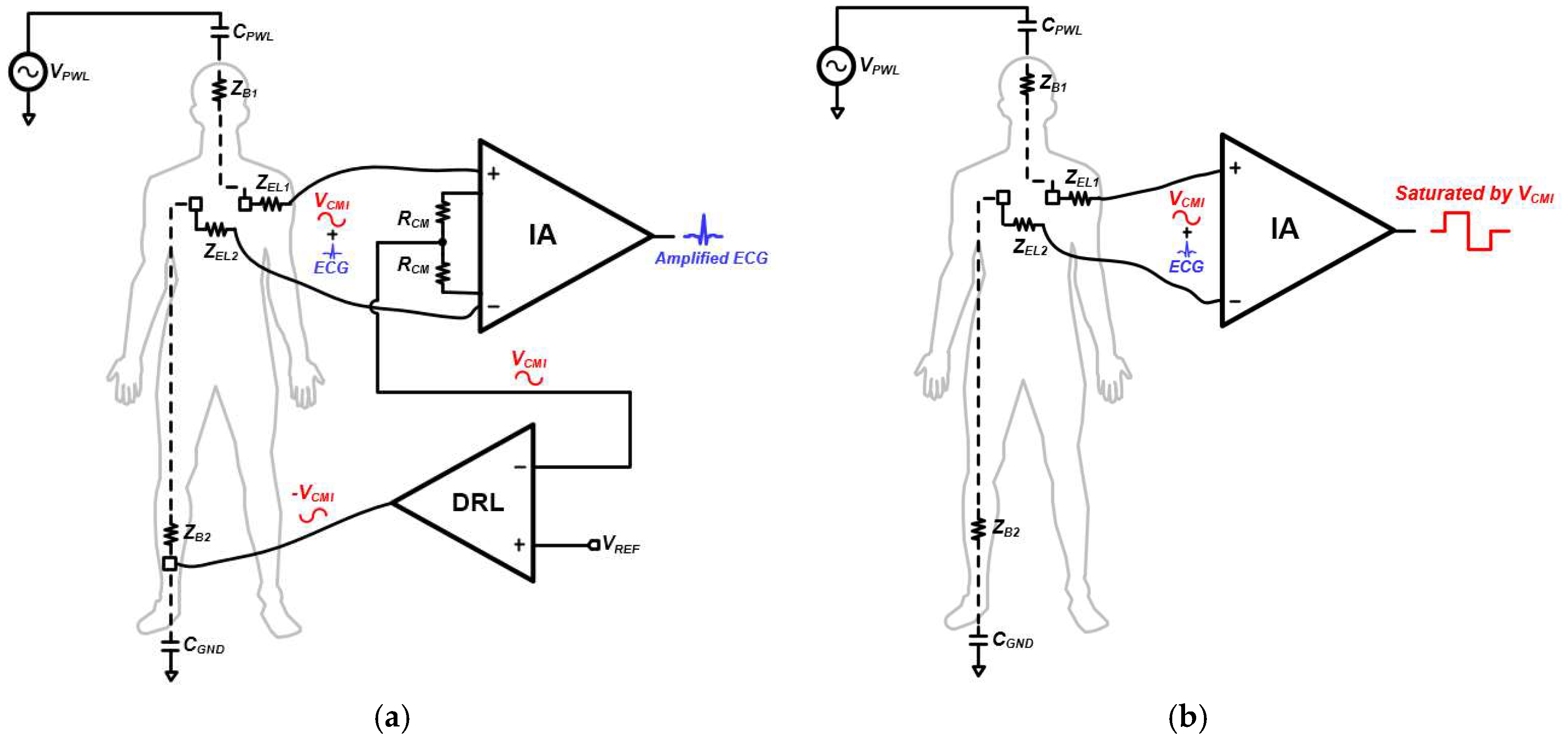
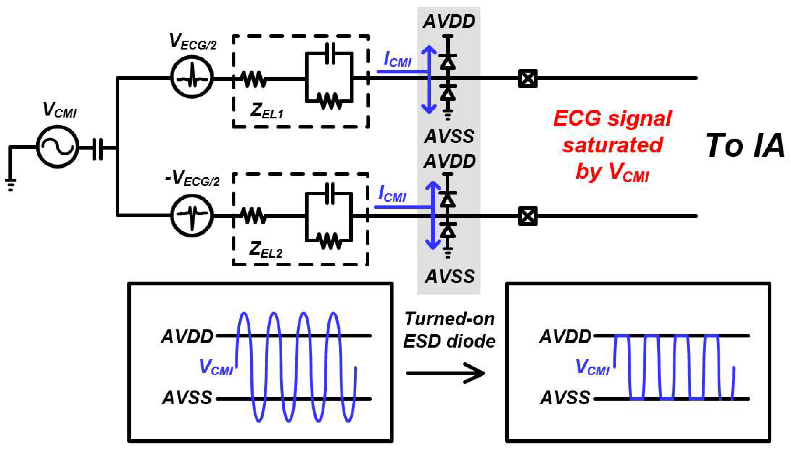
:1. Introduction
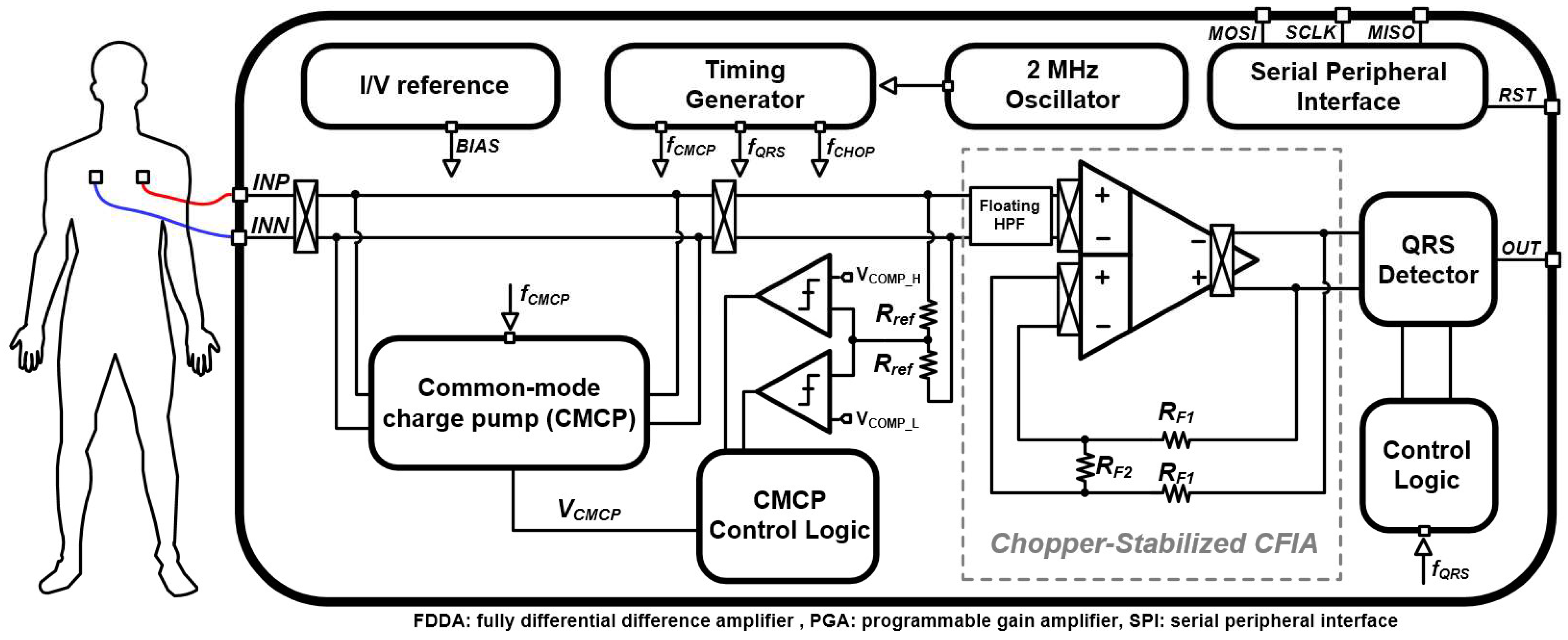
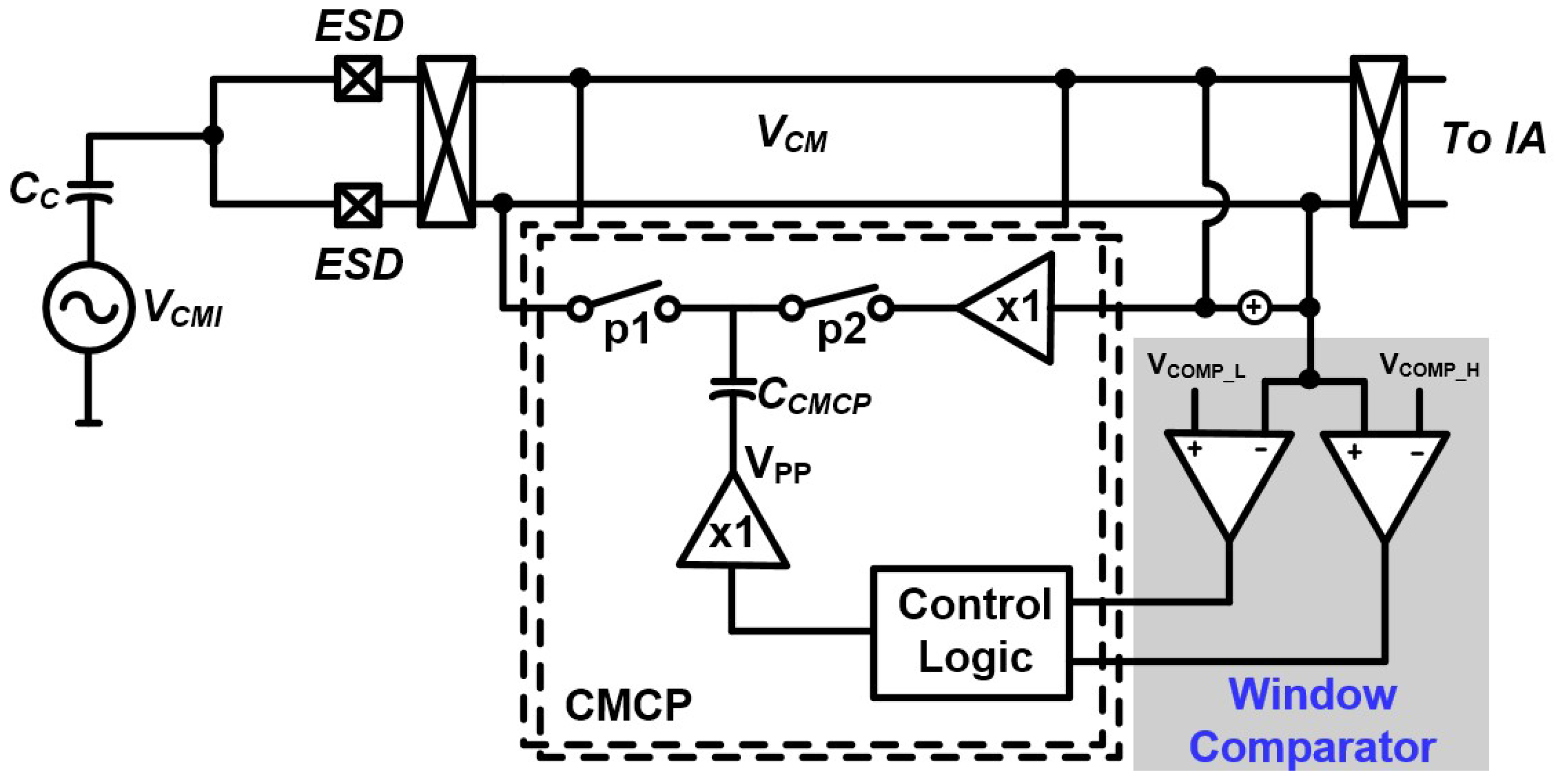
2. Circuit Implementation
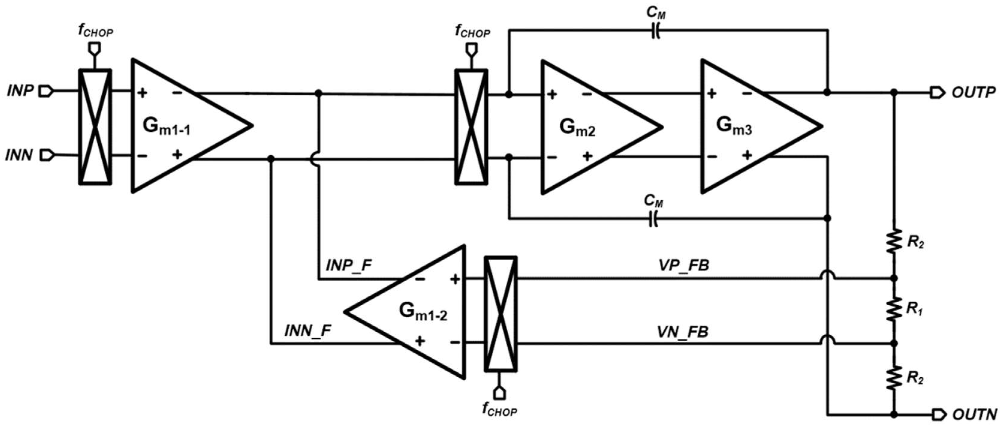
2.1. Top Architecture
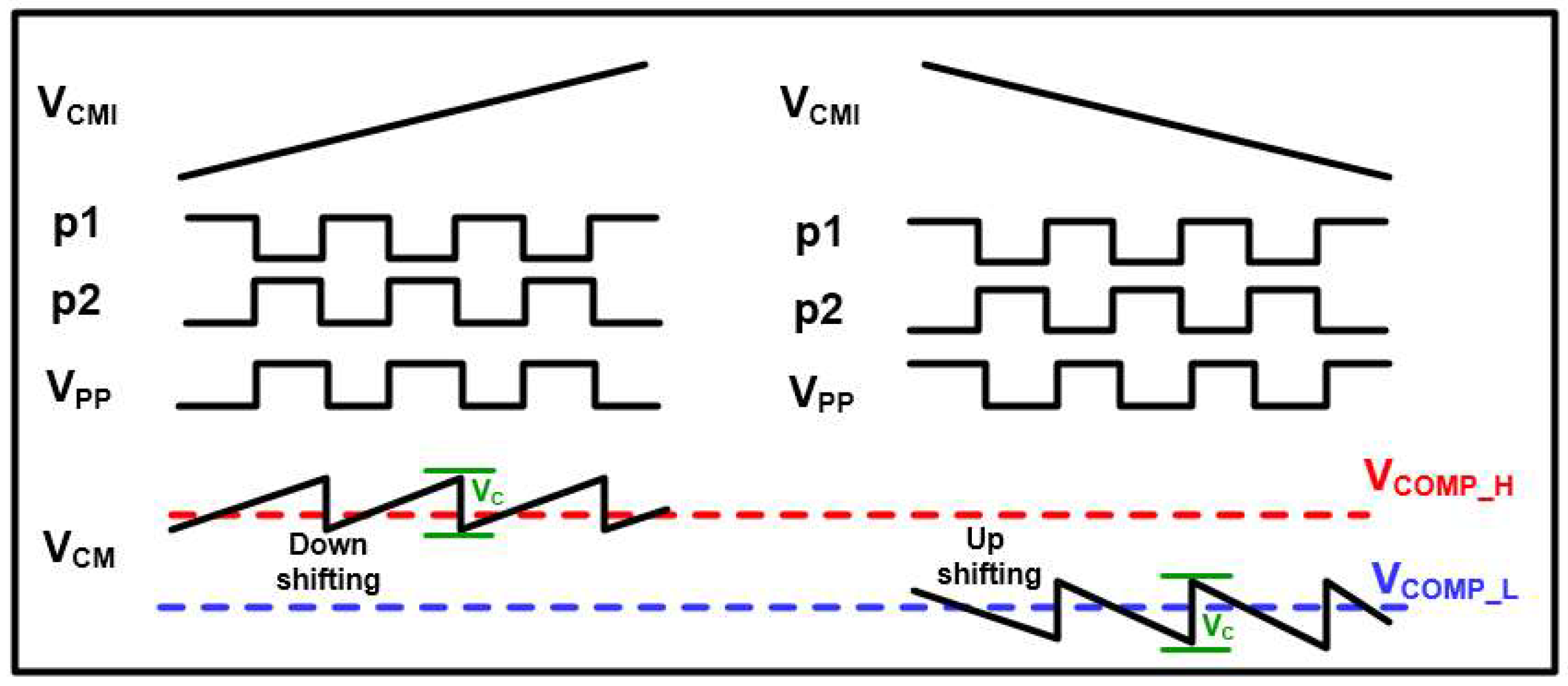
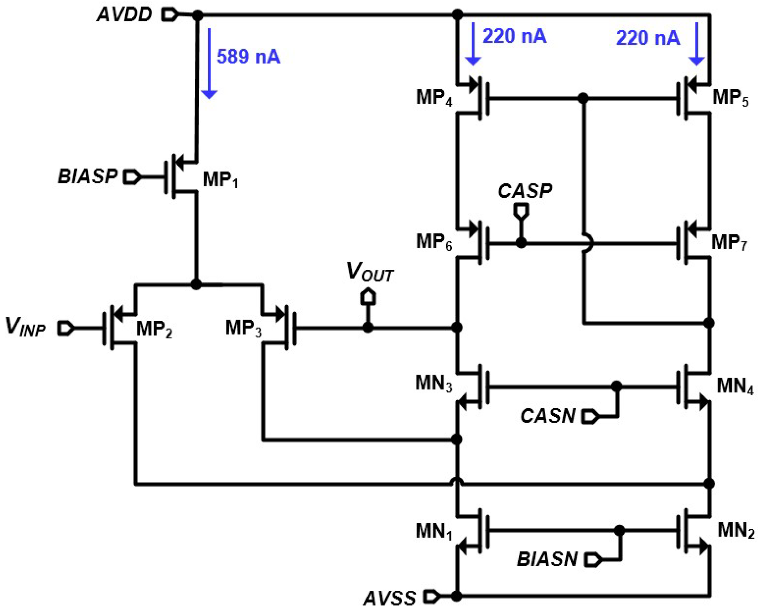
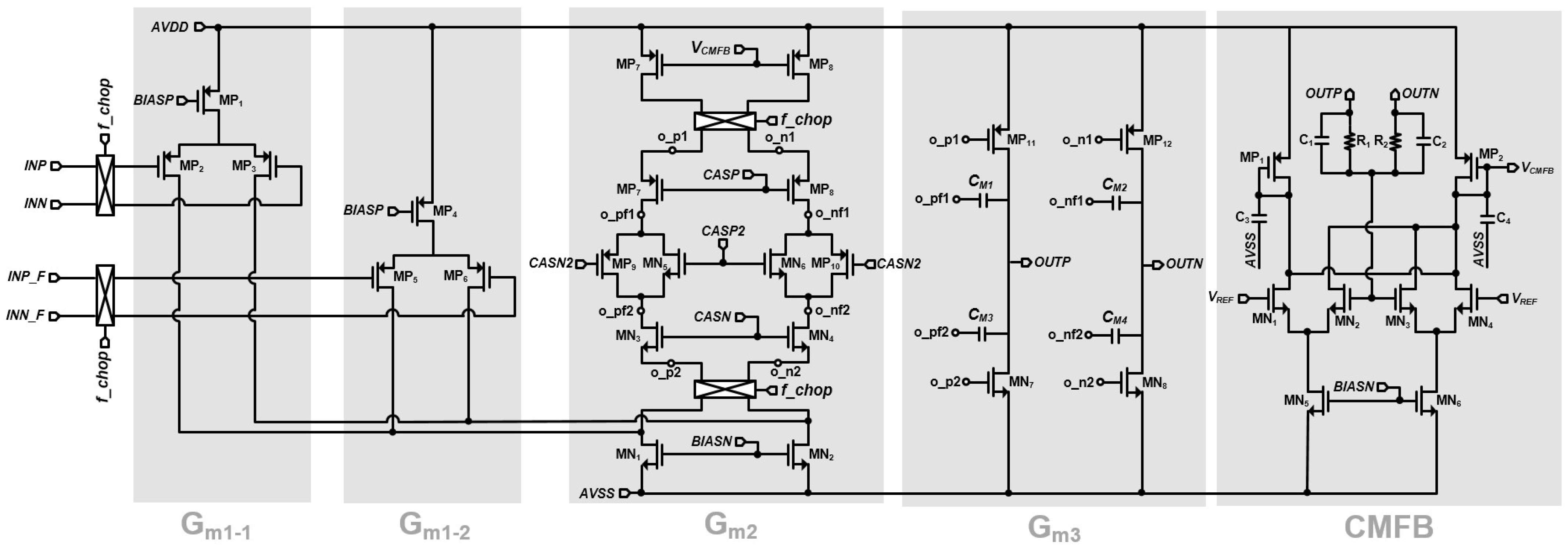
2.2. Common-Mode Charge Pump Stage
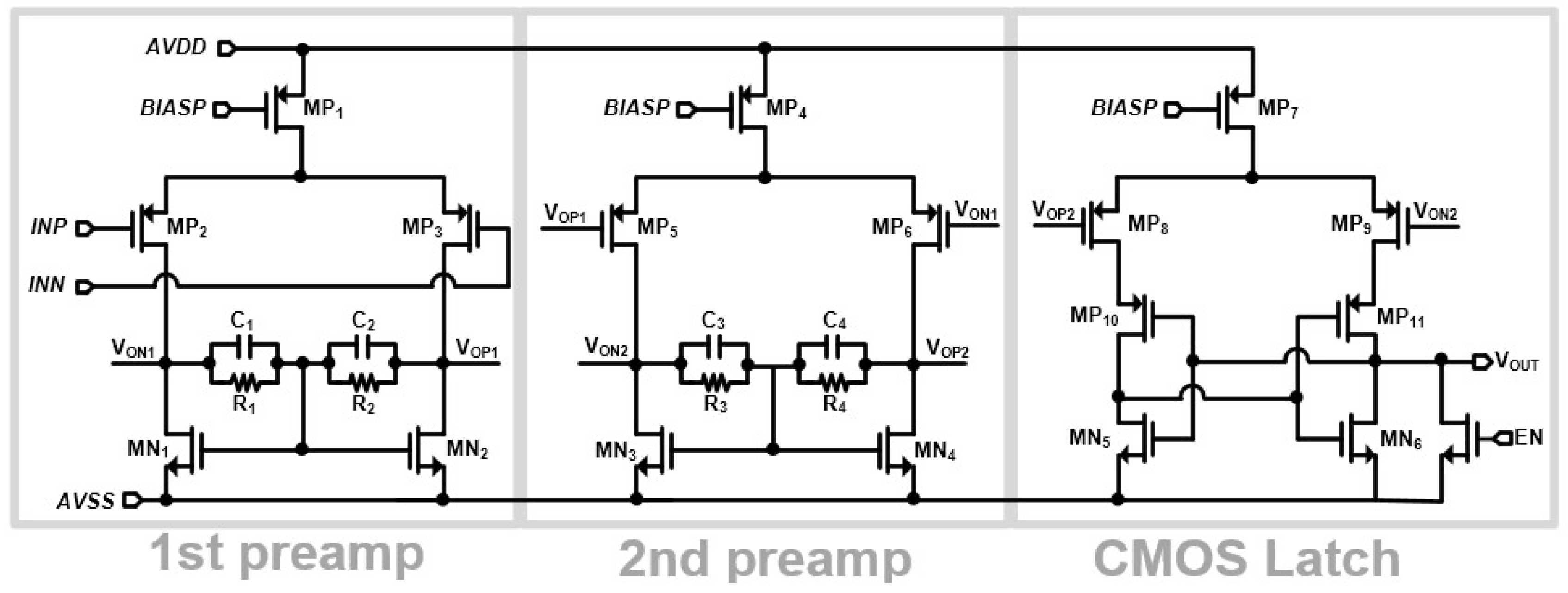
2.3. Amplifying Stage
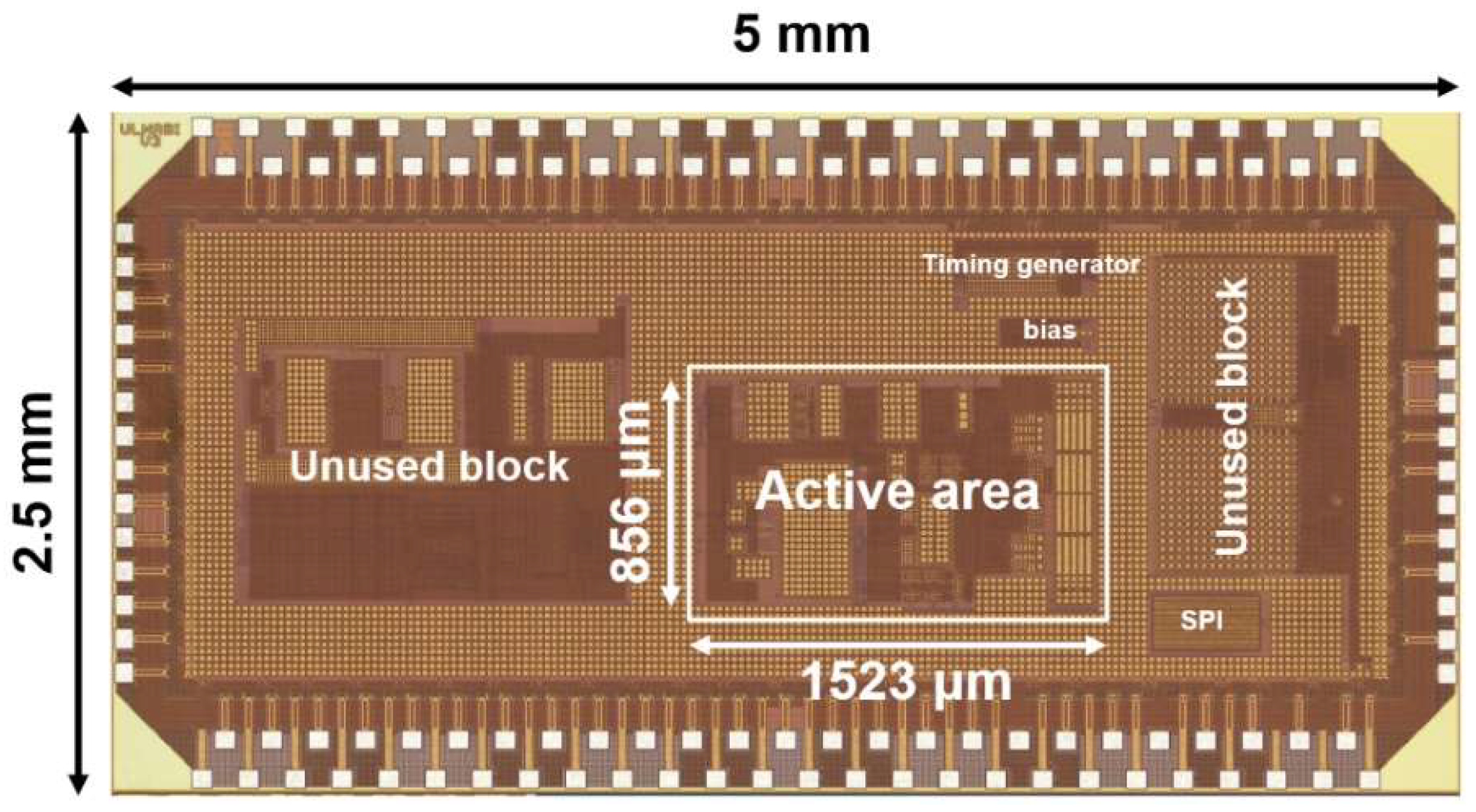
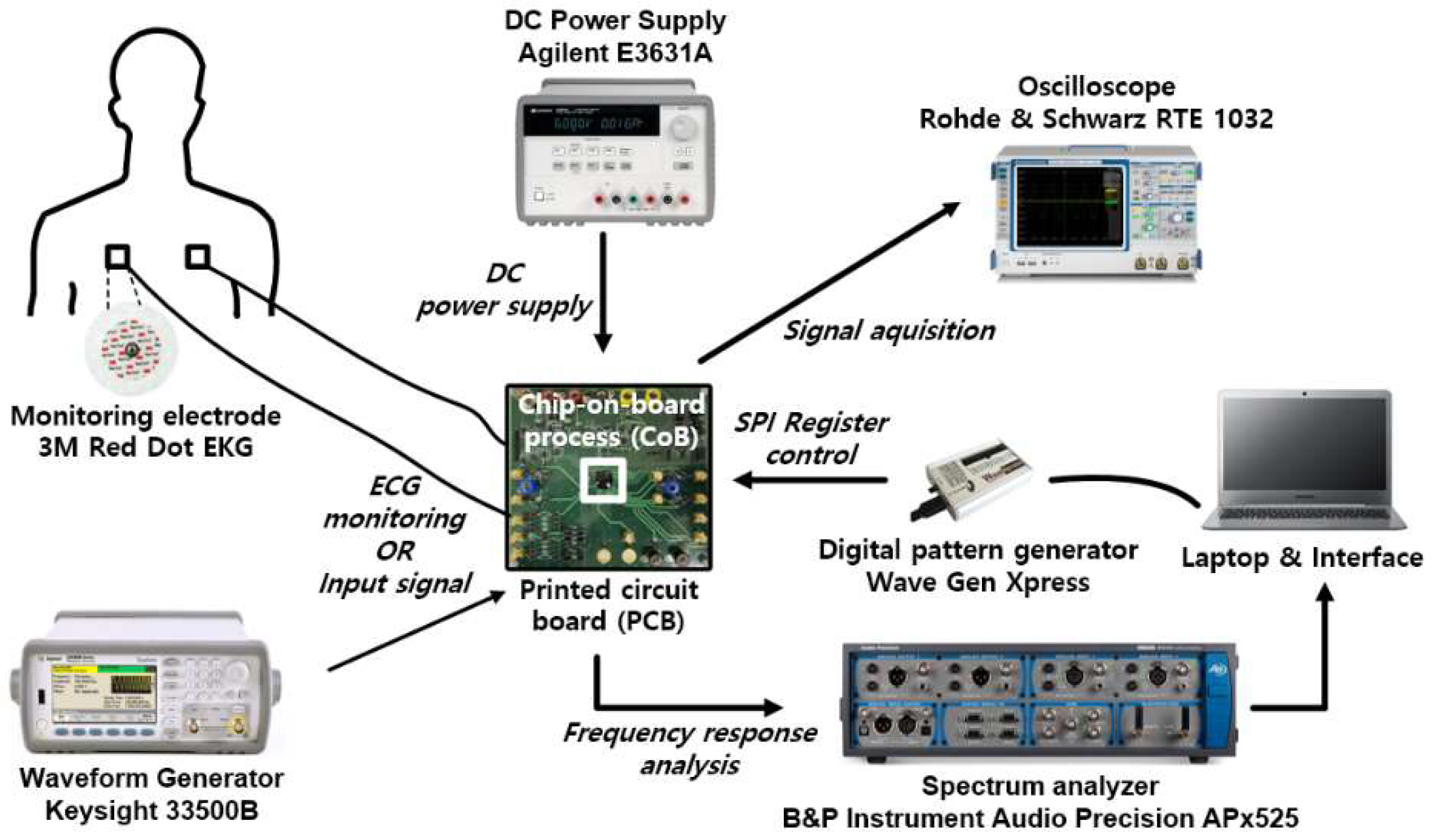
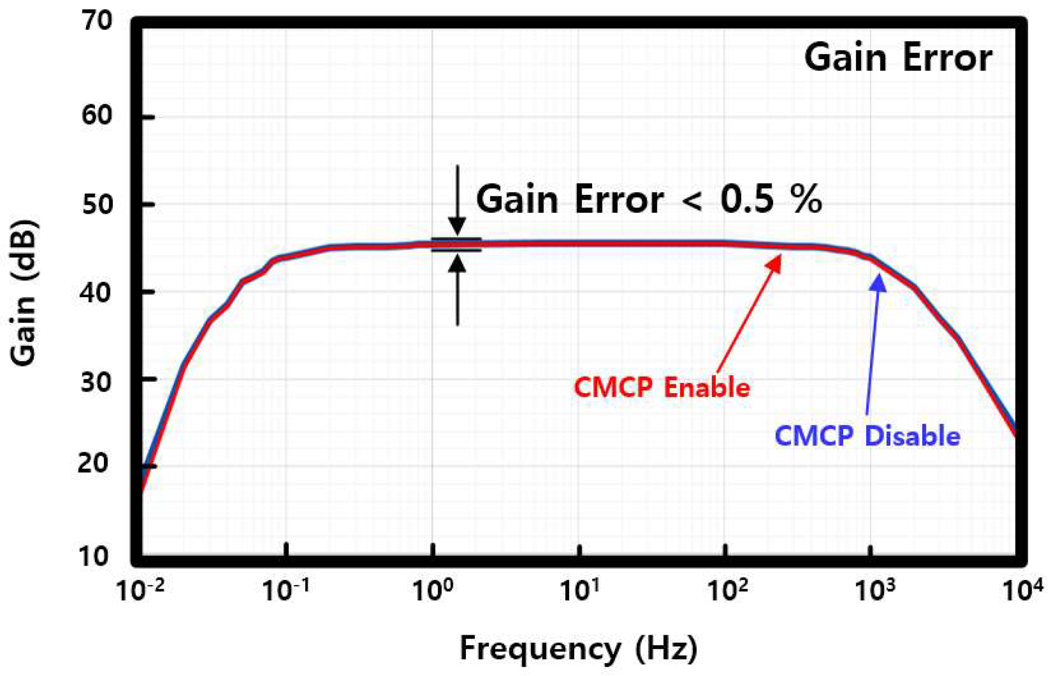
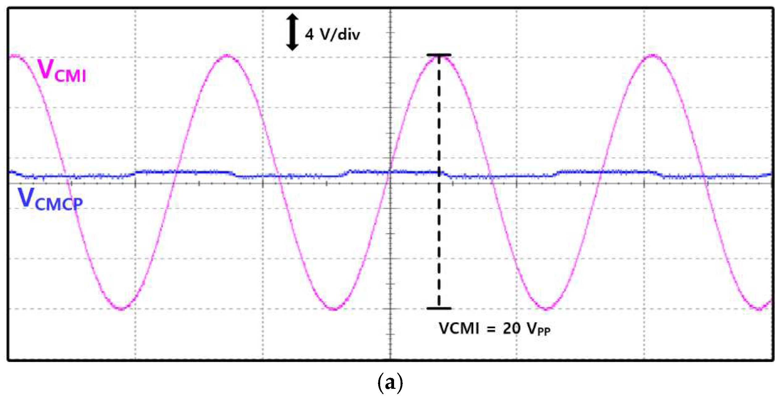
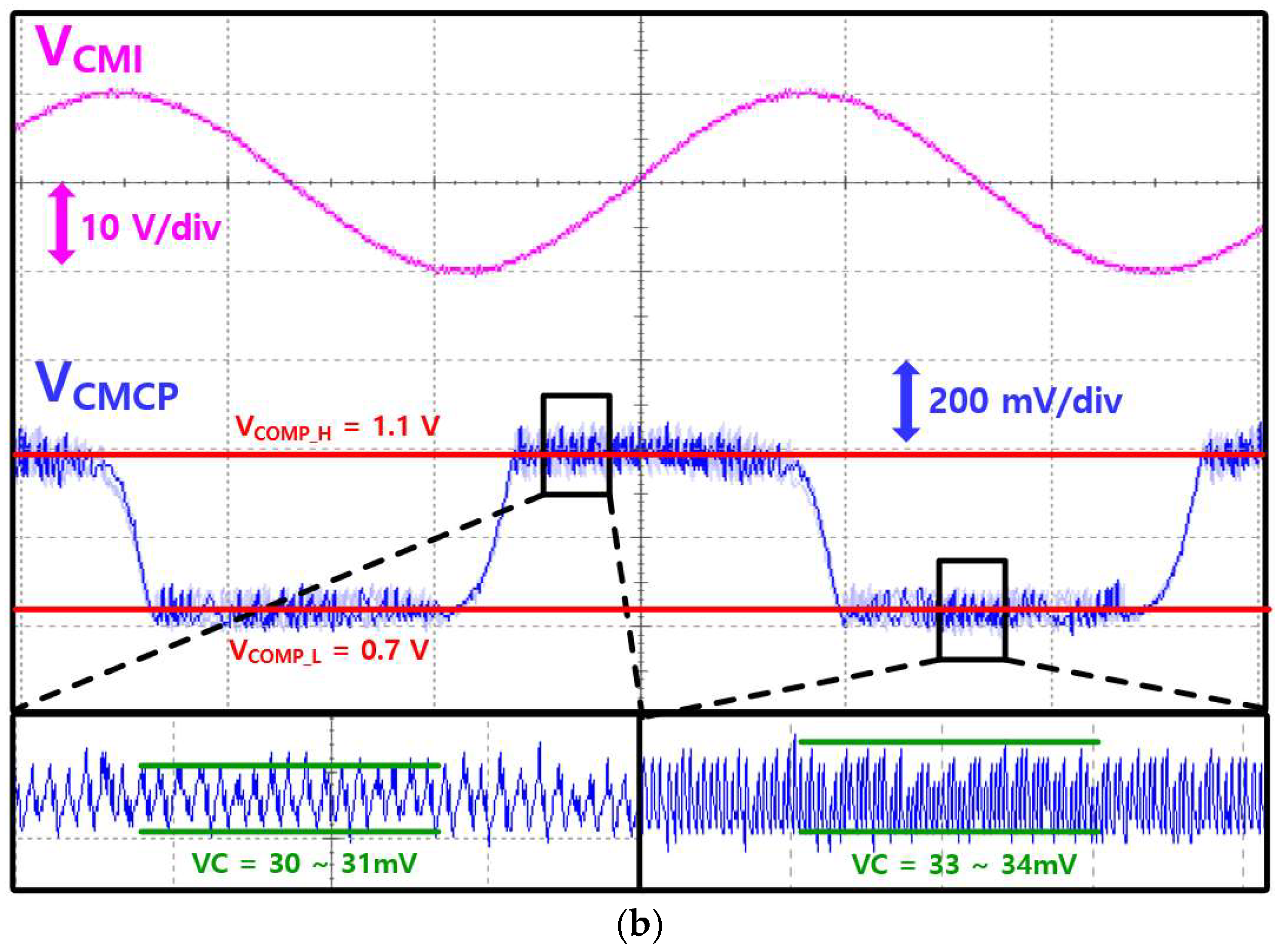
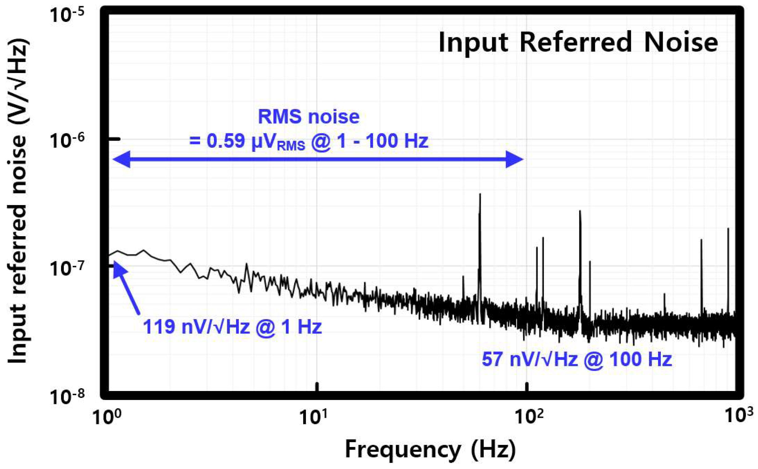
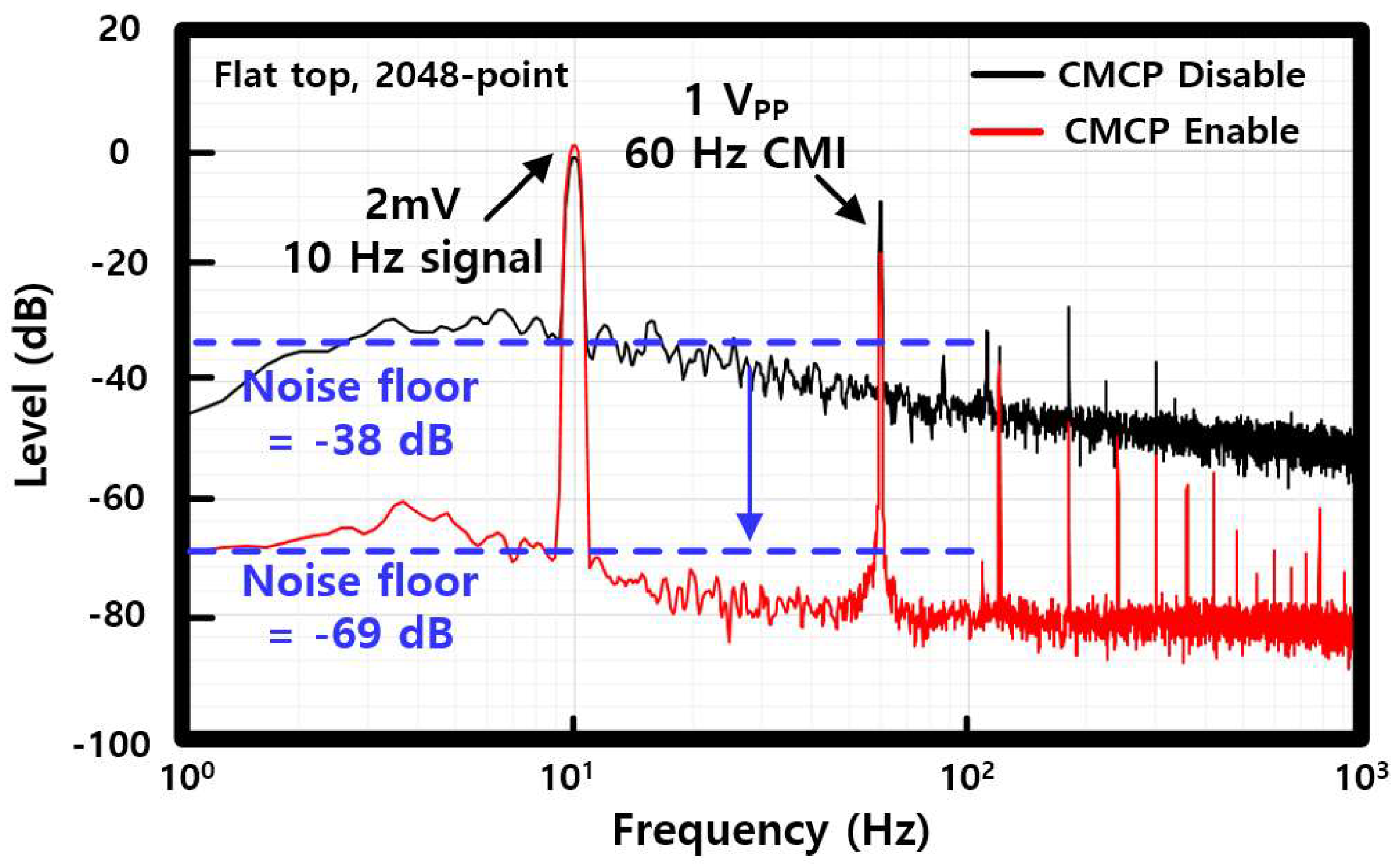
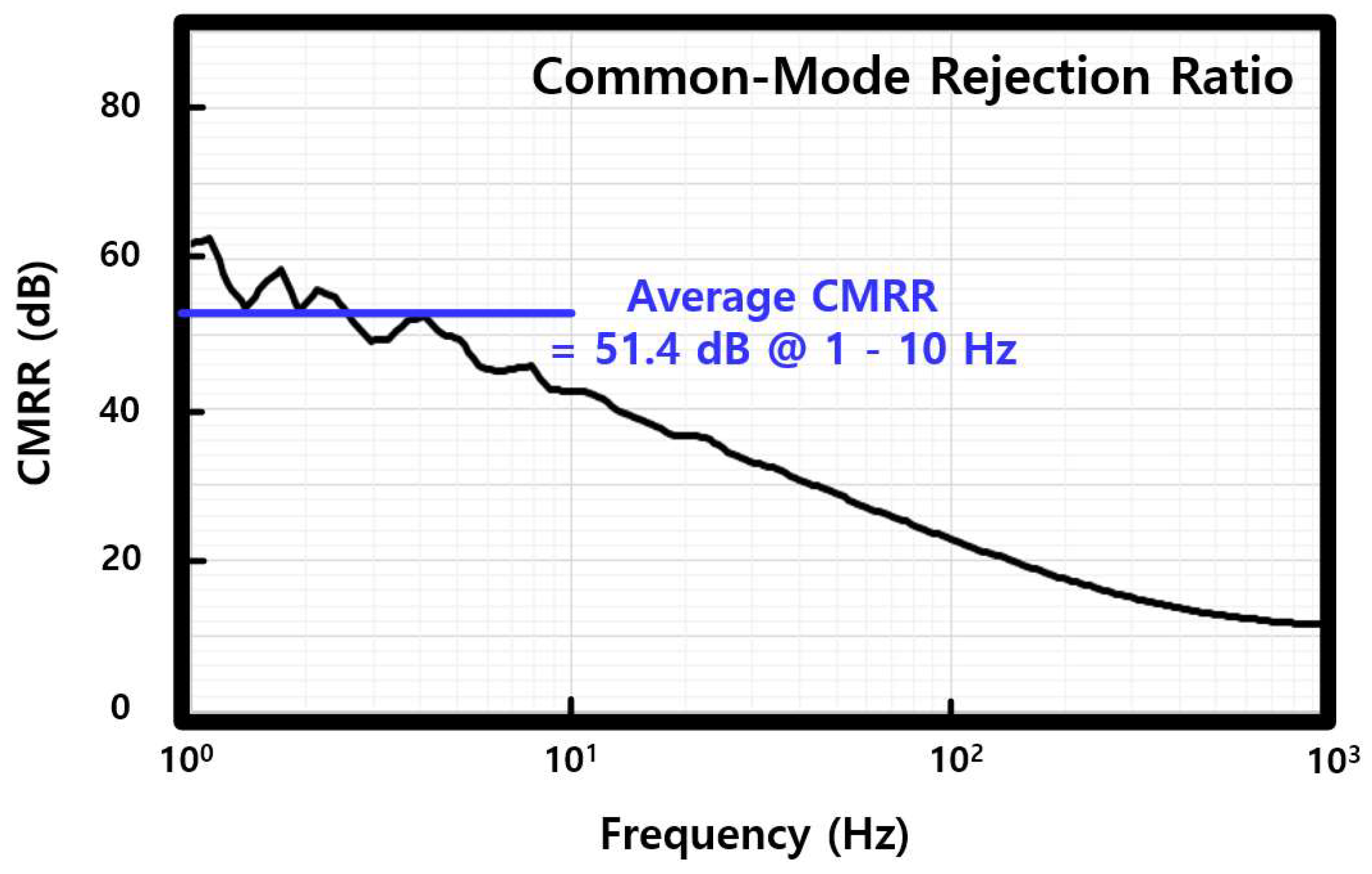
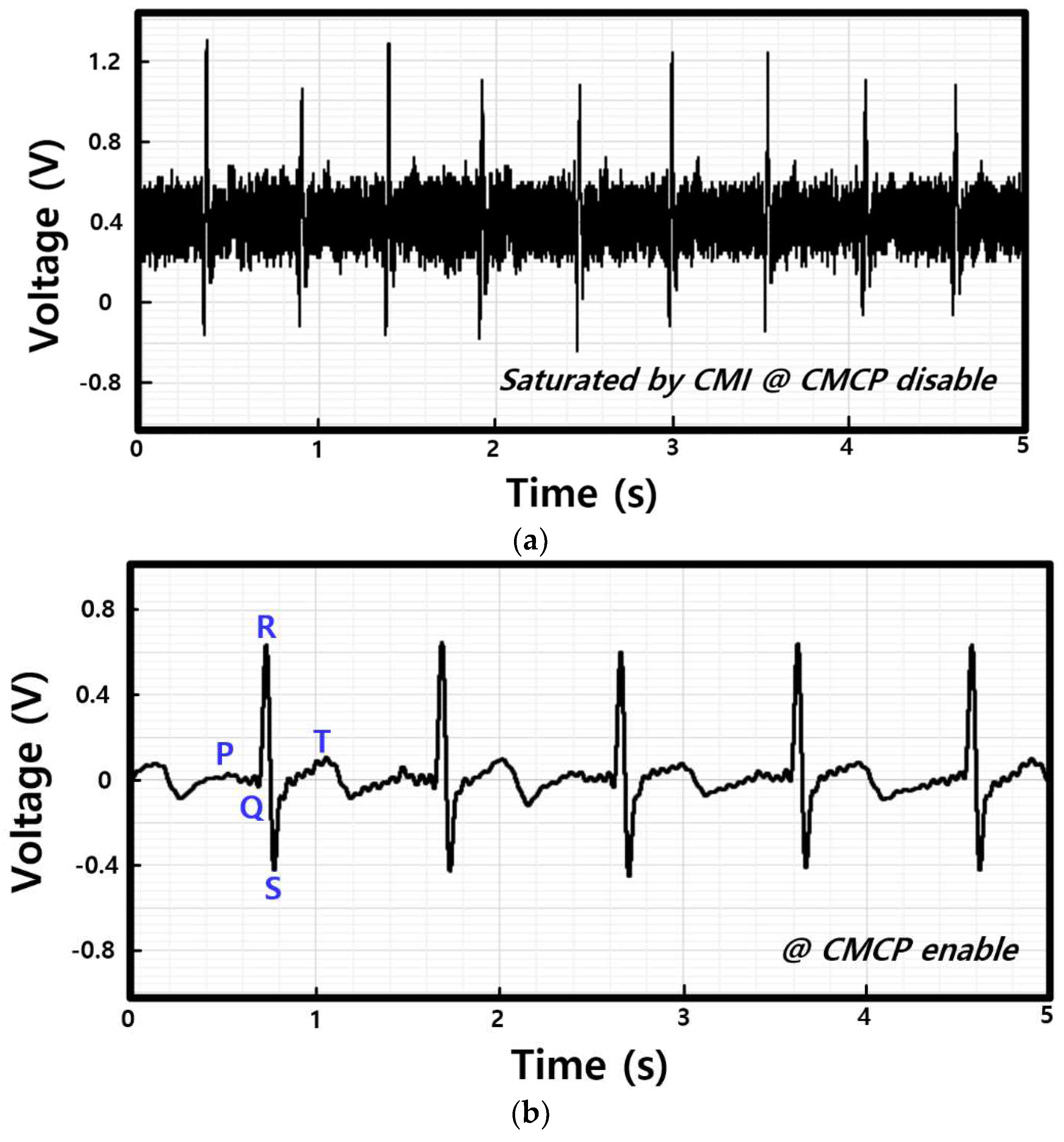
3. Measurement Results
4. Conclusions
Author Contributions
Funding
Institutional Review Board Statement
Informed Consent Statement
Data Availability Statement
Acknowledgments
Conflicts of Interest
References
- Bacquer, D.D.; Backer, G.D.; Kornitzer, M.; Blackburn, H. Prognostic Value of ECG findings for total, cardiovascular disease, and Coronary Heart Disease Death in men and Women. Heart 1998, 80, 570–577. [Google Scholar] [CrossRef] [PubMed] [Green Version]
- Sharma, M.; Rajendra, A. A New Method to Identify Coronary Artery Disease with ECG signals and Time-Frequency Concentrated Antisymmetric Biorthogonal Wavelet Filter Bank. Patten Recognit. Lett. 2019, 125, 235–240. [Google Scholar] [CrossRef]
- Bansal, A.; Joshi, R. Portable Out-of-Hospital Electrocardiography: A Review of Current Technologies. J. Arrhythmia 2018, 34, 129–138. [Google Scholar] [CrossRef] [PubMed]
- Koo, N.; Cho, S. A 24.88-μW Biopotential Amplifier Tolerant to 15-VPP Common-Mode Interference for Two-Electrode ECG Recording in 180-nm CMOS. IEEE J. Solid-State Circuits 2021, 56, 591–600. [Google Scholar] [CrossRef]
- Koo, N.; Cho, S. A 27.8 μW Biopotential Amplifier Tolerant to 30 VPP Common-Mode Interference for Two-electrode ECG Recording in 0.18 μm CMOS. In Proceedings of the IEEE International Solid-State Circuits Conference (ISSCC), San Francisco, CA, USA, 17–21 February 2019; pp. 366–367. [Google Scholar] [CrossRef]
- Thakor, N.V.; Webster, J.G. Ground-Free ECG Recording with Two Electrodes. IEEE Trans. Biomed. Eng. 1980, BME-27, 699–704. [Google Scholar] [CrossRef]
- Jedari, E.; Rashidzadeh, R.; Mirhassani, M.; Ahmadi, M. Two-Electrode ECG Measurement Circuit Using a Feed Forward CMRR Enhancement Method. In Proceedings of the IEEE 30th Canadian Conference on Electrical and Computer Engineering (CCECE), Windsor, ON, Canada, 30 April–3 May 2017. [Google Scholar] [CrossRef]
- You, D.; Heo, H.; Kim, H.; Kwon, Y.; Lee, S.; Ko, H. Power Line Interference Reduction Technique with a Current-Reused Current-Feedback Instrumentation Amplifier for ECG Recording. Appl. Sci. 2020, 10, 8478. [Google Scholar] [CrossRef]
- Winter, B.B.; Webster, J.G. Reduction of Interference Due to Common Mode Voltage in Biopotential Amplifiers. IEEE Trans. Biomed. Eng. 1983, BME-30, 58–62. [Google Scholar] [CrossRef]
- Sun, X. Low Noise, High Accuracy Analog Electrocardiogram (ECG) Signal Front End Amplifier for Wearable Equipment. In Proceedings of the 2021 International Conference on Electronics, Circuits and Information Engineering (ECIE), Zhengzhou, China, 22–24 January 2021; pp. 85–88. [Google Scholar] [CrossRef]
- Chen, L.; He, J.; Ge, F. A Low Power Low Noise ECG Amplifier Design Based on OTA. In Proceedings of the 2021 3rd International Conference on Intelligent Control, Measurement and Signal Processing and Intelligent Oil Field (ICMSP), Xi’an, China, 23–25 July 2021; pp. 230–233. [Google Scholar] [CrossRef]
- Chu, H.; Yan, Y.; Gan, L.; Jia, H.; Qian, L.; Huan, Y.; Zheng, L.; Zou, Z. A Neuromorphic Processing System with Spike-Driven SNN Processor for Wearable ECG Classification. IEEE Trans. Biomed. Circuits Syst. 2022, 16, 511–523. [Google Scholar] [CrossRef]
- Sharifshazileh, M.; Burelo, K.; Sarnthein, J.; Indiveri, G. An Electronic Neuromorphic System for Real-Time Detection of High Frequency Oscillations (HFO) in Intracranial EEG. Nat. Commun. 2021, 12, 3095. [Google Scholar] [CrossRef]
- Ribeiro, A.H.; Ribeiro, M.H.; Paixão, G.M.; Oliveira, D.M.; Gomes, P.R.; Canazart, J.A.; Ferreira, M.P.; Andersson, C.R.; Macfarlane, P.W.; Meira, W., Jr.; et al. Automatic diagnosis of the 12-lead ECG using a deep neural network. Nat. Commun. 2020, 11, 1760. [Google Scholar] [CrossRef] [Green Version]
- Yang, S.; Deng, B.; Wang, J.; Li, H.; Lu, M.; Che, Y.; Wei, X.; Loparo, K.A. Scalable Digital Neuromorphic Architecture for Large-Scale Biophysically Meaningful Neural Network with Multi-Compartment Neurons. IEEE Trans. Neural Netw. Learn. Syst. 2020, 31, 148–162. [Google Scholar] [CrossRef] [PubMed]
- Yang, S.; Wang, J.; Deng, B.; Azghadi, M.R.; Linares-Barranco, B. Neuromorphic Context-Dependent Learning Framework with Fault-Tolerant Spike Routing. IEEE Trans. Neural Netw. Learn. Syst. 2021, 33, 7126–7140. [Google Scholar] [CrossRef]
- Yang, S.; Wang, J.; Hao, X.; Li, H.; Wei, X.; Deng, B.; Loparo, K.A. BiCoSS: Toward Large-Scale Cognition Brain with Multigranular Neuromorphic Architecture. IEEE Trans. Neural Netw. Learn. Syst. 2021, 33, 2801–2815. [Google Scholar] [CrossRef] [PubMed]
- Yang, S.; Wang, J.; Zhang, N.; Deng, B.; Pang, Y.; Azghadi, M.R. CerebelluMorphic: Large-Scale Neuromorphic Model and Architecture for Supervised Motor Learning. IEEE Trans. Neural Netw. Learn. Syst. 2022, 33, 4398–4412. [Google Scholar] [CrossRef]
- Dool, B.J.; Huijsing, J.K. Indirect Current Feedback Instrumentation Amplifier with a Common-Mode Input Range that Includes the Negative Roll. IEEE J. Solid-State Circuits 1993, 28, 743–749. [Google Scholar] [CrossRef] [Green Version]
- Lee, C.; Song, J. A Chopper Stabilized Current-Feedback Instrumentation Amplifier for EEG Acquisition Applications. IEEE Access 2019, 7, 11565–11569. [Google Scholar] [CrossRef]
- Wu, R.; Makinwa, K.A.A.; Huijsing, J.H. A Chopper Current-Feedback Instrumentation Amplifier with a 1 mHz 1/f Noise Corner and an AC-Coupled Ripple Reduction Loop. IEEE J. Solid-State Circuits 2009, 44, 3232–3243. [Google Scholar] [CrossRef] [Green Version]
- Wu, R.; Makinwa, K.A.A.; Huijsing, J.H. The Design of a Chopped Current-Feedback Instrumentation Amplifier. In Proceedings of the 2008 IEEE International Symposium on Circuits and Systems (ISCAS), Seattle, WA, USA, 18–21 May 2008; pp. 2466–2469. [Google Scholar] [CrossRef]
- Chi, Y.M.; Jung, T.-P.; Cauwenberghs, G. Dry-Contact and Noncontact Biopotential Electrodes: Methodological Review. IEEE Rev. Biomed. Eng. 2010, 3, 106–119. [Google Scholar] [CrossRef] [PubMed] [Green Version]
- Kim, H.; Han, K.; Kim, J.; You, D.; Heo, H.; Kwon, Y.; Kim, C.Y.; Lee, H.D.; Ko, H. Chopper-Stabilized Low-Noise Multipath Operational Amplifier with Dual Ripple Rejection Loops. IEEE Trans. Circuits Syst. II Express Briefs 2020, 67, 2427–2431. [Google Scholar] [CrossRef]
- Yazicioglu, R.F.; Kim, S.; Torfs, T.; Kim, H.; Hoof, C.V. A 30 μW Analog Signal Processor ASIC for Portable Biopotential Signal Monitoring. IEEE J. Solid-State Circuits 2010, 46, 209–223. [Google Scholar] [CrossRef]
- Kwon, Y.; Kim, H.; You, D.; Heo, H.; Ko, H.; Lee, S. A 28.4 nV/√Hz Chopper Stabilized Current Feedback Instrumentation Amplifier with Auto Offset Calibration DAC for Resistive Bridge Sensor. In Proceedings of the 2020 International SoC Design Conference (ISOCC), Yeosu, South Korea, 21–24 October 2020; pp. 228–229. [Google Scholar] [CrossRef]
- Kim, J.; Kim, H.; Han, K.; You, D.; Heo, H.; Kwon, Y.; Cho, D.-I.; Ko, H. Low-Noise Chopper-Stabilized MultiPath Operational Amplifier with Nested Miller Compensation for High-Precision Sensors. Appl. Sci. 2020, 10, 281. [Google Scholar] [CrossRef] [Green Version]
- Palumbo, G.; Pennisi, S. Design Methodology and Advances in Nested-Miller Compensation. IEEE Trans. Circuits Syst. I Fundam. Theory Appl. 2002, 49, 893–903. [Google Scholar] [CrossRef]
- Kim, H.; Kim, S.; Van Helleputte, N.; Artes, A.; Konijnenburg, M.; Huisken, J.; Van Hoof, C.; Yazicioglu, R.F. A Configurable and Low-Power Mixed Signal SoC for Portable ECG Monitoring Applications. IEEE Trans. Biomed. Circuits Syst. 2014, 8, 257–267. [Google Scholar] [CrossRef] [PubMed]
- Lee, J.; Lee, G.; Kim, H.; Cho, S. An ultra-high input impedance analog front end using self-calibrated positive feedback. IEEE J. Solid-State Circuits 2018, 53, 2252–2262. [Google Scholar] [CrossRef]
- Koleibi, E.R.; Benhouria, M.; Koua, K.; Lemaire, W.; Roy, S.; Fontaine, R. A Low-Power Low-Noise Biopotential Amplifier in 28 nm CMOS. In Proceedings of the 2022 20th IEEE Interregional NEWCAS Conference (NEWCAS), Quebec City, QC, Canada, 19–22 June 2022; pp. 143–147. [Google Scholar]


| IEEE JSSC 2021 [4] | IEEE ISSCC 2021 [5] | Appl.Sci 2020 [8] | IEEE ICMSP 2021 [11] | IEEE JSSC 2019 [30] | IEEE NEWCAS 2022 [31] | This Work | |
|---|---|---|---|---|---|---|---|
| Process (μm) | 0.18 | 0.18 | 0.18 | 0.18 | 0.18 | 0.028 | 0.18 |
| Supply voltage (V) | 1.2 | 1.2 | 1.8 | 1.8 | 5 | 1.8 | 1.8 |
| Current consumption (μA) | 20.6 | 23.1 | 10 | 1.7 | 6.2 | 2.5 | 13.2 |
| CMI reduction structure | Single comparator CMCP | Single comparator CMCP | Feedback current generator | - | Active shield | - | Window comparator CMCP |
| Tolerance to CMI (V) | 15 | 30 | - | GND–VDD (respectively) | 2.8 | GND–VDD (respectively) | 20 |
| Input referred noise (μVRMS) | 1.67 (1–100 Hz) | 5.05 (1–100 Hz) | 2.68 (1–108 Hz) | 2.96 (0.1–250 Hz) | 3.7 (0.5–100 Hz) | 10 (450–9.2 kHz) | 0.59 (1–100 Hz) |
| Bandwidth (kHz) | 10 | 15 | 0.107 | 0.250 | 20 | 8.75 | 2.7 |
| CMRR (dB) | 66 (Systematic) | 68 (Systematic) | 105 | N/A | 66 | 78 | 51.4 (1–10 Hz) |
| NEF 1 | 29.1 | 93.3 | 31.4 | 9.38 | 8.43 | 6.34 | 8.27 |
Publisher’s Note: MDPI stays neutral with regard to jurisdictional claims in published maps and institutional affiliations. |
© 2022 by the authors. Licensee MDPI, Basel, Switzerland. This article is an open access article distributed under the terms and conditions of the Creative Commons Attribution (CC BY) license (https://creativecommons.org/licenses/by/4.0/).
Share and Cite
Nam, K.; Choi, G.; Yoo, M.; Kang, S.; Jin, B.; Son, H.; Kim, K.; Ko, H. Low-Noise, Low-Power Readout IC for Two-Electrode ECG Recording Using Common-Mode Charge Pump for Robust 20-VPP Common-Mode Interference. Appl. Sci. 2022, 12, 12897. https://doi.org/10.3390/app122412897
Nam K, Choi G, Yoo M, Kang S, Jin B, Son H, Kim K, Ko H. Low-Noise, Low-Power Readout IC for Two-Electrode ECG Recording Using Common-Mode Charge Pump for Robust 20-VPP Common-Mode Interference. Applied Sciences. 2022; 12(24):12897. https://doi.org/10.3390/app122412897
Chicago/Turabian StyleNam, Kyeongsik, Gyuri Choi, Mookyoung Yoo, Sanggyun Kang, Byeongkwan Jin, Hyeoktae Son, Kyounghwan Kim, and Hyoungho Ko. 2022. "Low-Noise, Low-Power Readout IC for Two-Electrode ECG Recording Using Common-Mode Charge Pump for Robust 20-VPP Common-Mode Interference" Applied Sciences 12, no. 24: 12897. https://doi.org/10.3390/app122412897