Investigating the Possible Origin of Raman Bands in Defective sp2/sp3 Carbons below 900 cm−1: Phonon Density of States or Double Resonance Mechanism at Play?

 ,
,  , and
, and 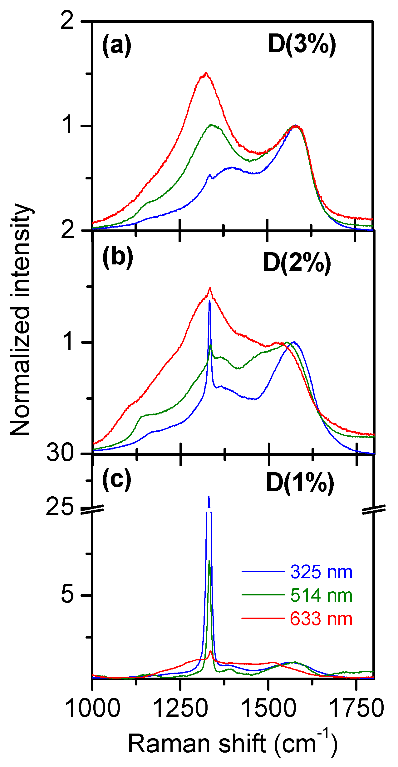
Abstract
:1. Introduction
2. Materials and Methods
2.1. Sample Preparation
2.1.1. CVD Diamond
2.1.2. Hydrogenated Amorphous Carbon
2.1.3. Implanted HOPG
2.2. Sample Characterization
2.2.1. Electron Microscopy and EELS Study
2.2.2. Raman Spectroscopy
3. Results
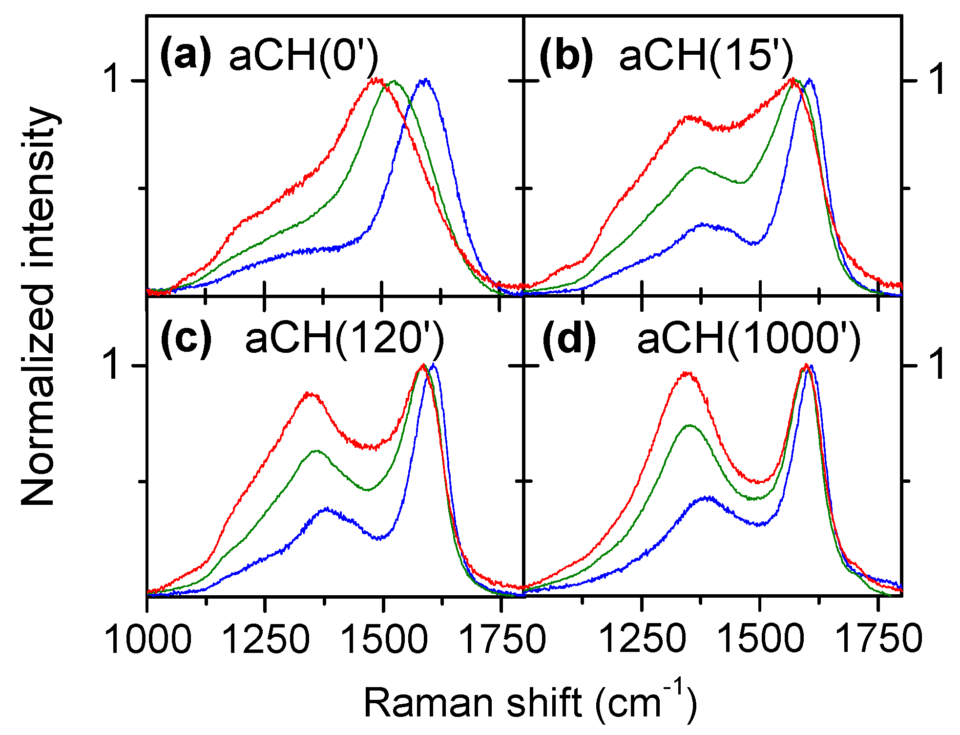
3.1. Multiwavelength Analysis in the 1000–1800 cm−1 Spectral Region
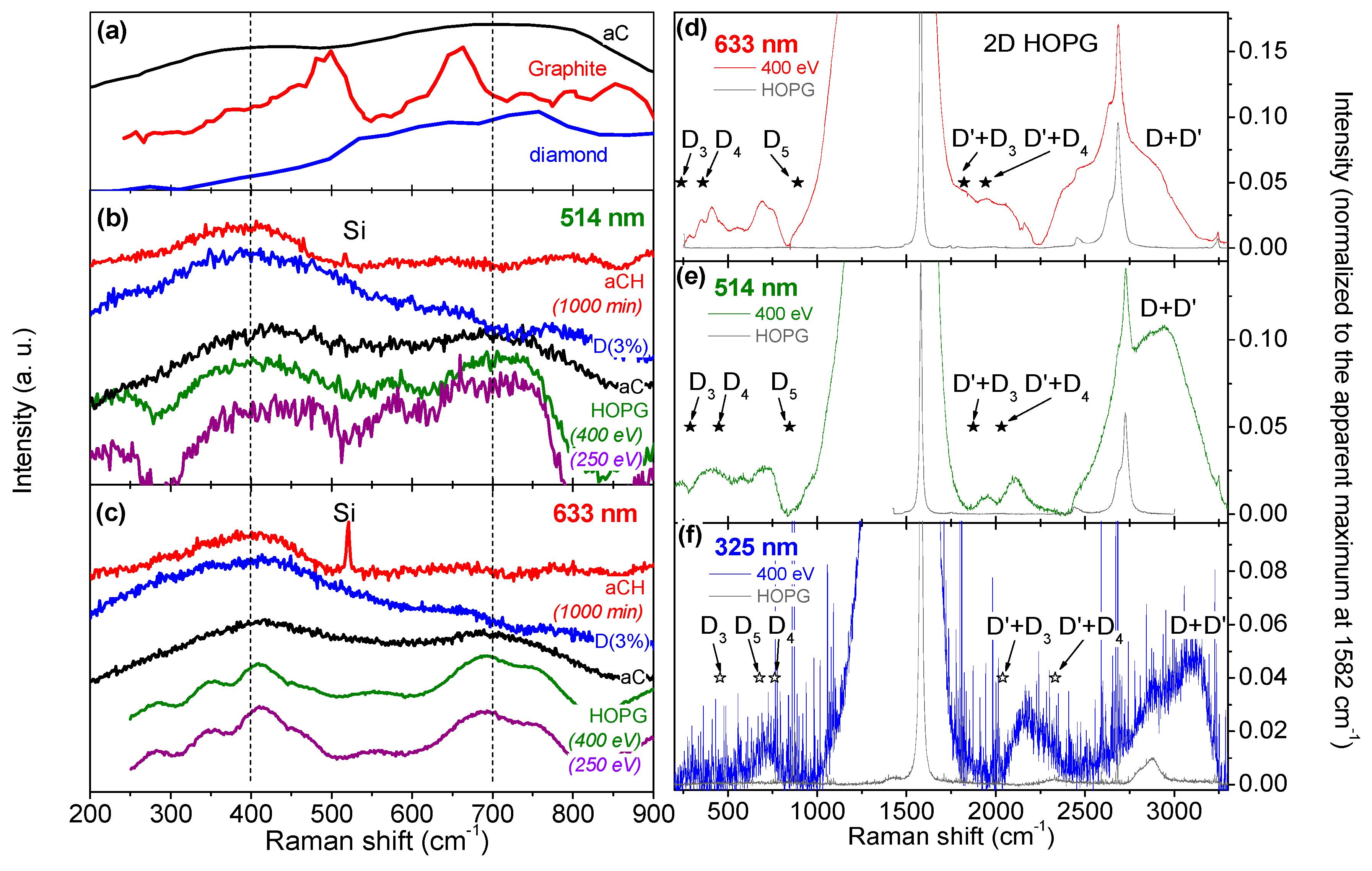
3.2. Multiwavelength Analysis in the PDOS Spectral Region
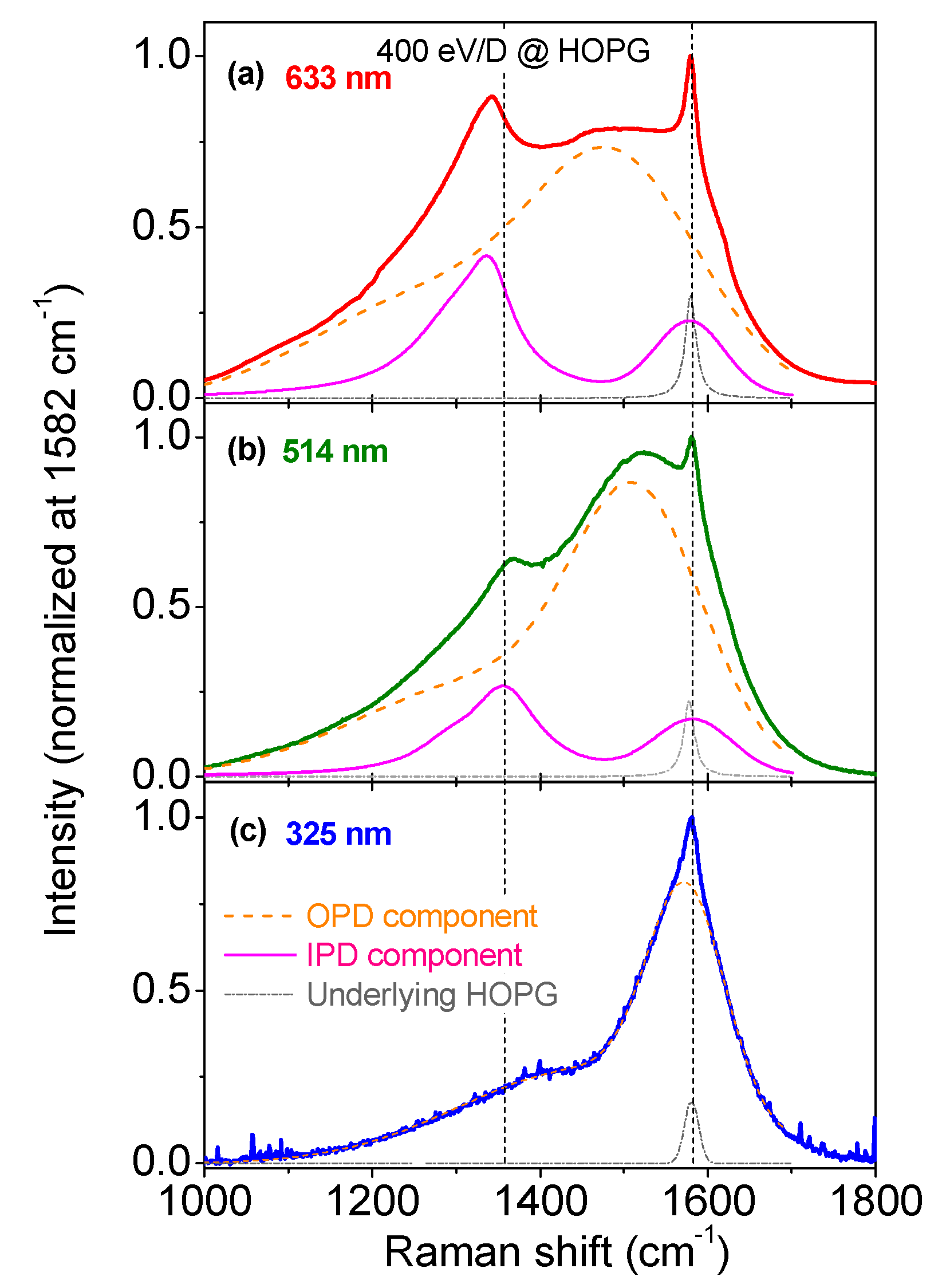
3.3. Multiwavelength Analysis of the Exposed HOPG Samples: Double Resonance Mechanism Evidenced
3.4. Should We Consider the 400 cm−1 Band Height as a New Analysis Tool?
4. Conclusions
Supplementary Materials
Author Contributions
Funding
Acknowledgments
Conflicts of Interest
References
- Merlen, A.; Buijnsters, J.G.; Pardanaud, C. A Guide to and Review of the Use of Multiwavelength Raman Spectroscopy for Characterizing Defective Aromatic Carbon Solids: From Graphene to Amorphous Carbons. Coatings 2017, 7, 153. [Google Scholar] [CrossRef]
- Piscanec, S.; Mauri, F.; Ferrari, A.; Lazzeri, M.; Robertson, J. Ab initio resonant Raman spectra of diamond-like carbons. Diam. Relat. Mater. 2005, 14, 1078–1083. [Google Scholar] [CrossRef]
- Reich, S.; Thomsen, C. Raman spectroscopy of graphite. Philos. Trans. R. Soc. Lond. A 2004, 362, 2271–2288. [Google Scholar] [CrossRef] [PubMed]
- Prawer, S.; Nemanich, R.J. Raman spectroscopy of diamond and doped diamond. Philos. Trans. R. Soc. A Math. Phys. Eng. Sci. 2004, 362, 2537–2565. [Google Scholar] [CrossRef]
- Venezuela, P.; Lazzeri, M.; Mauri, F. Theory of double-resonant Raman spectra in graphene: Intensity and line shape of defect-induced and two-phonon bands. Phys. Rev. B 2011, 84, 035433. [Google Scholar] [CrossRef]
- Meunier, V.; Filho, A.G.S.; Barros, E.B.; Dresselhaus, M.S. Physical properties of low-dimensional sp2-based carbon nanostructures. Rev. Mod. Phys. 2016, 88, 025005. [Google Scholar] [CrossRef]
- Ferrari, A.C.; Robertson, J. Interpretation of Raman spectra of disordered and amorphous carbon. Phys. Rev. B 2000, 61, 14095. [Google Scholar] [CrossRef]
- Ferrari, A.C.; Robertson, J. Resonant Raman spectroscopy of disordered, amorphous, and diamondlike carbon. Phys. Rev. B 2001, 64, 075414. [Google Scholar] [CrossRef]
- Ferrari, A.C.; Robertson, J. Raman spectroscopy of amorphous, nanostructured, diamond-like carbon, and nanodiamon. Philos. Trans. R. Soc. Lond. A 2004, 362, 2477. [Google Scholar] [CrossRef]
- Kuzmany, H.; Pfeiffer, R.; Salk, N.; Günther, B. The mystery of the 1140 cm−1 Raman line in nanocrystalline diamond films. Carbon 2004, 42, 911–917. [Google Scholar] [CrossRef]
- Arenal, R.; Montagnac, G.; Bruno, P.; Gruen, D.M. Multiwavelength Raman spectroscopy of diamond nanowires present in n-type ultrananocrystalline films. Phys. Rev. B 2007, 76, 245316. [Google Scholar] [CrossRef]
- Mermoux, M.; Chang, S.; Girard, H.A.; Arnault, J.-C. Raman spectroscopy study of detonation nanodiamond. Diam. Relat. Mater. 2018, 87, 248–260. [Google Scholar] [CrossRef]
- Puech, P.; Plewa, J.-M.; Mallet-Ladeira, P.; Monthioux, M. Spatial confinement model applied to phonons in disordered graphene-based carbons. Carbon 2016, 105, 275–281. [Google Scholar] [CrossRef]
- Couzi, M.; Bruneel, J.-L.; Talaga, D.; Bokobza, L. A multi wavelength Raman scattering study of defective graphitic carbon materials: The first order Raman spectra revisited. Carbon 2016, 107, 388–394. [Google Scholar] [CrossRef]
- Arenal, R.; Liu, A.C.Y. Clustering of aromatic rings in near-frictionless hydrogenated amorphous carbon films probed using multiwavelength Raman spectroscopy. Appl. Phys. Lett. 2007, 91, 211903. [Google Scholar] [CrossRef]
- Pardanaud, C.; Martin, C.; Roubin, P.; Giacometti, G.; Hopf, C.; Schwarz-Selinger, T.; Jacob, W. Raman spectroscopy investigation of the H content of heated hard amorphous carbon layers. Diam. Relat. Mater. 2013, 34, 100–104. [Google Scholar] [CrossRef]
- Pardanaud, C.; Martin, C.; Cartry, G.; Ahmad, A.; Schiesko, L.; Giacometti, G.; Carrere, M.; Roubin, P. In-plane and out-of-plane defects of graphite bombarded by H, D and He investigated by atomic force and Raman microscopies. J. Raman Spectrosc. 2015, 46, 256–265. [Google Scholar] [CrossRef]
- Casari, C.S.; Bassi, A.L.; Baserga, A.; Ravagnan, L.; Piseri, P.; Lenardi, C.; Tommasini, M.; Milani, A.; Fazzi, D.; Bottani, C.E.; et al. Low-frequency modes in the Raman spectrum of sp-sp2 nanostructured carbon. Phys. Rev. B 2008, 77, 195444. [Google Scholar] [CrossRef]
- Merkulov, V.I.; Lannin, J.S.; Munro, C.H.; Asher, S.A.; Veerasamy, V.S.; Milne, W.I. uv studies of tetrahedral bonding in diamondlike amorphous carbon. Phys. Rev. Lett. 1997, 78, 4869–4872. [Google Scholar] [CrossRef]
- Gilkes, K.W.R.; Prawer, S.; Nugent, K.W.; Robertson, J.; Sands, H.S.; Lifshitz, Y.; Shi, X. Direct quantitative detection of the sp3 bonding in diamond-like carbon films using ultraviolet and visible Raman spectroscopy. J. Appl. Phys. 2000, 87, 7283–7289. [Google Scholar] [CrossRef]
- Chen, Z.Y.; Zhao, J.P.; Yano, T.; Ooie, T.; Yoneda, M.; Sakakibara, J. Observation of sp3 bonding in tetrahedral amorphous carbon using visible Raman spectroscopy. J. Appl. Phys. 2000, 88, 2305–2308. [Google Scholar] [CrossRef]
- Bosak, A.; Krisch, M. Phonon density of states probed by inelastic X-ray scattering. Phys. Rev. B 2005, 72, 224305. [Google Scholar] [CrossRef]
- Wirtz, L.; Rubio, A. The phonon dispersion of graphite revisited. Solid State Commun. 2004, 131, 141–152. [Google Scholar] [CrossRef]
- Kumagai, T.; Choi, J.; Izumi, S.; Kato, T. Structures and phonon properties of nanoscale fractional graphitic structures in amorphous carbon determined by molecular simulations. J. Appl. Phys. 2010, 107, 104307. [Google Scholar] [CrossRef]
- Dmitriev, S.V.; Baimova, J.A.; Savin, A.V.; Kivshar, Y.S. Ultimate strength, ripples, sound velocities, and density of phonon states of strained graphene. Comput. Mater. Sci. 2012, 53, 194–203. [Google Scholar] [CrossRef]
- Cong, X.; Li, Q.-Q.; Zhang, X.; Lin, M.-L.; Wu, J.-B.; Liu, X.-L.; Venezuela, P.; Tan, P.-H. Probing the acoustic phonon dispersion and sound velocity of graphene by Raman spectroscopy. Carbon 2019, 149, 19–24. [Google Scholar] [CrossRef]
- Si, C.; Sun, Z.; Liu, F. Strain engineering of graphene: A review. Nanoscale 2016, 8, 3207–3217. [Google Scholar] [CrossRef]
- Li, Y.; Li, Z.; Shen, P.K. Simultaneous Formation of Ultrahigh Surface Area and Three-Dimensional Hierarchical Porous Graphene-Like Networks for Fast and Highly Stable Supercapacitors. Adv. Mater. 2013, 25, 2474–2480. [Google Scholar] [CrossRef]
- Baig, N.; Saleh, T.A. Electrodes modified with 3D graphene composites: A review on methods for preparation, properties and sensing applications. Microchim. Acta 2018, 185, 283. [Google Scholar] [CrossRef]
- Ferrari, A.C.; Bassi, A.L.; Tanner, B.K.; Stolojan, V.; Yuan, J.; Brown, L.M.; Rodil, S.E.; Kleinsorge, B.; Robertson, J. Density, sp3fraction, and cross-sectional structure of amorphous carbon films determined by X-ray reflectivity and electron energy-loss spectroscopy. Phys. Rev. B 2000, 62, 11089–11103. [Google Scholar] [CrossRef]
- Lajaunie, L.; Pardanaud, C.; Martin, C.; Puech, P.; Hu, C.; Biggs, M.; Arenal, R. Advanced spectroscopic analyses on a:C-H materials: Revisiting the EELS characterization and its coupling with multi-wavelength Raman spectroscopy. Carbon 2017, 112, 149–161. [Google Scholar] [CrossRef] [Green Version]
- Buijnsters, J.; Vázquez, L.; Ter Meulen, J. Substrate pre-treatment by ultrasonication with diamond powder mixtures for nucleation enhancement in diamond film growth. Diam. Relat. Mater. 2009, 18, 1239–1246. [Google Scholar] [CrossRef]
- Hopf, C.; Von Keudell, A.; Jacob, W. The influence of hydrogen ion bombardment on plasma-assisted hydrocarbon film growth. Diam. Relat. Mater. 2003, 12, 85–89. [Google Scholar] [CrossRef]
- Hopf, C.; Angot, T.; Aréou, E.; Dürbeck, T.; Jacob, W.; Martin, C.; Pardanaud, C.; Roubin, P.; Schwarz-Selinger, T. Characterization of temperature-induced changes in amorphous hydrogenated carbon thin films. Diam. Relat. Mater. 2013, 37, 97–103. [Google Scholar] [CrossRef] [Green Version]
- Ahmad, A.; Dubois, J.; Pasquet, T.; Carrere, M.; Layet, J.M.; Faure, J.B.; Cartry, G.; Kumar, P.; Minea, T.; Mochalskyy, S.; et al. Negative-ion surface production in hydrogen plasmas: Modeling of negative-ion energy distribution functions and comparison with experiments. Plasma Sources Sci. Technol. 2013, 22, 25006. [Google Scholar] [CrossRef] [Green Version]
- Schiesko, L.; Carrere, M.; Cartry, G.; Layet, J.M. H—Production on a graphite surface in a hydrogen plasma. Plasma Sources Sci. Technol. 2008, 17, 35023. [Google Scholar] [CrossRef]
- Buijnsters, J.G.; Vázquez, L. Growth Dynamics of Nanocrystalline Diamond Thin Films Deposited by Hot Filament Chemical Vapor Deposition: Influence of Low Sticking and Renucleation Processes. J. Phys. Chem. C 2011, 115, 9681–9691. [Google Scholar] [CrossRef]
- Castro, M.; Cuerno, R.; Nicoli, M.; Vazquez, L.; Buijnsters, J.G. Universality of cauliflower-like fronts: From nanoscale thin films to macroscopic plants. N. J. Phys. 2012, 14, 103039. [Google Scholar] [CrossRef] [Green Version]
- Pardanaud, C.; Martin, C.; Roubin, P. Multiwavelength Raman spectroscopy analysis of a large sampling of disordered carbons extracted from the Tore Supra tokamak. Vib. Spectrosc. 2014, 70, 187–192. [Google Scholar] [CrossRef] [Green Version]
- Popov, M.; Churkin, V.; Kirichenko, A.; Denisov, V.; Ovsyannikov, D.; Kulnitskiy, B.; Perezhogin, I.; Aksenenkov, V.; Blank, V. Raman Spectra and Bulk Modulus of Nanodiamond in a Size Interval of 2–5 nm. Nanoscale Res. Lett. 2017, 12, 561. [Google Scholar] [CrossRef] [Green Version]
- Pardanaud, C.; Aréou, E.; Martin, C.; Ruffe, R.; Angot, T.; Roubin, P.; Hopf, C.; Schwarz-Selinger, T.; Jacob, W. Raman micro-spectroscopy as a tool to measure the absorption coefficient and the erosion rate of hydrogenated amorphous carbon films heat-treated under hydrogen bombardment. Diam. Relat. Mater. 2012, 22, 92–95. [Google Scholar] [CrossRef] [Green Version]
- Pardanaud, C.; Martin, C.; Giacometti, G.; Mellet, N.; Pégourié, B.; Roubin, P. Thermal stability and long term hydrogen/deuterium release from soft to hard amorphous carbon layers analyzed using in-situ Raman spectroscopy. Comparison with Tore Supra deposits. Thin Solid Films 2015, 581, 92–98. [Google Scholar] [CrossRef] [Green Version]
- Levshov, D.; Than, T.X.; Arenal, R.; Popov, V.N.; Parret, R.; Paillet, M.; Jourdain, V.; Zahab, A.A.; Michel, T.; Yuzyuk, Y.I.; et al. Experimental Evidence of a Mechanical Coupling between Layers in an Individual Double-Walled Carbon Nanotube. Nano Lett. 2011, 11, 4800–4804. [Google Scholar] [CrossRef]
- Picher, M.; Anglaret, E.; Arenal, R.; Jourdain, V. Processes Controlling the Diameter Distribution of Single-Walled Carbon Nanotubes during Catalytic Chemical Vapor Deposition. ACS Nano 2011, 5, 2118–2125. [Google Scholar] [CrossRef]
- Arenal, R.; Ferrari, A.C.; Reich, S.; Wirtz, L.; Mevellec, J.-Y.; Lefrant, S.; Rubio, A.; Loiseau, A. Raman Spectroscopy of Single-Wall Boron Nitride Nanotubes. Nano Lett. 2006, 6, 1812–1816. [Google Scholar] [CrossRef]
- Gross, K.; Barragán, J.J.P.; Sangiao, S.; De Teresa, J.M.; Lajaunie, L.; Arenal, R.; Calderón, H.A.; Prieto, P. Electrical conductivity of oxidized-graphenic nanoplatelets obtained from bamboo: Effect of the oxygen content. Nanotechnology 2016, 27, 365708. [Google Scholar] [CrossRef] [Green Version]


© 2019 by the authors. Licensee MDPI, Basel, Switzerland. This article is an open access article distributed under the terms and conditions of the Creative Commons Attribution (CC BY) license (http://creativecommons.org/licenses/by/4.0/).
Share and Cite
Pardanaud, C.; Cartry, G.; Lajaunie, L.; Arenal, R.; Buijnsters, J.G. Investigating the Possible Origin of Raman Bands in Defective sp2/sp3 Carbons below 900 cm−1: Phonon Density of States or Double Resonance Mechanism at Play? C 2019, 5, 79. https://doi.org/10.3390/c5040079
Pardanaud C, Cartry G, Lajaunie L, Arenal R, Buijnsters JG. Investigating the Possible Origin of Raman Bands in Defective sp2/sp3 Carbons below 900 cm−1: Phonon Density of States or Double Resonance Mechanism at Play? C. 2019; 5(4):79. https://doi.org/10.3390/c5040079
Chicago/Turabian StylePardanaud, Cedric, Gilles Cartry, Luc Lajaunie, Raul Arenal, and Josephus Gerardus Buijnsters. 2019. "Investigating the Possible Origin of Raman Bands in Defective sp2/sp3 Carbons below 900 cm−1: Phonon Density of States or Double Resonance Mechanism at Play?" C 5, no. 4: 79. https://doi.org/10.3390/c5040079