1. Introduction
Multilayer structures consisting of alternating layers with different properties have found a wide range of applications in fields like material science, electronics, and optics. Multilayer systems made of alternating high-Z (absorber) and low-Z (spacer) materials can be tailored to act as X-ray mirrors with applications in X-ray astronomy, microscopy, or lithography. The reflectance performance of such multilayer mirrors depends on several parameters, such as contrast in the refractive index/density of paired materials, bilayer period, the thickness ratio of bilayer components, and the quality of interfaces [
1,
2,
3].
Apart from the general rule (based on Z) for choosing X-ray mirror materials, it is also important to use materials with a high difference in refractive index.
The current literature presents several material pairs investigated for applications in X-ray optics, including W/Si [
4], Pt/C [
5], Ni/SiC [
6], Ir/B
4C [
7], W/B
4C [
8], and W/Sc [
9]. Many authors observed interlayer mixing between the used pair materials, and have therefore involved separation/barrier layers from low-segregation materials. Emprin et al. [
6] used W to improve the X-ray reflectivity (XRR) of Ni/SiC multilayers. Although multilayer performance was not improved by the addition of W barrier layers, the authors showed very good agreement between modelled and experiment XRR results. Other authors used C or B
4C to separate the layers, and observed an improvement of reflection [
10].
The type of materials to be chosen is only one of the many aspects to consider when selecting potential materials for the synthesis of X-ray mirrors. In order to obtain quality multilayer structures, sharp interfaces and densities close to bulk values are also necessary. Such properties depend on the deposition technique and, more specifically, on deposition parameters such as ion energy, deposition rate, and substrate temperature. Therefore, a large effort is currently globally made to optimize materials and deposition methods.
The present work is aimed at assessing, for the first time, the potential of a high-voltage anodic-plasma coating technique to fabricate high-quality multilayers for X-ray mirror applications. The choice of materials was made considering the high–low Z requirement.
2. Materials and Methods
Nanolayers of tungsten and silicon were deposited onto 25 × 25 mm2 float-glass substrates in mono-, bi-, and multilayers using a high-voltage anodic-plasma (HVAP) coating system based on thermionic-vacuum-arc (TVA) plasma. Prior to deposition, float-glass substrates were cleaned in a bath of heated (60 °C) isopropyl alcohol for 4 min, and dried in a nitrogen flow.
The high-voltage plasma source worked under high vacuum (10
−6 Torr), and consisted of a hot filament (the cathode) and a crucible containing the deposition material (as anode). The cathode was grounded; while on the anode, a positive bias was applied. More details about the method, different electrode configurations, and plasma characteristics are presented elsewhere [
11,
12,
13,
14].
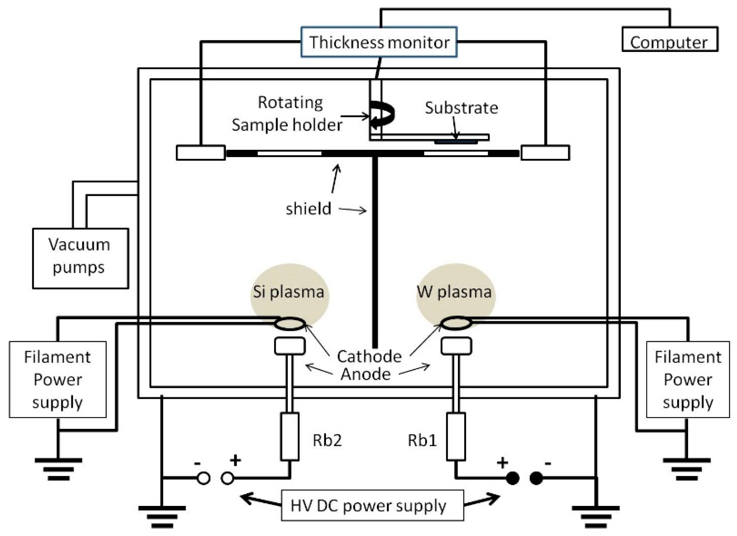
The experiment setup used for nanolayer deposition is presented in
Figure 1. It consisted of two plasma sources with a W and an Si anode, respectively, placed 20 cm apart, and a rotary sample holder mounted 34 cm above the anodes. The ensemble also contained a separation wall between the two plasma sources, and a horizontal plate with windows above each plasma source. The wall and plate were placed in a T shape above the two plasma sources. The sample was moved from above one source to above the other, just in front of the horizontal windows. Thus, no cross-contamination was possible.
The thickness of the deposited films was monitored in situ using quartz microbalance XTC INFICON (New York, NY, USA). Thickness calibration was performed on the basis of XRR measurements (details are presented later in this section).
X-ray reflectivity measurements were performed on a Brucker AXS D8 ADVANCE-type X-ray diffractometer (Karlsruhe, Germany) with a Cu X-ray generator operated at 40 kV and 40 mA, and with a curved multilayer focusing mirror on the incident beam also partially acting as a monochromator for Cu Kα1,2. Beam divergence on the diffracted beam was tailored using a double-slit system with slits of 0.2 or 0.6 mm separated at 100 mm distance from each other in front of a Tl:NaI scintillation counter. Layer thickness, roughness, and density were deduced by modeling the XRR experiment data using the Leptos v4.02 Bruker AXS GmbH software package (Karlsruhe, Germany).
3. Results
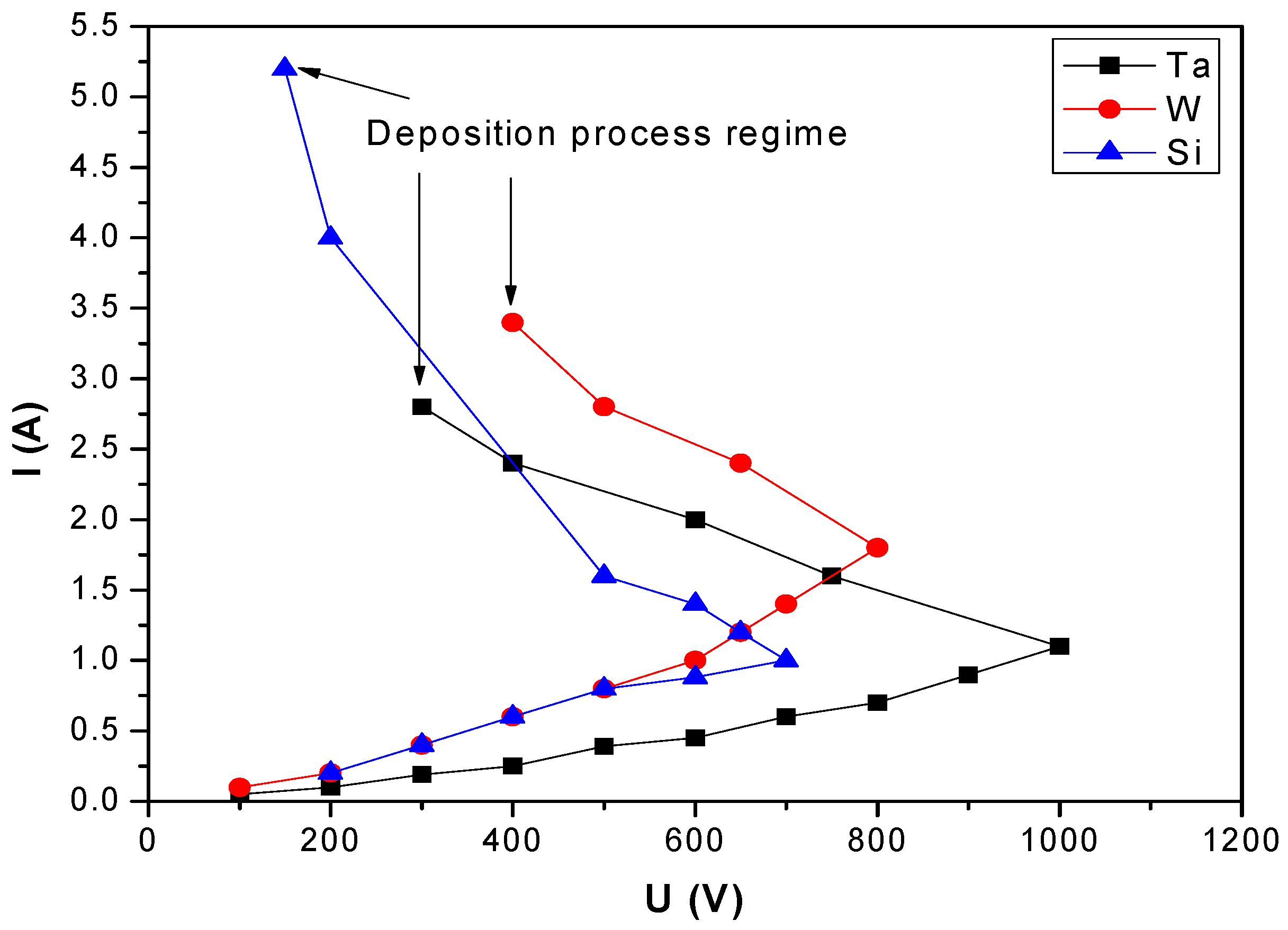
Typical current-voltage characteristics of plasma ignited in W, Ta, and Si vapors showed a slow increase of the current with applied voltage up to the ignition point, where a sudden voltage drop and a simultaneous increase in discharge current was observed (
Figure 2). By further increasing the applied voltage, the plasma current continued to rise. The stable values of current and voltage during deposition depended on a combination of parameters, with the most important being the melting temperature of anode material, cathode–anode distance, and filament current.
3.1. Monolayers
The first step of the work was to determine the minimal layer thickness at which a deposited film becomes continuous. Determining film continuity is not trivial. Abrupt changes of either density or roughness were considered as potential candidates in this respect, as shown in the next section. A criterion for determining the onset of film continuity is proposed.
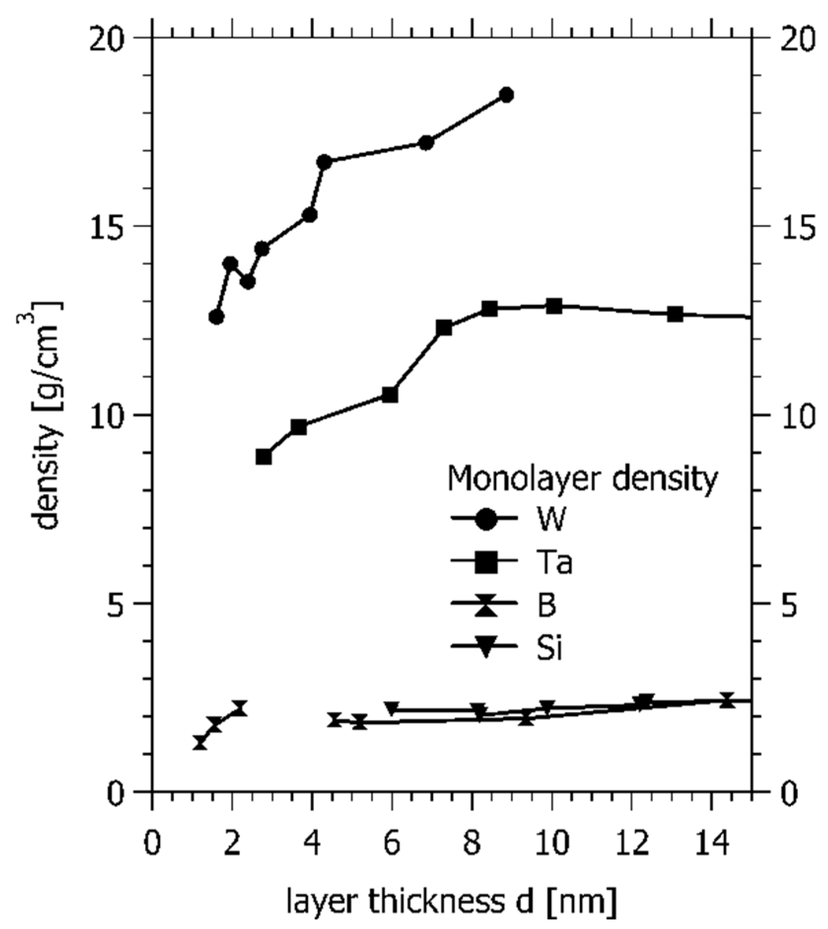
Using the lowest deposition rates for each of the target materials, monolayers of increasing thickness were deposited, and thickness, density, and roughness were plotted against thickness.
Tungsten (W), tantalum (Ta), boron (B), and silicon (Si) monolayers of thicknesses in the 1–20 nm range were deposited on float glass.
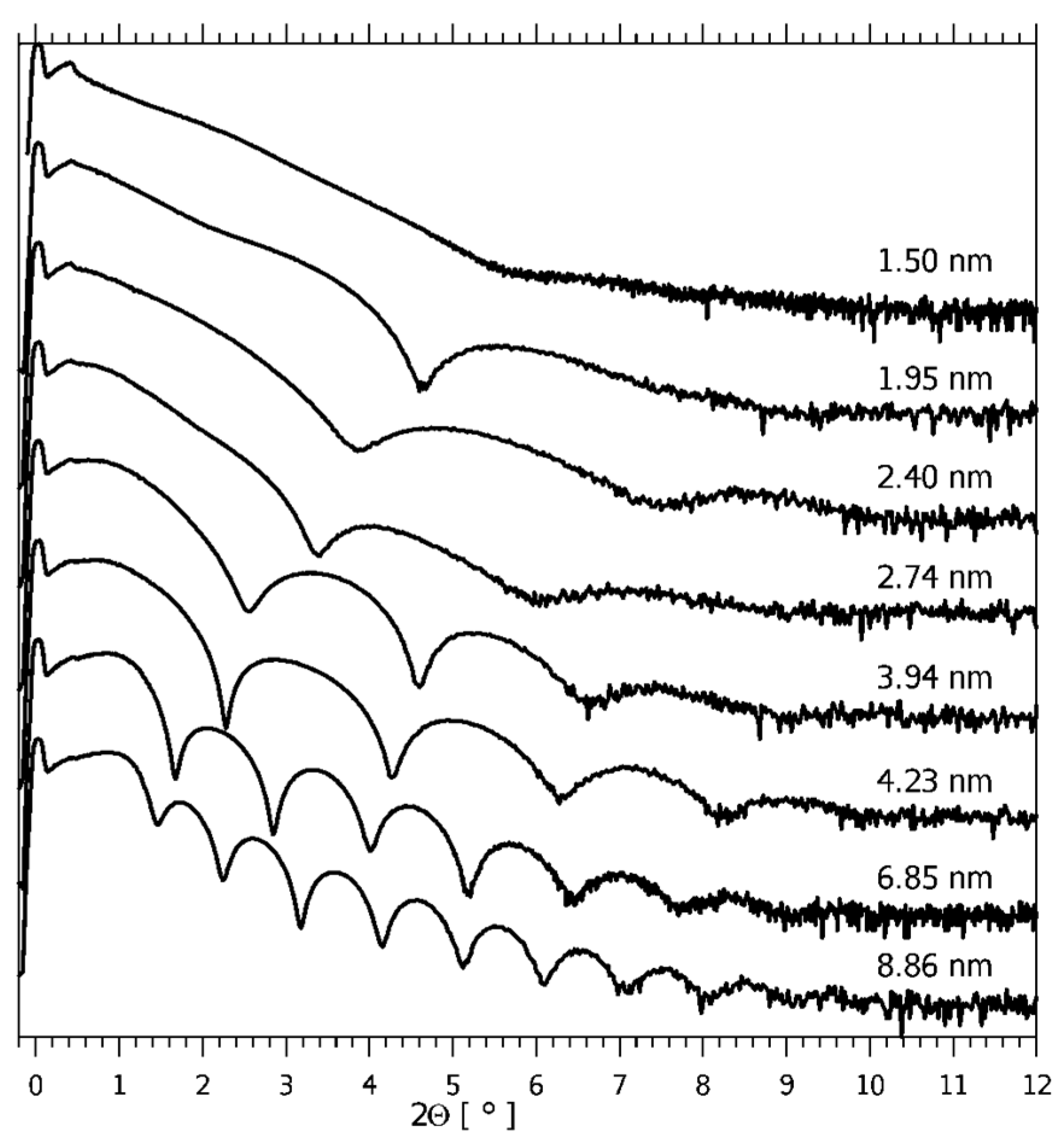
In the case of W monolayers, XRR oscillations built up for all layer thicknesses, and started fading out at around 2θ = 9° for the thickest film (
Figure 3). Critical angle for W films 2θ
W = 1.2° became distinct only at a layer thickness of 8.8 nm. Minimal film thickness for continuous films for the studied metals was 4 nm (W), 6 nm (Ta), 2.5 nm (B), and 6 nm (Si).
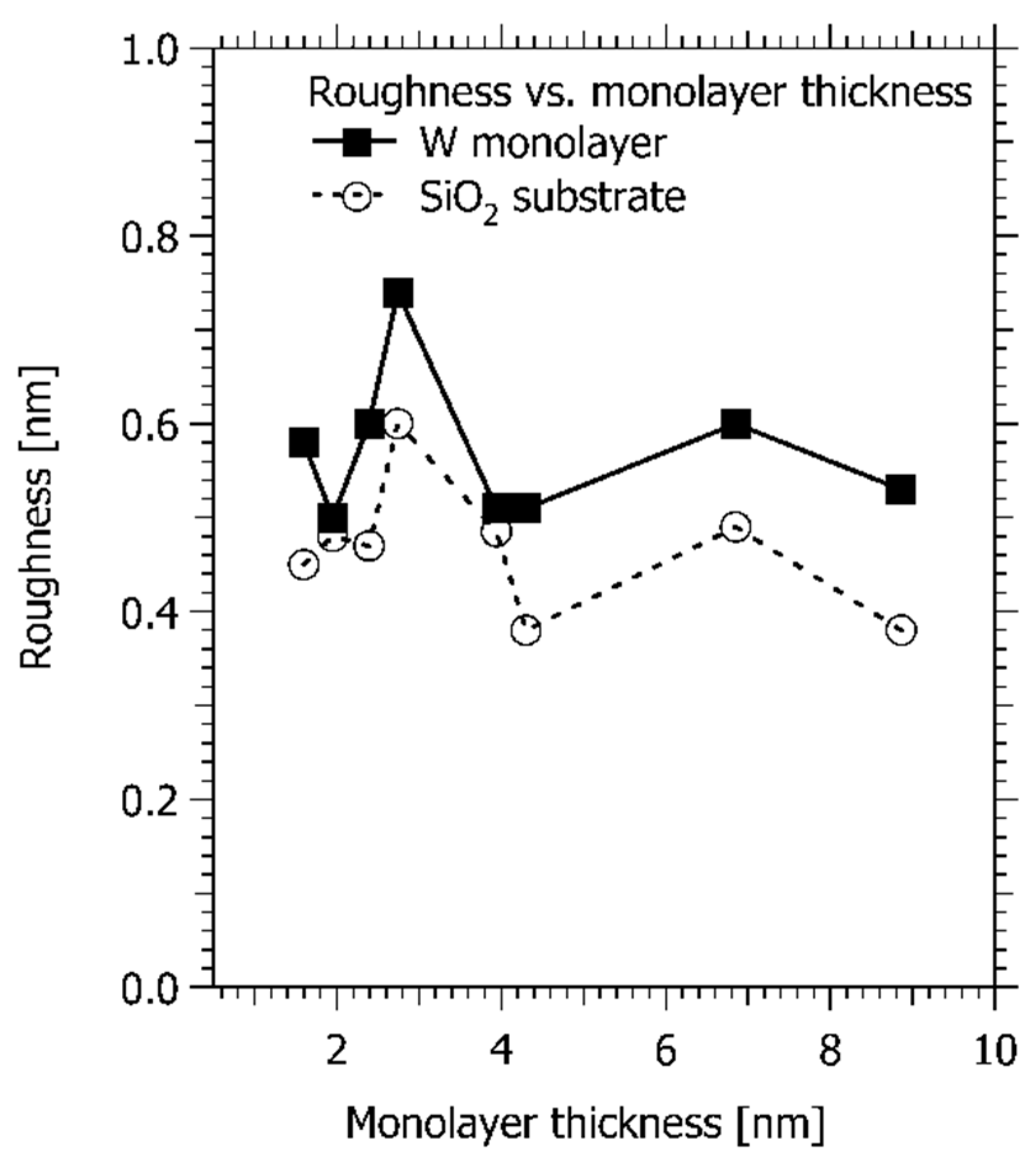
The plot of roughness vs. monolayer thickness (
Figure 4) shows that float-glass-substrate roughness was in the range of 0.45–0.6 nm, and the roughness value of the W monolayer was only about 0.1 nm higher, with an average value of 0.57 ± 0.06 nm. Similar behavior was observed in the case of the Ta (
R = 0.58 ± 0.1 nm), B (
R = 0.58 ± 0.1 nm), and Si (
R = 0.45 ± 0.11 nm) monolayers. The fact that roughness values remained basically constant with layer thickness suggested that the island mode growth mechanism governed our thin-film deposition process, and roughness could not be used to determine the onset of continuity for layer thickness. Nevertheless, the plot of layer density versus layer thickness (see
Figure 5) revealed an increase in density up to a threshold point from where it remained constant. In the case of heavy element materials such as W and Ta, the onset of constant density occurred at a film thickness of about 6–8 nm. For lighter elements Si and B, such a point was achieved at a lower film thickness, at about 2 nm. The threshold point can be regarded as a criterion for establishing the minimal film thickness necessary for the film to become continuous.
3.2. Bilayers
In order to study phenomena at the interface of two layers of differing composition, a set of W–B and W–Si bilayers were deposited.
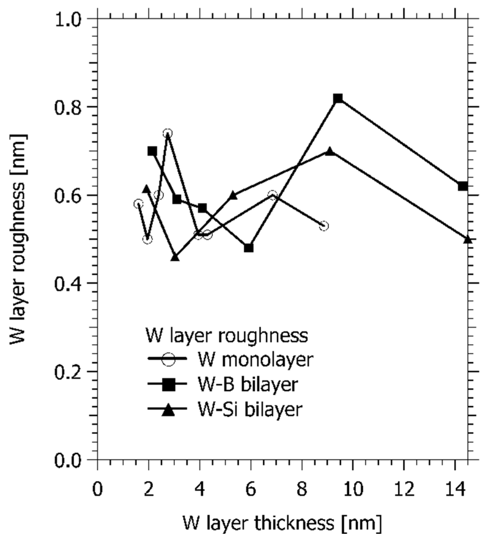
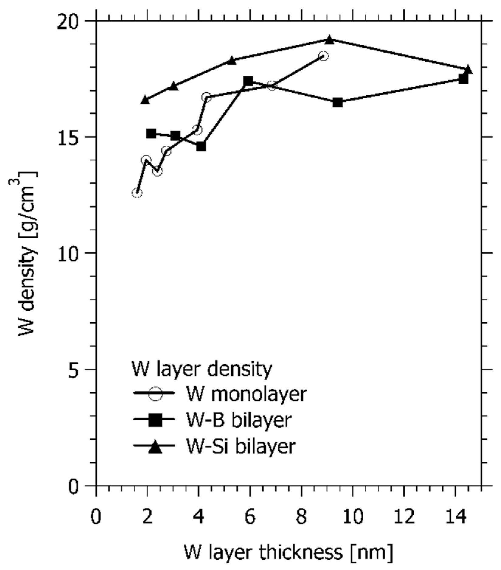
A study of the change of W nanofilm roughness and density with W film thickness, either as monolayer or in bilayers, was undertaken. W film thickness was increased from 3 to 14 nm, and the top B or Si layer thickness was chosen to be large enough to be continuous (10–20 nm). Roughness and density values of the W layers as modelled by XRR were not affected by the top-layer deposition of the B or Si layer (see
Figure 6 and
Figure 7). Average roughness for the W layer remained at about 0.6 nm, and density vs. thickness dependence for the W layer in the W–B or W–Si bilayer structures had similar dependence as that in the case of W monolayers.
As neither roughness nor density of W nanolayers was significantly affected by the deposition of the Si or B top layer, we concluded that both spacer materials were eligible for further multilayer deposition. Using these results, we proceeded to synthesize and analyze periodical multilayer test structures.
3.3. Multilayers
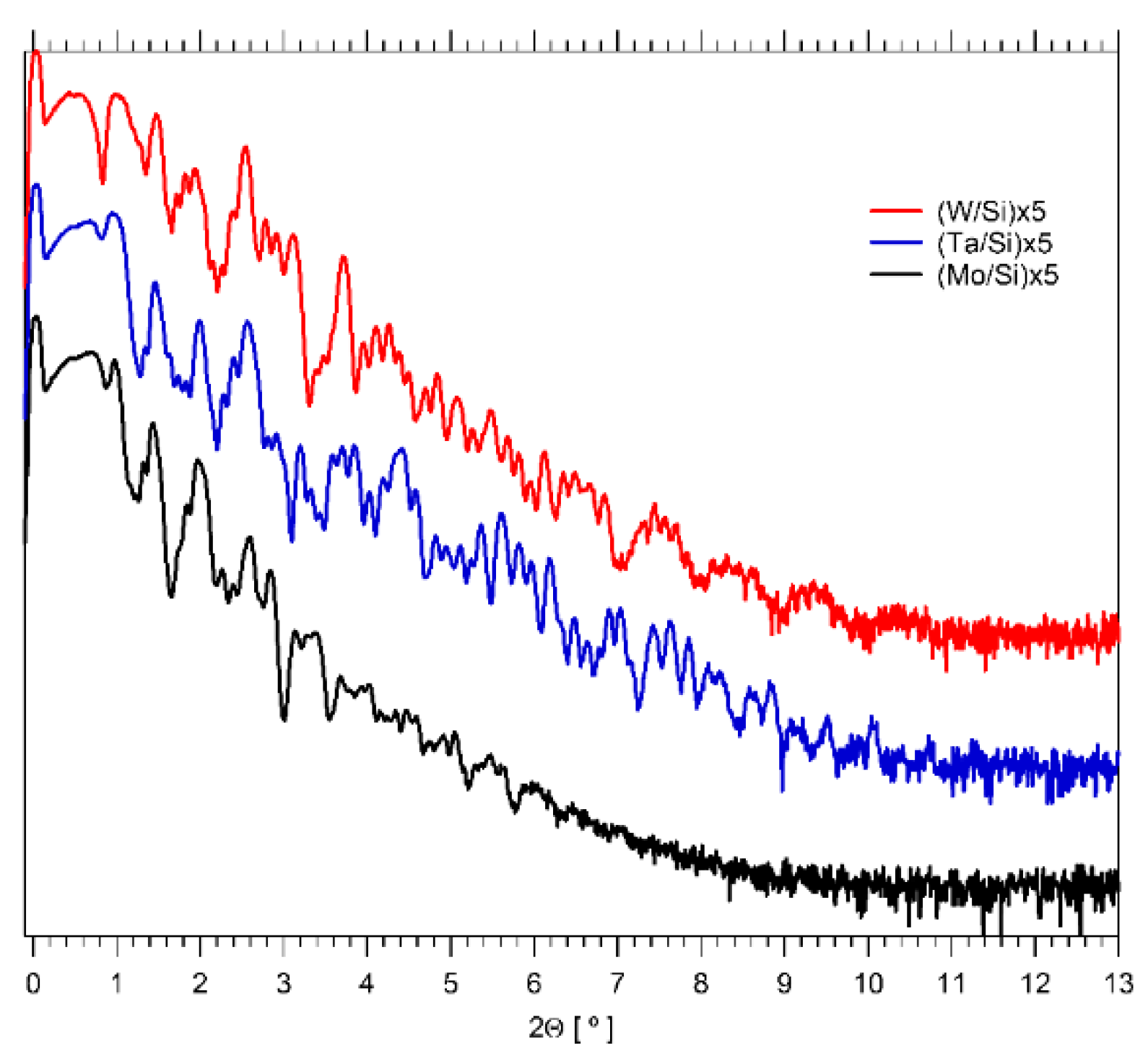
In order to assess the extent of interlayer mixing phenomena, a series of multilayers containing five bilayer test structures were deposited using the HVAP technique.
XRR spectra of some test structures having an Si spacer and W, Ta, and Mo reflector films are presented in
Figure 8. As can be observed in this figure, reflectivity oscillations of the 5× Mo–Si bilayer test structure started to fade out at reflection angles of 2θ = 6°, while in the case of the 5× Ta–Si and 5× W–Si bilayer structures, oscillations were quenched at a higher angle of 2θ = 10–11°. The first- and second-periodical-order reflections had relative intensities compared to the half-beam intensities. These aspects already showed that the 5× W–Si bilayer test structure had overall higher reflectivity performance compared to that of the other two. In order to understand the underlying reasons of this result, we compared the modelled XRR data.
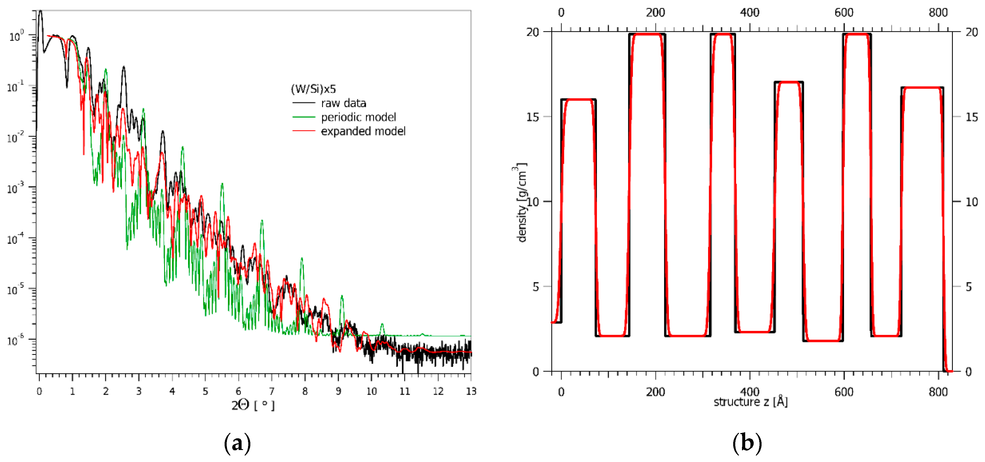
Figure 9a presents the raw data of a 5× W/Si multilayer with two modelled XRR spectra. Depending on the starting model, XRR modeling can lead to several solutions that all give a “best fit”, and no unique solution can be ensured. However, starting from simple structures with a small number of layers, one can develop models that then apply for structures with a larger number of layers. In our case, we started modeling with perfect periodic-structure models, and the obtained average values for layer thickness, density, and roughness were then used to fit each layer for the entire structure. In the following, we named the two structure models “periodic” and “expanded”. Comparing the two models helped to evaluate how close the expanded model was to the perfect periodic.
As can be seen in
Figure 9b, a dispersion of thickness and density was obtained for the W–Si deposited stack of layers. This result was contrary to our expectation, as the deposition was made under identical plasma parameters, namely, an arc current of 5.2 A and arc voltage of 150 V. Calculated average layer thickness for Si was
davg(Si) = 7.16 ± 0.62 nm, with a relative error of 8%,
davg(W) = (4.64 ± 0.53) nm for W, with a relative error of 10%. Deduced average density for Si was 2.6 ± 0.91 g/cm
3 with a relative error of 20%, while this value was 19.60 ± 1.98 g/cm
3 for W, with a relative error of 13%.
Analyzing the deposition process, we realized that there was a series of issues affecting the quality of the obtained multilayer structure. One was related to the fact that, by alternatively turning the two plasma sources on and off, a variation of anode temperature takes place, resulting in a change in deposition rate even when using the same electrical parameters of the plasma. While deposition of monolayers and bilayers in the precedent studies could be started after the anode reached a steady temperature, in the case of multilayers, deposition was run as soon as the plasma reached the desired electrical parameters. Otherwise, the time needed to obtain the thermal stability of the anode each time a nanolayer was deposited would have been too long and impractical.
Variation in nanolayer thickness was also due to errors introduced by the manual operation of the shutter after each deposition.
An important aspect in relation to the imperfection in reproducing fixed thicknesses and densities of nanolayers in a multilayer stack was related to the use of quartz microbalance for in situ thickness measurement. By this technique, layer thickness was calculated using an ideal layer model where the sensed atoms were uniformly distributed over the quartz surface, without considering the real growth mechanism of the nanolayer (where atoms may deposit on top of the other forming islands). This was detrimental, as real nanolayer-thickness values were not accurately measured in situ. Moreover, using just one quartz microbalance, the quartz was placed between the two plasmas and laterally “saw” the plasma plume, thus introducing errors.
4. Discussion
An aspect related to the monolayer densities of continuous films was the fact that their values were smaller than their corresponding bulk values. In the case of W, this density difference was rather small: 19.6 g/cm3 for an 8.8 nm W continuous layer compared to 19.37 g/cm3 for bulk densities. In the case of lighter elements Si and B, film density was almost equal to the bulk values (2.33 g/cm3 for Si, and 2.21 g/cm3 for B). One notable difference was, however, observed for Ta: 12.65 g/cm3 for a 13 nm Ta layer compared to 16.67 g/cm3 for the bulk material. These differences could have been caused by different crystallization mechanisms during deposition and crystal-grain formation, which will be further investigated in a future study by TEM.
Interlayer mixing caused by the interdiffusion of atoms from consecutive layers can degrade the performance of periodical multilayer structures. Exposure to escalating temperatures during the long deposition processes of such layer structures was found to be an important trigger of interlayer diffusion [
15,
16,
17,
18]. Apart from interlayer mixing, good reproducibility of nanolayer thickness and density was needed for obtaining constructive interference. The values of monolayer roughness obtained in our study were below 0.6 nm for all used materials. This compared well with the current benchmark roughness value of 0.45 nm obtained by a team from the European Space Agency [
7].
Analyzing the deposition process, we realized that there was a series of issues affecting the quality of the obtained multilayer structure. One was related to the fact that, by alternatively turning the two plasma sources on and off, a variation of anode temperature took place, resulting in a change in deposition rate even when using the same electrical parameters of the plasma. While deposition of monolayers and bilayers in the precedent studies could be started after the anode reached a steady temperature, in the case of multilayers, deposition was run as soon as the plasma reached the desired electrical parameters. Otherwise, the time needed to obtain the thermal stability of the anode each time a nanolayer was deposited would have been too long and impractical. Variation in nanolayer thickness was also due to errors introduced by the manual operation of the shutter after each deposition.
The work allowed the identification of advantages and pitfalls of an experiment setup based on the HVAP deposition technique. Further development of the setup includes a computer-controlled system for the alternative exposure of the substrate to the two plasma sources, and the better management of the vacuum with the outgassing of chamber walls and substrates before deposition.
5. Conclusions
The work presented here aimed at assessing the potential of the HVAP source for the synthesis of quality nanolayers for X-ray optics.
A series of monolayers and bilayers were deposited on smooth glass substrates and analyzed by XRR. Results allowed the identification of a criterion for the selection of the minimal nanolayer thickness necessary to obtain film continuity. Nanolayer density increased with thickness in discontinuous films and reached a constant value thereafter. This behavior was observed for all low- and high-Z materials investigated. This indicated an island-growth mechanism of the layers deposited by HVAP.
It was observed that the continuous nanolayers deposited by HVAP had constant density with increasing film thickness. Moreover, for each specific plasma condition, roughness did not build up with film thickness, and could be lowered by decreasing deposition rate. Low roughness values, comparable with the state of the art, were obtained in this work. This suggests that HVAP is a promising deposition technique for X-ray mirrors.
The study also revealed that, for the same electrical parameters of the HVAP plasma, the deposition rate varied until a steady anode temperature is reached. In order to obtain the better control of nanolayer thickness and density in the multilayer, both plasma sources would need to be running for the whole duration of multilayer deposition.
Author Contributions
Conceptualization, A.-M.V. and C.S.-B.; methodology, A.A. and M.B.; software, A.-M.V.; validation, A.-M.V., A.A., and M.B.; formal analysis, C.S.-B.; investigation, A.A.; resources, C.S.-B.; data curation, A.-M.V.; writing—original-draft preparation, A.-M.V.; writing—review and editing, C.S.-B.; supervision, A.-M.V. and C.S.-B.; project administration, C.S.-B.; funding acquisition, C.S.-B. All authors have read and agreed to the published version of the manuscript.
Funding
This research was funded by of the Romanian National Authority for Scientific Research and Innovation, CNCS-UEFISCDI, Grant No. PN-II-RU-TE-269/2015 and NUCLEU contract No. 16N/2019.
Conflicts of Interest
The authors declare no conflict of interest. The funders had no role in the design of the study; in the collection, analyses, or interpretation of data; in the writing of the manuscript, or in the decision to publish the results.
References
- Siewert, F.; Buchheim, J.; Zeschke, T.; Störmer, M.; Falkenberg, G.; Sankari, R. On the characterization of ultra-precise X-ray optical components: Advances and challenges in ex situ metrology. J. Synchrotron Radiat. 2014, 21, 968–975. [Google Scholar] [CrossRef] [PubMed] [Green Version]
- Rack, A.; Assoufid, L.; Lee, W.K.; Shi, B.; Liu, C.; Morawe, C.; Kluender, R.; Conley, R.; Bouet, N. Hard X-ray multilayer mirror round-robin on the wavefront preservation capabilities of W/B4C coatings. Radiat. Phys. Chem. 2012, 81, 1696–1702. [Google Scholar] [CrossRef]
- Morawe, C.; Supruangnet, R.; Peffen, J.C. Structural modifications in Pd/B4C multilayers for X-ray optical applications. Thin Solid Film. 2015, 588, 1–10. [Google Scholar] [CrossRef]
- Wang, F.F.; Mu, B.Z.; Jin, H.J.; Yang, X.J.; Zhu, J.T.; Wang, Z.S. Effect of separating layer thickness on W/Si multilayer replication. Opt. Express 2011, 19, 15929–15936. [Google Scholar] [CrossRef] [PubMed]
- Lodha, G.; Poul, A.; Vitta, S.; Gupta, A.; Nandedkar, R.; Yamashita, K.; Kunieda, H.; Tawara, Y.; Tamura, K.; Haga, K. Study of Pt/C X-ray Multilayer Structure as a Function of Layer Perid Using X-ray Scattering. Jpn. J. Appl. Phys. 1999, 38, 289. [Google Scholar] [CrossRef] [Green Version]
- Emprin, B.; Troussel, P.; Soullie, G.; Stemmler, P.; Mercere, P.; Meltchakov, E.; Jerome, A.; Delmotte, F. X-ray broadband Ni/SiC multilayers: Improvement with W barrier layers. Opt. Express 2014, 22, 25853–25865. [Google Scholar] [CrossRef] [Green Version]
- Della Monica Ferreira, D.; Jakobsen, A.; Massahi, S.; Christensen, F.; Shortt, B.S.; Jørgen, G.; Antoni, T.-R.; Michael, K.; Levent, C.; Stefanie, M. X-ray mirror development and testing for the ATHENA mission. In Space Telescopes and Instrumentation 2016: Ultraviolet to Gamma Ray; SPIE: Cardiff, Wales, 2016. [Google Scholar]
- Jankowski, A.F. W/B4C multilayer X-ray mirrors. Opt. Eng. 1991, 30, 2003. [Google Scholar] [CrossRef]
- Salashchenko, N.N.; Fraerman, A.A.; Mitenin, S.V.; Prokhorov, K.A.; Shamov, E.A. Short-period X-ray multilayers based on Cr/Sc, W/Sc. Nucl. Instrum. Methods Phys. Res. Sect. A Accel. Spectrometers Detect. Assoc. Equip. 1998, 405, 292–296. [Google Scholar] [CrossRef]
- Braun, S.; Mai, H.; Moss, M.; Scholz, R. Microstructure of Mo/Si multilayers with barrier layers. In International Symposium on Optical Science and Technology; SPIE: Cardiff, Wales, 2002; Volume 4782. [Google Scholar]
- Surdu-Bob, I.M.; Iacob, C. General characteristics of the Thermoionic Vacuum Arc plasma. J. Optoelectron. Adv. Mater. 2007, 9, 2932. [Google Scholar]
- Badulescu, M.; Gruia, I.; Surdu-Bob, C.; Iacob, C. Retarding field ion energy analysis of an anodic arc carbon plasma. Optoelectron. Adv. Mater. Rapid Commun. 2009, 12, 1269–1272. [Google Scholar]
- Badulescu, M.; Gruia, I.; Micheli, V.; Calliari, L.; Surdu-Bob, C. Diamond film nano-abrasives obtained by anodic arc. Optoelectron. Adv. Mater. Rapid Commun. 2009, 11, 1207–1209. [Google Scholar]
- Surdu-Bob, C.C.; Racolta, P.M.; Badulescu, M.; Chiojdeanu, C.; Arsene, N.; Logofatu, C.; Ionescu, C.; Sporea, D.; Gruia, I. Pure, smooth and dense W films obtained by an anodic arc plasma. Optoelectron. Adv. Mater. Rapid Commun. 2011, 5, 1336–1340. [Google Scholar]
- Stoev, K.; Sakurai, K. Optimization of the design of a multilayer X-ray mirror for Cu-Kα energy. Jpn. J. Appl. Phys. 2014, 53, 05FH01. [Google Scholar] [CrossRef]
- Soufli, R. Breakthroughs in Photonics 2013: X-ray Optics. IEEE Photonics J. 2014, 6, 1–6. [Google Scholar] [CrossRef]
- Vishnyakov, E.A.; Voronov, D.L.; Gullikson, E.M.; Kondratenko, V.V.; Kopylets, I.A.; Luginin, M.S.; Pirozhkov, A.S.; Ragozin, E.N.; Shatokhin, A.N. Normal-incidence Sb/B4C multilayer mirrors for the 80 Å <λ <120 Å wavelength range. Quantum Electron. 2013, 43, 666–673. [Google Scholar]
- Mahmood, A. Comprehensive Guide for Nanocoatings Technology; Nova Publisher: New York, NY, USA, 2016; Volume 2. [Google Scholar]
© 2020 by the authors. Licensee MDPI, Basel, Switzerland. This article is an open access article distributed under the terms and conditions of the Creative Commons Attribution (CC BY) license (http://creativecommons.org/licenses/by/4.0/).


