Article

The Effect of the Deposition Method on the Structural and Optical Properties of ZnS Thin Films

1
National Institute of Materials Physics, Atomistilor 405A, 077125 Magurele, Romania
2
Faculty of Physics, University of Bucharest, Atomistilor 405, 077125 Magurele, Romania
3
Horia Hulubei National Institute of Physics & Nuclear Engineering, 077125 Magurele, Romania
4
Apel Laser Ltd., Vanatorilor 25, 077135 Mogosoaia, Romania
*
Author to whom correspondence should be addressed.
Coatings 2021, 11(9), 1064; https://doi.org/10.3390/coatings11091064
Submission received: 4 August 2021 / Revised: 31 August 2021 / Accepted: 1 September 2021 / Published: 3 September 2021

Abstract

:
ZnS is a wide band gap material which was proposed as a possible candidate to replace CdS as a buffer layer in solar cells. However, the structural and optical properties are influenced by the deposition method. ZnS thin films were prepared using magnetron sputtering (MS), pulsed laser deposition (PLD), and a combined deposition technique that uses the same bulk target for sputtering and PLD at the same time, named MSPLD. The compositional, structural, and optical properties of the as-deposited and annealed films were inferred from Rutherford backscattering spectrometry, X-ray diffraction, X-ray reflectometry, Raman spectroscopy, and spectroscopic ellipsometry. PLD leads to the best stoichiometric transfer from target to substrate, MS makes fully amorphous films, whereas MSPLD facilitates obtaining the densest films. The study reveals that the band gap is only slightly influenced by the deposition method, or by annealing, which is encouraging for photovoltaic applications. However, sulphur vacancies contribute to lowering the bandgap and therefore should be controlled. Moreover, the results add valuable information towards the understanding of ZnS polymorphism. The combined MSPLD method offers several advantages such as an increased deposition rate and the possibility to tune the optical properties of the obtained thin films.

1. Introduction

Zinc sulfide is an intensively investigated semiconductor material with applications in light emitting diodes [1,2], photonic crystals [3], anti-reflection coatings [4], heterojunction diodes [5], and photovoltaic cells [6,7]. ZnS has low toxicity [8], low cost, and is relatively abundant in nature [9], where it occurs as the mineral called sphalerite [10,11]. It is an n-type semiconductor material with a wide band gap energy [12] at room temperature of ~3.6 eV, which is larger than the bandgap of CdS (2.40 eV) [13], making ZnS a possible candidate as a buffer layer in p-n junctions of solar cells [14], although some compositional engineering should be performed.
ZnS is intriguing due to its polymorphism at room temperature, with two main crystalline structures. One phase is the face-centered cubic lattice, also called a “zinc blende” type structure [15], which belongs to the space group F-43m (216). The second phase is a hexagonal structure, also called “wurtzite ZnS”, with the lattice belonging to the space group P63mc (186). In a zinc blende, each zinc atom is surrounded by four sulfur atoms, and each sulfur atom is surrounded by four zinc atoms in a tetrahedral coordination. On the other hand, wurtzite is characterized by 12 atoms in the corners of each unit that create a hexagonal unit cell [16], which is also tetrahedrally coordinated [15].
Since the zinc blende structure is denser than the wurtzite structure, a transition from zinc blende to wurtzite occurs naturally over time (extremely slow) at a rate similar to the transition of diamond to graphite [16]. However, by thermal treatment, the cubic zinc blende can be transformed into a hexagonal structure (wurtzite) at 1020 °C [10,15].
ZnS thin films have been successfully obtained by a wide variety of deposition techniques such as thermal evaporation [17], molecular beam epitaxy [18,19], sol gel deposition [20], chemical bath deposition [21], pulse laser deposition [22,23], magnetron sputtering [24], or chemical vapor deposition [25].
Magnetron sputtering (MS) deposition is a low cost and efficient technique for the deposition of large area coatings (e.g., 1200 × 3000 mm2 [26]), with tuned deposition rate leading to a good film composition control. Energetic ions of the working gas (usually argon are accelerated by an electric field and hit the target surface, ejecting atoms with sufficient kinetic energy to reach the substrate. The use of a magnetic field (i.e., magnetron sputtering source) confines the ions in the plasma resulting in an increased deposition rate of the sputtered material [27]. MS is widely used to prepare a variety of materials in thin film form such as metals, semiconductors, and insulators, the latter only by radio-frequency assistance. It is worth mentioning the possibility to obtain uniform and smooth films with a strong adhesion to the substrate [28].
Pulsed laser deposition (PLD) is a technique where an intense laser pulse is guided by mirrors through an optical window of a vacuum chamber and is directed onto a target [29]. Above a certain power density, the ablation process occurs. The material ejected from the target is transferred towards the substrate surface. When compared to other thin film deposition methods, PLD has the advantage that, under optimal conditions, the ratios of the elemental components concentration of the target and those of the obtained film are roughly identical, even for ternary (or higher order) targets [30,31]; however, the uniform area is relatively small [32]. The most important disadvantage of PLD is the formation of droplets on the substrate due to the change in melting/evaporation processes on the target surface, thus the laser fluence should be carefully adjusted [33,34].
There have been some published reports on combining MS and PLD for the deposition of carbides and diamond-like carbon films [35], tin oxide films [36], GST-225 [37], and ternary wolfram borides [38]. Simultaneous MS and PLD deposition can lead to a denser film [36] with a smoother surface [38].
The purpose of this research is to compare the structural and optical properties of ZnS thin films obtained by magnetron sputtering, pulsed laser deposition, and combined MSPLD. When combining the two deposition methods, one can expect to obtain thin films which have the advantages of both MS and PLD, namely improved structural, compositional and optical properties and the possible mitigation of their disadvantages such as low deposition rate and area in PLD. Moreover, the present work can add valuable information towards the understanding of ZnS polymorphism.

2. Materials and Methods

Thin films of ZnS were prepared at room temperature on silicon and glass substrates by magnetron sputtering in an argon atmosphere at a pressure of 5 × 10⁻⁵ torr (Linde, Bucharest, Romania). A Gencoa 3G Circular Magnetron (Gencoa, Liverpool, UK) powered by an RF T&C Power Conversion Inc., Model AG 0313 (RF T&C Power Conversion Inc., New York, NY, USA) source was used for MS samples. The substrates have been placed at a distance of 8 cm from the ZnS ceramic target (5 cm in diameter, Mateck GmbH, Jülich, Germany). The deposition rate of 0.1 nm/s at a RF power of 60 W was determined using an Inficon Q-pod calibration software (Inficon, Bad Ragaz, Switzerland) connected to a quartz crystal.
Another set of ZnS films was prepared by PLD, using a 248 nm wavelength KrF laser source (COMPexPro KrF laser, Coherent, Santa Clara, CA, USA). A similar deposition rate of 0.1 nm/s was achieved for a repetition rate of 2 Hz and a laser power of 60 mJ (1.5 J/cm2 fluence).
A third set of ZnS films was deposited by combining both techniques using the above described parameters, leading to an estimated deposition rate of ~0.2 nm/s. The deposition times were adjusted to expect comparable film thicknesses. All the ZnS films were obtained at room temperature, on substrates with a size of 12 × 15 mm2, in the same deposition conditions. The deposition chamber was evacuated down to 4 × 10⁻⁶ Torr and afterwards an Argon flow of 30 sccm per minute was inserted into the deposition chamber. The pressure was kept constant during deposition at 5 × 10⁻³ Torr, for all deposition methods.
ZnS thin films have been annealed in vacuum (7 × 10⁻² Torr) at 400 °C for 1 h using a GSL 1600X furnace (MTI, Richmond, CA, USA) with an increment of 1.5 °C per minute for heating and cooling.
Rutherford backscattering spectrometry (RBS) using alpha particles from a 3 MV Tandetron [39] (3 MV TandetronTV at IFIN-HH, Magurele, Romania) was performed. The SIMNRA® software, package version 7.0 (Max-Planck-Institut für Plasmaphysik, Garching, Germany) [40], was employed for the simulation of the RBS spectra in order to investigate the composition.
Thin films structure investigation was performed by grazing incidence X-ray diffraction (GIXRD) at an incidence angle of 0.4°, using a Rigaku SmartLab diffractometer (Rigaku, Tokyo, Japan) equipped with a HyPix-3000 2D Hybrid Pixel Array Detector (Rigaku, Tokyo, Japan) in “0D” mode. The identification of the crystalline phases was made with the DIFFRAC.SUITE Software, package version 4.2 (Bruker, Billerica, MA, USA). X-ray reflectometry (XRR) in the range 0°–2.3° (2θ) with a step of 0.004° (2θ) was used for thickness and mass density estimation.
The Raman spectra were obtained at room temperature, in the 100–1100 cm−1 range in backscattering configuration, with a LabRAM HR Evolution spectrometer (Horiba Jobin-Yvon, Palaiseau, France) supplied with a confocal microscope. The He–Cd laser (325 nm) (Horiba Jobin-Yvon, Palaiseau, France) was focused using an Olympus 40x objective (Olympus, Tokyo, Japan) on the surface of thin films.
The spectroscopic ellipsometry measurements were made using a Woollam Vertical-Variable Angle Spectroscopic Ellipsometer (V-VASE, J.A. Woollam Co., Lincoln, NE, USA) at angles of incidence (AOI) of 55° and 65°. The used photon energy range was 0.7–4.5 eV. The WVASE32 software was used to estimate the refractive index and thickness of the thin films.

3. Results and Discussion

3.1. Rutherford Backscattering Spectrometry
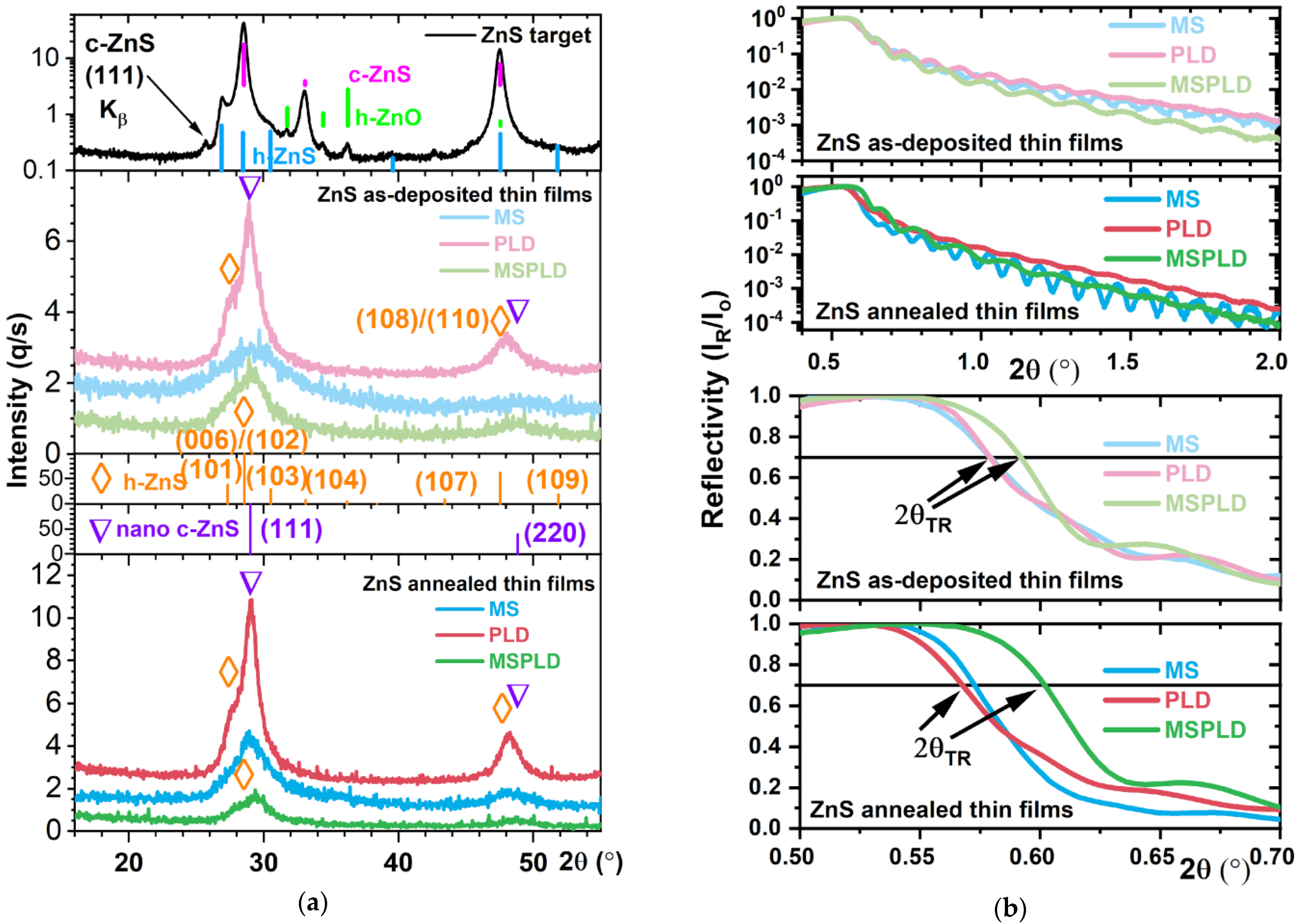
The chemical composition of the ZnS thin films is inferred from the Rutherford backscattering spectrometry (RBS) measurements. The registered parameters, thickness and concentration of each atomic species are presented in Table 1. The composition of the PLD thin film is closest to stoichiometric 50:50, as expected, while, for the others, the Zn-rich nature is slightly enhanced. The MSPLD films are the poorest in sulphur and the thinnest samples. Laser pulses increase the sulphur loss during deposition. Thickness measurements from RBS are given in thin film units (TFU), where 1 TFU = 1015 atoms/cm.

3.2. XRD Analysis

The grazing incidence X-ray diffraction (GIXRD) patterns of the three types of ZnS thin films, in the as-deposited state and after annealing at 400 °C, are shown in Figure 1a. Although annealing at higher temperatures would favor obtaining single-phase films, a lower annealing temperature was chosen, of 400 °C, because it allows for detecting the degree of metastability of the as-deposited samples, thus revealing the performance of each deposition method, and a better understanding of ZnS polymorphism. In addition, a higher annealing temperature might change the stoichiometry dramatically [24,41], or produce an increased micro-strain and dislocation density [42]. Moreover, reactions with the residual oxygen take place above 400 °C leading to unwanted ZnO phases and/or detrimental high surface roughness [43].
The atomic structure of the samples is summarized in Table 2. The ratio of each phase (amorphous, nanocrystalline c-ZnS, or nanocrystalline h-ZnS), denoted in general as phase j, is determined from the X-ray diffractograms as follows: (i) the X-ray background is subtracted from each diffractogram; (ii) the total area (Atotal) of the diffractogram is calculated; (iii) the overlapping crystalline peaks are separated by deconvolution, using a Lorentz profile (in the case of as-deposited MSPLD, the amorphous ZnS peak, taken from the as-deposited MS sample and multiplied by a suitable subunit factor, is subtracted before the deconvolution); (iv) the total area (Aj) of the peaks of each phase is computed; (v) the ratio of phase j is the ratio Aj/Atotal. The average crystallites size is computed from the line broadening (β), where β is the ratio between the peak area and peak amplitude after subtracting the instrumental line broadening, of the (111) (c-ZnS) and (101) (h-ZnS) peaks, using the Scherrer equation. For comparison, the ZnS target, used to produce the ZnS thin films with the three methods, was also characterized. The target consists of 95% polycrystalline cubic ZnS (lattice constant a = 5.406 Å, ICDD file # 00-005-0566, F-43m (216) space group), 4% polycrystalline hexagonal ZnS (ICDD file # 00-036-1450, P63mc (186) space group), and traces (1%) of hexagonal ZnO.
The as-deposited MS samples are fully amorphous, the PLD thin films are nanocrystalline (55% c-ZnS and 45% h-ZnS), while the MSPLD thin films are a mixture of amorphous (57%) and nanocrystalline phases (25% c-ZnS and 18% h-ZnS). The signature of the amorphous ZnS phase in the GIXRD pattern of the as-deposited MS samples is the very large peak at 29.28° (FWHM is 6.5° compared to 3.0° after annealing), and the higher background, because X-rays are scattered rather than diffracted, as compared to the annealed MS samples. Therefore, there are large differences between the structural order in the as-deposited MS and PLD thin films, while the as-deposited MSPLD thin films show a combination between the two. Because the MSPLD method implies the simultaneous deposition from the same target by MS and PLD, it can be inferred, from the MS and PLD deposition parameters, that MS mainly sputters atoms from the surface of the target and, at the condensation on the cold substrate, they form a disordered network with compositional disorder, while PLD mainly ablates droplets which condensate on the substrate and form nanocrystallites because the compositional order is maintained.
After annealing, all the samples are fully crystalline. The thin films obtained by MS crystallize in a single nano-phase, the polycrystalline c-ZnS, with the average crystallite size of 2 nm. Moss et al. [44] showed that the minimum diameter of a “spherical” silicon cluster has a crystalline structure is 1.2 nm. Whereas the length of Zn-S and Si-Si bonds are similar (0.241 vs. 0.235 nm) and the silicon atoms are also tetrahedrally coordinated as zinc and sulfur atoms in ZnS, this means that, indeed, the ZnS clusters with an average size of only 2 nm are crystalline. Similar values were obtained by Włodarski et al. [41]. The same nano-phase becomes dominant (73%) in the annealed PLD samples, leading to the conclusion that c-ZnS is favored at 400 °C. No significant changes are observed in the ratio between the amount of c-ZnS and that of h-ZnS for the annealed MSPLD samples, which means that the transformation of the amorphous phase occurs by growing the size of the existing crystalline seeds (in as-deposited state), instead of producing new crystallization centers. The average crystallite size of all the samples is below 10 nm.
The nanometric cubic ZnS phase, found in the as-deposited PLD and MSPLD films as well as in all the annealed samples, has a smaller lattice constant (a = 5.3 Å, ICDD file # 00-065-0722) than that of the cubic phase present in the target, which means that, in all mentioned samples, there are vacancies in high concentration and the annealing temperature is too low to allow massive network reorganization and the growth of average crystallite size.
From the X-ray reflectometry diagrams (Figure 1b), of the three types of ZnS thin films, the position of the X-rays’ total reflection (TR) edge (2θTR) was calculated, defined as the 2θ angle where the reflectivity (i.e., the intensity of the reflected X-ray at divided by the maximum intensity of the reflected X-ray) decreases by 30% of the maximum. The average thickness (hmean) of the thin films is computed as λ/2θmean, where λ is the X-rays Kα wavelength, and 2θmean is the average period of interference fringes. The results are given in Table 3. The highest value of the average mass density (ρm ~ 2θTR, which allows us to determine the relative variation of mass density without knowing its absolute value) is obtained for the MSPLD thin films, both in the as-deposited state and after annealing. Considering that PLD is a punctual technique and the lateral thickness profiles are sharply falling [45,46] compared with the thickness variations of MS [47], the thickness difference can be explained this way. The highest value of the average mass density (ρm ~ 2θTR, which allows us to determine the relative variation of mass density without knowing its absolute value) is obtained for the MSPLD thin films, both in the as-deposited state and after annealing. Moreover, only the ρm of the MSPLD film increases after annealing with +3.4% due to the decrease of the voids between crystallites, new ZnS crystallites are not formed, only their average size increases. The mass density of the MS and PLD thin films decreases after annealing (with −2.1% and −3.8%, respectively). For the PLD and MSPLD samples, the thickness variation after annealing corresponds to the variation of ρm. In the case of MS samples, the thickness is unchanged, although the density decreases with −2.1%, which may be due to sulfur evaporation. For the PLD thin films, the decrease of ρm with −3.8% after annealing is due to the increase of the voids between crystallites. New ZnS crystallites are formed (the area of crystalline peaks increases with +5.9%), which produces an effect even stronger than the decrease of the voids due to the increase of average crystallite size. However, the average mass density inferred from XRR is the value for clusters plus the voids between clusters. A more precise value could be computed from XRD using a model for the unit cell.

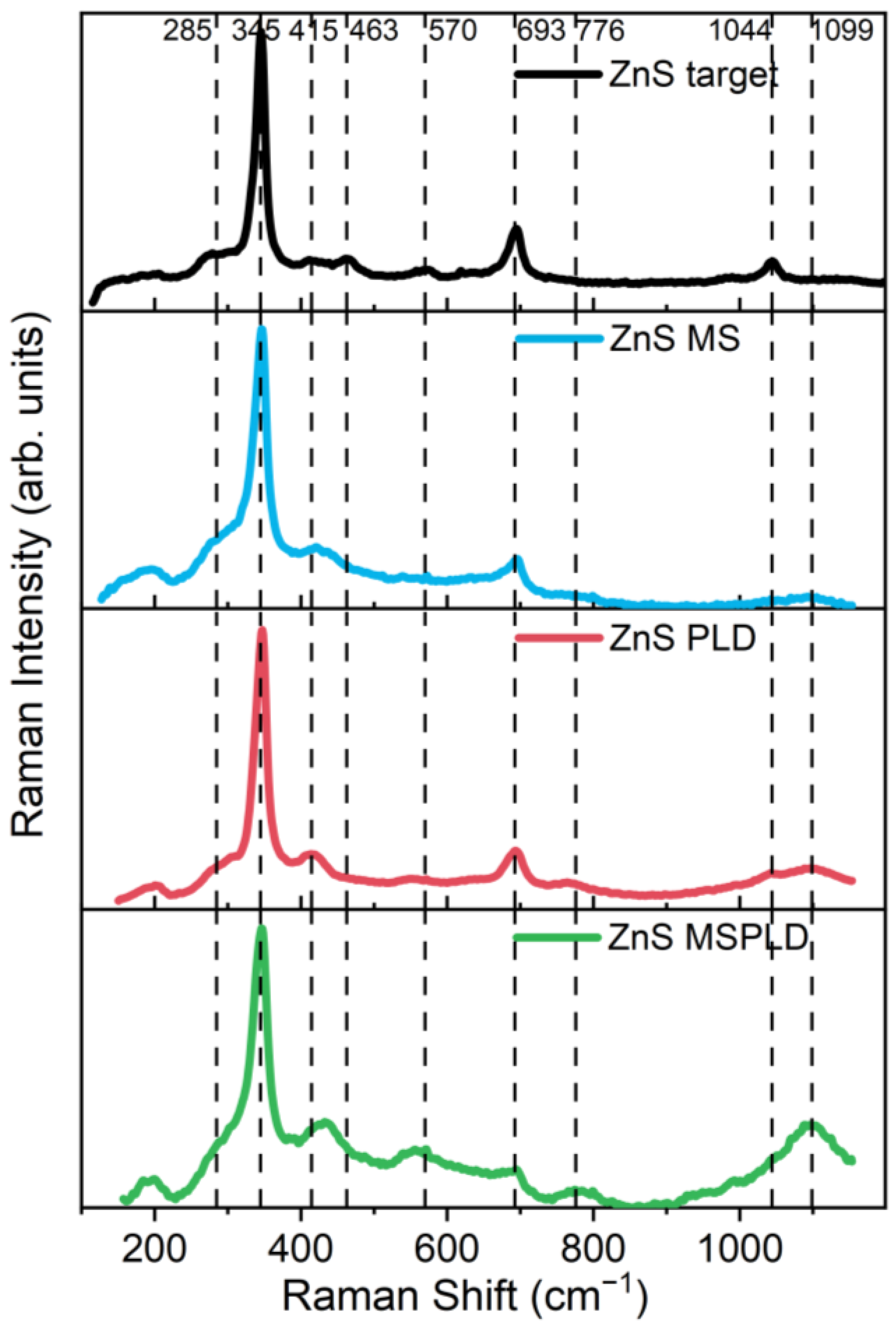
3.3. Raman Spectroscopy

Figure 2 shows the Raman spectra obtained with UV excitation (λ = 325 nm) on the glass deposited films, after the heat treatment. For comparison, the Raman spectrum of the ZnS target is also presented. It is observed that the most intense maximum at 345 cm−1, is not shifted in the case of thin films, compared to the target, suggesting that the predominant c-ZnS phase is preserved. Some additional peaks are observed in the range 400–800 cm−1 (415, 463, 570, 693 and 776 cm−1) that are due to the second order Raman scattering, while the peak at 1090 cm−1 is a combination of third order Raman scattering and luminescence [48,49,50].
Even though the first papers that studied the first and second Raman modes on wurtzite and zinc-blende ZnS have been published since 1969 [51,52,53,54,55,56,57], there are still controversies regarding the correct assignment of the phonon modes involved for both structures. Assignments of the modes in the literature are summarized in Table 4. The LA mode for cubic ZnS, in Table 4, estimated by Nilsen [53] at the X point in the Brillouin Zone, was 110 cm−1, which is far lower than the experimental value (210 cm−1) obtained by neutron scattering [52]. Xiong et al. [57] observed another mode at 335 cm−1 in the study of wurtzite ZnS nanowires, and they assigned it to the surface optical (SO) mode.
Note that, for the second order as well as for the first order Raman features, the shifts also depend on the symmetry line or symmetry point in the Brillouin Zone. For the values presented in Table 4, we have chosen those that are close to the values that we have obtained. According to Table 4, the maximum at 345 cm−1 can be attributed to both c-ZnS and h-ZnS phases [53,54]; however, since the MS film contains a single zinc blende phase, it can be inferred that it belongs to the cubic phase. Moreover, the peak at 776 cm−1 has the highest intensity in the MSPLD sample. This peak together with the shift in the maximum at 415 cm−1 can be an important hint for the identification of h-ZnS.

3.4. Spectroscopic Ellipsometry and Tranmission Spectroscopy

The spectroscopic ellipsometry spectra of zinc sulfide have been modeled, in the spectral range 500–950 nm, using a Cauchy dispersion law. In this spectral region, the extinction coefficient is zero. The thickness of the film and the value of the refractive index at 633 nm are presented in Table 5.
From Table 5, after annealing, in the films deposited on silicon substrate, a small contraction of the MSPLD structures is noticed. Therefore, the density of the thin films becomes significantly higher and the refractive index will increase slightly. It should be noted that the refractive index can be used as a qualitative indicator of film mass density. This is confirmed by the agreement of the results with the XRR measurements. The refractive indices of as-deposited MS, PLD, and MSPLD, which are between 2.30 and 2.33, are similar to the ones found in literature [58,59]. ZnS is a very well-known high-index material for VIS–MIR applications. The increase of the refractive index for all three methods after annealing might indicate a densification of the material.
Additional transmittance measurements of the as-deposited and annealed ZnS thin films on glass substrates were made. The band gap values can be estimated by extrapolating the straight-line segment in the graph of (αhυ)1/2 versus hυ, as shown in Figure 3. The estimated optical band gap ranges from 3.32 to 3.63 eV. The small variation can be associated with the deposition method. Annealing produces a small increase of the band gap, which is expected, since the crystalline phase has a larger fill fraction. On the other hand, the crystallites are extremely small (less than 10 nm) and the disordered phase (including grain boundaries) still dictates the optical band gap.
The band gap values obtained for the films are slightly smaller than the expected band gaps for bulk ZnS (Eg = 3.6 eV [60]) and h-ZnS films (Eg = 3.91 eV), but comparable to polycrystalline c-ZnS films (Eg between 3.29 and 3.79) [61,62,63,64]. Moreover, the as-deposited MS film has a band gap close to the reported value of the amorphous ZnS films (Eg = 3.4 eV) [65]. In addition to the variation produced by the deposition method, the sulphur vacancies, which were confirmed by XRR and RBS measurements, might contribute to the decrease of the bandgap [66].

4. Conclusions

The influence of the deposition method and annealing process on the compositional, structural, and optical properties of ZnS thin films have been investigated. MSPLD offers a higher deposition rate compared with MS and PLD alone. All the films are Zn-rich and the composition of the films obtained by PLD is much closer to the stoichiometric composition with only 2.3% sulphur deficiency, compared to MS and MSPLD. In terms of mass density, the MSPLD films are the densest and the density increased after annealing by +3.4% due to the decrease of the voids between crystallites as a consequence of crystallite growth.
Regarding ZnS polymorphism, the as-deposited MS films are fully amorphous, which is remarkable for this material because it crystallizes very easily, and then undergoes a transition to a single cubic nanocrystalline phase after annealing. On the other hand, the as-deposited PLD and MSPLD films are a mixture of two nanocrystalline c-ZnS and h-ZnS phases. Remarkably, after annealing, the c-ZnS increases for the PLD films since it is favored at 400 °C, and is almost unchanged in the MSPLD layers. An intense maximum at 345 cm−1 was identified in all the films, which can be clearly attributed to the c-ZnS phase.
The band gap is between 3.3 and 3.6 eV in all the films and is not significantly affected by the thermal treatment, which is desirable in photovoltaic structures since changes can detrimentally alter the material properties. Moreover, the possibility to control the composition of the ZnS film and thus its optical properties is an advantage of the MSPLD technique.
In conclusion, for solar cells, either of the three deposition methods can be selected to tune the bandgap. However, MS is more suitable to obtain single phase crystalline films, whereas PLD leads to films with the least S vacancies. MSPLD films are the most stable for annealing treatments with regard to maintaining the c-ZnS to h-ZnS ratio.

Author Contributions

Conceptualization, A.-C.G., C.M. and A.V.; methodology, A.-C.G. and A.V.; formal analysis, I.-D.S., F.S., A.-T.B., A.-C.G., I.B., N.B. and A.V.; investigation, F.S., A.-T.B., I.-D.S., I.B., N.B. and A.-C.G.; resources, A.V.; writing—original draft preparation, I.-D.S., F.S., A.-T.B., A.-C.G., C.M. and A.V.; writing—review and editing, I.-D.S., F.S., A.-T.B., A.-C.G., C.M. and A.V.; supervision, A.-C.G. and A.V.; project administration, A.V.; funding acquisition, A.V. All authors have read and agreed to the published version of the manuscript.

Funding

This work was supported by the Romanian Ministry of Research and Innovation in the framework of the POC-G 54/2016 MAT2IT (contract No. 1550/2018) and Core Program PN19-03 (contract No. 21 N/08.02.2019) projects.

Institutional Review Board Statement

Not applicable.

Informed Consent Statement

Not applicable.

Data Availability Statement

The data presented in this study are available on a reasonable request from the corresponding author.

Acknowledgments

Ion beam experiments have been performed at the 3 MV Tandetron accelerator from “Horia Hulubei” National Institute for Physics and Nuclear Engineering (IFIN-HH) and were supported by the Romanian Governmental Program through the National Program “Instalații și Obiective de Interes Național”.

Conflicts of Interest

The authors declare no conflict of interests.

References

  1. Kwon, B.-H.; Lee, K.G.; Park, T.J.; Kim, H.; Lee, T.J.; Lee, S.J.; Jeon, D.Y. Continuous in situ synthesis of ZnSe/ZnS core/shell quantum dots in a microfluidic reaction system and its application for light-emitting diodes. Small 2012, 8, 3257–3262. [Google Scholar] [CrossRef] [PubMed]
  2. Ippen, C.; Greco, T.; Kim, Y.; Kim, J.; Oh, M.S.; Han, C.J.; Wedel, A. ZnSe/ZnS quantum dots as emitting material in blue QD-LEDs with narrow emission peak and wavelength tunability. Org. Electron. 2014, 15, 126–131. [Google Scholar] [CrossRef]
  3. Ye, X.; Li, Y.; Dong, J.; Xiao, J.; Ma, Y.; Qi, L. Facile synthesis of ZnS nanobowl arrays and their applications as 2D photonic crystal sensors. J. Mater. Chem. C 2013, 1, 6112. [Google Scholar] [CrossRef]
  4. Lemarquis, F.; Marchand, G.; Amra, C. Design and manufacture of low-absorption ZnS–YF3 antireflection coatings in the 3.5–16-μm spectral range. Appl. Opt. 1998, 37, 4239–4244. [Google Scholar] [CrossRef]
  5. Turgut, G.; Keskenler, E.F.; Aydın, S.; Doğan, S.; Duman, S.; Sonmez, E.; Esen, B.; Düzgün, B. A study on characterization of Al/ZnS/p-Si/Al heterojunction diode synthesized by sol–gel technique. Mater. Lett. 2013, 102–103, 106–108. [Google Scholar] [CrossRef]
  6. Toma, O.; Ion, L.; Iftimie, S.; Antohe, V.; Radu, A.; Raduta, A.; Manica, D.; Antohe, S. Physical properties of rf-sputtered ZnS and ZnSe thin films used for double-heterojunction ZnS/ZnSe/CdTe photovoltaic structures. Appl. Surf. Sci. 2019, 478, 831–839. [Google Scholar] [CrossRef]
  7. Mann, J.; Li, J.; Repins, I.; Ramanathan, K.; Glynn, S.; Dehart, C.; Noufi, R. Reflection optimization for alternative thin-film photovoltaics. IEEE J. Photovolt. 2012, 3, 472–475. [Google Scholar] [CrossRef]
  8. Haldar, S.K. Hazards of minerals—rocks and sustainable development. In Introduction to Mineralogy and Petrology; Elsevier: Amsterdam, The Netherlands, 2020; pp. 377–410. ISBN 9780128205853. [Google Scholar]
  9. Gupta, A. Materials: Abundance, Purification, and the Energy Cost Associated with the Manufacture of Si, CdTe, and CIGS PV. In A Comprehensive Guide to Solar Energy Systems; Elsevier: Amsterdam, The Netherlands, 2018; pp. 445–467. ISBN 9780128114797. [Google Scholar] [CrossRef]
  10. Scott, S.; Barnes, H. Sphalerite-wurtzite equilibria and stoichiometry. Geochim. Cosmochim. Acta 1972, 36, 1275–1295. [Google Scholar] [CrossRef]
  11. Rickard, D. Aqueous Metal–Sulfide Chemistry. In Developments in Sedimentology; Elsevier: Amsterdam, The Netherlands, 2012; Volume 65, pp. 121–194. ISBN 9780444529893. [Google Scholar] [CrossRef]
  12. Barreca, D.; Gasparotto, A.; Maragno, C.; Tondello, E. CVD of Nanosized ZnS and CdS Thin Films from Single-Source Precursors. J. Electrochem. Soc. 2004, 151, G428. [Google Scholar] [CrossRef]
  13. Chu, T.L.; Chu, S.S. Thin film II–VI photovoltaics. Solid-State Electron. 1995, 38, 533–549. [Google Scholar] [CrossRef]
  14. Nguyen, M.; Ernits, K.; Tai, K.F.; Ng, C.F.; Pramana, S.; Sasangka, W.A.; Batabyal, S.K.; Holopainen, T.; Meissner, D.; Neisser, A.; et al. ZnS buffer layer for Cu2ZnSn(SSe)4 monograin layer solar cell. Sol. Energy 2014, 111, 344–349. [Google Scholar] [CrossRef]
  15. Moore, D.; Wang, Z.L. Growth of anisotropic one-dimensional ZnS nanostructures. J. Mater. Chem. 2006, 16, 3898–3905. [Google Scholar] [CrossRef]
  16. Housecroft, C.E.; Sharpe, A.G. Inorganic Chemistry, 3rd ed.; Pearson Education: Harlow, UK, 2008. [Google Scholar]
  17. Goswami, A. Dielectric and optical properties of ZnS films. Thin Solid Films 1973, 16, 175–185. [Google Scholar] [CrossRef]
  18. Pässler, R.; Griebl, E.; Riepl, H.; Lautner, G.; Bauer, S.; Preis, H.; Gebhardt, W.; Buda, B.; As, D.J.; Schikora, D.; et al. Temperature dependence of exciton peak energies in ZnS, ZnSe, and ZnTe epitaxial films. J. Appl. Phys. 1999, 86, 4403–4411. [Google Scholar] [CrossRef] [Green Version]
  19. Islam, M.M.; Ishizuka, S.; Yamada, A.; Sakurai, K.; Niki, S.; Akimoto, K. CIGS solar cell with MBE-grown ZnS buffer layer. Sol. Energy Mater. Sol. Cells 2009, 93, 970–972. [Google Scholar] [CrossRef]
  20. Kavanagh, Y.; Cameron, D. Zinc sulfide thin films produced by sulfidation of sol–gel deposited zinc oxide. Thin Solid Films 2001, 398–399, 24–28. [Google Scholar] [CrossRef]
  21. Arenas, O.L.; Nair, M.T.S.; Nair, P.K. Chemical bath deposition of ZnS thin films and modification by air annealing. Semicond. Sci. Technol. 1997, 12, 1323–1330. [Google Scholar] [CrossRef]
  22. Murali, K.; Vasantha, S.; Rajamma, K. Properties of pulse plated ZnS films. Mater. Lett. 2008, 62, 1823–1826. [Google Scholar] [CrossRef]
  23. Yano, S.; Schroeder, R.; Ullrich, B.; Sakai, H. Absorption and photocurrent properties of thin ZnS films formed by pulsed-laser deposition on quartz. Thin Solid Films 2003, 423, 273–276. [Google Scholar] [CrossRef]
  24. Hwang, D.H.; Ahn, J.H.; Hui, K.N.; Hui, K.S.; Son, Y.G. Structural and optical properties of ZnS thin films deposited by RF magnetron sputtering. Nanoscale Res. Lett. 2012, 7, 26. [Google Scholar] [CrossRef] [Green Version]
  25. Lee, E.Y.M.; Tran, N.H.; Russell, J.J.; Lamb, R.N. Structure Evolution in Chemical Vapor-Deposited ZnS Films. J. Phys. Chem. B 2003, 107, 5208–5211. [Google Scholar] [CrossRef]
  26. Marszalek, K.W. Large area deposition sputtering coaters. In Vacuum Technique & Technology; Monographs of Tele & Radio Research Institute: Warsaw, Poland, 2014; pp. 44–54. [Google Scholar] [CrossRef]
  27. Ekpe, S.D.; Jiménez, F.J.; Field, D.J.; Davis, M.J.; Dew, S.K. Effect of magnetic field strength on deposition rate and energy flux in a dc magnetron sputtering system. J. Vac. Sci. Technol. A 2009, 27, 1275. [Google Scholar] [CrossRef]
  28. Kelly, P.; Arnell, R. Magnetron sputtering: A review of recent developments and applications. Vacuum 2000, 56, 159–172. [Google Scholar] [CrossRef]
  29. Willmott, P.R.; Huber, J.R. Pulsed laser vaporization and deposition. Rev. Mod. Phys. 2000, 72, 315–328. [Google Scholar] [CrossRef]
  30. Schou, J. Physical aspects of the pulsed laser deposition technique: The stoichiometric transfer of material from target to film. Appl. Surf. Sci. 2009, 255, 5191–5198. [Google Scholar] [CrossRef]
  31. Bimashofer, G.; Smetaczek, S.; Gilardi, E.; Schneider, C.W.; Limbeck, A.; Lippert, T.; Stahn, J. Growth of LixLaySrzMnO3 thin films by pulsed laser deposition: Complex relation between thin film composition and deposition parameters. Appl. Phys. A 2021, 127, 1–8. [Google Scholar] [CrossRef]
  32. Verardi, P.; Craciun, F.; Mirenghi, L.; Dinescu, M.; Sandu, V. An XPS and XRD study of physical and chemical homogeneity of Pb(Zr,Ti)O3 thin films obtained by pulsed laser deposition. Appl. Surf. Sci. 1999, 138–139, 552–556. [Google Scholar] [CrossRef]
  33. Andreić, Z.; Aschke, L.; Kunze, H.-J. The presence of droplets in pulsed laser deposition of aluminum with capillary ablation targets. Appl. Surf. Sci. 2000, 153, 235–239. [Google Scholar] [CrossRef]
  34. Yoshitake, T.; Shiraishi, G.; Nagayama, K. Elimination of droplets using a vane velocity filter for pulsed laser ablation of FeSi2. Appl. Surf. Sci. 2002, 197-198, 379–383. [Google Scholar] [CrossRef]
  35. Voevodin, A.A.; Capano, M.A.; Safriet, A.J.; Donley, M.S.; Zabinski, J.S. Combined magnetron sputtering and pulsed laser deposition of carbides and diamond-like carbon films. Appl. Phys. Lett. 1996, 69, 188–190. [Google Scholar] [CrossRef]
  36. Benetti, D.; Nouar, R.; Nechache, R.; Pepin, H.; Sarkissian, A.; Rosei, F.; MacLeod, J.M. Combined magnetron sputtering and pulsed laser deposition of TiO2 and BFCO thin films. Sci. Rep. 2017, 7, 1–9. [Google Scholar] [CrossRef] [Green Version]
  37. Simandan, I.-D.; Sava, F.; Buruiana, A.-T.; Galca, A.-C.; Becherescu, N.; Burducea, I.; Mihai, C.; Velea, A. Influence of deposition method on the structural and optical properties of Ge2Sb2Te5. Materials 2021, 14, 3663. [Google Scholar] [CrossRef]
  38. Chrzanowska-Giżyńska, J.; Denis, P.; Giżyński, M.; Kurpaska, L.; Mihailescu, I.; Ristoscu, C.; Szymański, Z.; Mościcki, T. Thin WBx and WyTi1−yBx films deposited by combined magnetron sputtering and pulsed laser deposition technique. Appl. Surf. Sci. 2019, 478, 505–513. [Google Scholar] [CrossRef]
  39. Burducea, I.; Straticiuc, M.; Ghiță, D.; Moșu, D.; Călinescu, C.; Podaru, N.; Mous, D.; Ursu, I.; Zamfir, N. A new ion beam facility based on a 3 MV Tandetron™ at IFIN-HH, Romania. Nucl. Instrum. Methods Phys. Res. Sect. B Beam Interact. Mater. Atoms 2015, 359, 12–19. [Google Scholar] [CrossRef]
  40. Mayer, M. SIMNRA User’s Guide Technical Report IPP 9/133, MPI für Plasmaphysik, Garching, Germany 1997. Available online: https://www2.ipp.mpg.de/~mam/ (accessed on 2 September 2021).
  41. Włodarski, M.; Chodorow, U.; Jóźwiak, S.; Putkonen, M.; Durejko, T.; Sajavaara, T.; Norek, M. Structural and optical characterization of ZnS ultrathin films prepared by low-temperature ALD from diethylzinc and 1.5-pentanedithiol after various annealing treatments. Materials 2019, 12, 3212. [Google Scholar] [CrossRef] [Green Version]
  42. Bashar, M.S.; Matin, R.; Sultana, M.; Siddika, A.; Rahaman, M.; Gafur, M.A.; Ahmed, F. Effect of rapid thermal annealing on structural and optical properties of ZnS thin films fabricated by RF magnetron sputtering technique. J. Theor. Appl. Phys. 2019, 14, 53–63. [Google Scholar] [CrossRef] [Green Version]
  43. Mohamed, S.; El-Hagary, M.; Emam-Ismail, M. Thickness and annealing effects on the optoelectronic properties of ZnS films. J. Phys. D: Appl. Phys. 2010, 43, 075401. [Google Scholar] [CrossRef]
  44. Moss, S.C.; Graczyk, J.F. Evidence of voids within the as-deposited structure of glassy silicon. Phys. Rev. Lett. 1969, 23, 1167–1171. [Google Scholar] [CrossRef]
  45. Axente, E.; Socol, G.; Beldjilali, S.A.; Mercadier, L.; Luculescu, C.R.; Trinca, L.; Galca, A.C.; Pantelica, D.; Ionescu, P.; Becherescu, N.; et al. Quantitative analysis of amorphous indium zinc oxide thin films synthesized by combinatorial pulsed laser deposition. Appl. Phys. A 2014, 117, 229–236. [Google Scholar] [CrossRef]
  46. Craciun, D.; Socol, G.; Axente, E.; Galca, A.-C.; Singh, R.; Craciun, V. Microstructural investigations of hafnium aluminum oxide films. MRS Proc. 2008, 1074, 1074-I03-18. [Google Scholar] [CrossRef]
  47. Tite, T.; Popa, A.; Chirica, I.; Stuart, B.; Galca, A.; Balescu, L.; Popescu-Pelin, G.; Grant, D.; Ferreira, J.; Stan, G. Phosphate bioglass thin-films: Cross-area uniformity, structure and biological performance tailored by the simple modification of magnetron sputtering gas pressure. Appl. Surf. Sci. 2020, 541, 148640. [Google Scholar] [CrossRef]
  48. Scott, J.; Damen, T.; Silfvast, W.; Leite, R.; Cheesman, L. Resonant raman scattering in ZnS and ZnSe with the cadmium laser. Opt. Commun. 1970, 1, 397–399. [Google Scholar] [CrossRef]
  49. Nilsen, W.G. Second-Order Raman Spectra of Some Zinc Blende and Wurtzite Crystals. In Light Scattering Spectra of Solids; Wright, G.B., Ed.; Springer: Berlin/Heidelberg, Germany, 1969; pp. 129–137. ISBN 9783642873591. [Google Scholar] [CrossRef]
  50. La Porta, F.A.; Andrés, J.; Li, M.S.; Sambrano, J.R.; Varela, J.A.; Longo, E. Zinc blende versus wurtzite ZnS nanoparticles: Control of the phase and optical properties by tetrabutylammonium hydroxide. Phys. Chem. Chem. Phys. 2014, 16, 20127–20137. [Google Scholar] [CrossRef]
  51. Cheng, Y.; Jin, C.; Gao, F.; Wu, X.; Zhong, W.; Li, S.; Chu, P. Raman scattering study of zinc blende and wurtzite ZnS. J. Appl. Phys. 2009, 106, 123505. [Google Scholar] [CrossRef]
  52. Vagelatos, N. Phonon dispersion and phonon densities of states for ZnS and ZnTe. J. Chem. Phys. 1974, 60, 3613–3618. [Google Scholar] [CrossRef] [Green Version]
  53. Nilsen, W.G. Raman spectrum of cubic ZnS. Phys. Rev. 1969, 182, 838–850. [Google Scholar] [CrossRef]
  54. Brafman, O.; Mitra, S.S. Raman effect in wurtzite- and Zinc-blende-type ZnS single crystals. Phys. Rev. 1968, 171, 931–934. [Google Scholar] [CrossRef]
  55. Schneider, J.; Kirby, R.D. Raman scattering from ZnS polytypes. Phys. Rev. B 1972, 6, 1290–1294. [Google Scholar] [CrossRef] [Green Version]
  56. Serrano, J.; Cantarero, A.; Cardona, M.; Garro, N.; Lauck, R.; Tallman, R.E.; Ritter, T.M.; Weinstein, B.A. Raman scattering in β-ZnS. Phys. Rev. B 2004, 69, 014301. [Google Scholar] [CrossRef]
  57. Xiong, Q.; Wang, J.; Reese, O.; Voon, L.C.L.Y.; Eklund, P.C. Raman scattering from surface phonons in rectangular cross-sectional w-ZnS nanowires. Nano Lett. 2004, 4, 1991–1996. [Google Scholar] [CrossRef]
  58. Debenham, M. Refractive indices of zinc sulfide in the 0.405–13-μm wavelength range. Appl. Opt. 1984, 23, 2238–2239. [Google Scholar] [CrossRef]
  59. Amotchkina, T.; Trubetskov, M.; Hahner, D.; Pervak, V. Characterization of e-beam evaporated Ge, YbF3, ZnS, and LaF3 thin films for laser-oriented coatings. Appl. Opt. 2019, 59, A40–A47. [Google Scholar] [CrossRef] [PubMed]
  60. Rodríguez, C.; Sandoval-Paz, M.; Cabello, G.; Flores, M.; Fernández, H.; Carrasco, C. Characterization of ZnS thin films synthesized through a non-toxic precursors chemical bath. Mater. Res. Bull. 2014, 60, 313–321. [Google Scholar] [CrossRef]
  61. Tran, T.K.; Park, W.; Tong, W.; Kyi, M.M.; Wagner, B.K.; Summers, C.J. Photoluminescence properties of ZnS epilayers. J. Appl. Phys. 1997, 81, 2803–2809. [Google Scholar] [CrossRef]
  62. Kanehisa, O.; Shiiki, M.; Migita, M.; Yamamoto, H. Luminescence properties of ZnS/GaAs grown by gas source MBE. J. Cryst. Growth 1988, 86, 367–371. [Google Scholar] [CrossRef]
  63. Doña, J.M.; Herrero, J. Process and film characterization of chemical-bath-deposited ZnS thin films. J. Electrochem. Soc. 1994, 141, 205–210. [Google Scholar] [CrossRef]
  64. Vall, C.M.S.; Chaik, M.; Dads, H.A.; El Aakib, H.; Elyaagoubi, M.; Aggour, M.; Outzourhit, A. Effect of RF power on the structural and optical properties of ZnS thin films prepared by RF-sputtering. J. Semicond. 2018, 39, 123001. [Google Scholar] [CrossRef]
  65. Maruyama, T.; Kawaguchi, T. ZnS thin films prepared by thermal decomposition of a coordination compound. Thin Solid Films 1990, 188, 323–327. [Google Scholar] [CrossRef]
  66. Wang, G.; Huang, B.; Li, Z.; Lou, Z.; Wang, Z.; Dai, Y.; Whangbo, M.-H. Synthesis and characterization of ZnS with controlled amount of S vacancies for photocatalytic H2 production under visible light. Sci. Rep. 2015, 5, 8544. [Google Scholar] [CrossRef]
Figure 1. Grazing incidence X-ray diffraction patterns (a) and X-ray reflectivity diagrams (b) for the ZnS thin films obtained by MS, PLD, and MSPLD, in the as-deposited state and annealed at 400 °C. Additionally, the GIXRD diagram of the ZnS target and the ICDD files # 00-005-0566 (cubic ZnS, F-43m (216) space group), # 00-036-1450 (hexagonal ZnS, P63mc (186) space group) and # 04-003-2106 (hexagonal ZnO, P63mc (186) space group) are presented. The positions of the total reflection edge (2θTR), defined as the angle where the reflectivity decreases by 30% of the maximum, are indicated. The GIXRD patterns are displaced vertically for a better representation.
Coatings 11 01064 g001
Figure 2. Raman spectra, at λ = 325 nm laser excitation, of the ZnS samples deposited by MS, PLD, and MSPLD, after annealing. The spectrum for the ZnS target is shown for comparison.
Coatings 11 01064 g002
Figure 3. Tauc plots of ZnS films deposited on glass, by all three methods, in the (a) as deposited and (b) annealed states.
Coatings 11 01064 g003
Table 1. RBS composition of the ZnS thin films.
Deposition MethodThickness (TFU)Composition (at. %)
ZnS
MS49554.745.3
PLD35352.347.7
MSPLD22455.344.7
Table 2. The crystalline phases in the three types of ZnS thin films. The average size of the crystallites was approximated using Scherrer equation for the (111) c-ZnS peak.
As-DepositedAnnealed at 400 °C
MS
  • 100% amorphous
  • 100% Nanocrystalline cubic ZnS, space group F-43m (216), ICDD file # 00-065-0722. (the average size of the crystallites is 2 nm)
PLD
  • (55%) Nanocrystalline cubic ZnS, space group F-43m (216), ICDD file # 00-065-0722. (the average size of the crystallites is 8 nm)
  • (45%) Nanocrystalline hexagonal ZnS, space group P63mc (186), ICDD file 01-089-2191.
  • (73%) Nanocrystalline cubic ZnS, space group F-43m (216), ICDD file # 00-065-0722. (the average size of the crystallites is 10 nm)
  • (27%) Nanocrystalline hexagonal ZnS, space group P63mc (186), ICDD file 01-089-2191.
MSPLD
  • (57%) amorphous
  • (25%) Nanocrystalline cubic ZnS, space group F-43m (216), ICDD file # 00-065-0722. (the average size of the crystallites is 3 nm)
  • (18%) Nanocrystalline hexagonal ZnS, space group P63mc (186), ICDD file 01-089-2191.
  • (58%) Nanocrystalline cubic ZnS, space group F-43m (216), ICDD file # 00-065-0722. (the average size of the crystallites is 5 nm)
  • (42%) Nanocrystalline hexagonal ZnS, space group P63mc (186), ICDD file 01-089-2191.
Table 3. Positions of the X-ray’s total reflection edge (2θTR) and the average thickness (hmean) of the ZnS thin films.
Deposition
Method
TR; Δρmohmean; Δhm/ho
As-DepositedAnnealedAs-DepositedAnnealed
MS0.579°0.573°; −2.1%105 nm105 nm; 0%
PLD0.579°0.568°; −3.8%80 nm83 nm; +3.8%
MSPLD0.592°0.602°; +3.4%61 nm59 nm; −3.3%
Table 4. Phonon modes assignment for the first and second order Raman spectrum.
ModeZinc Blende Wurtzite
LARaman Shift (cm−1)Raman Shift (cm−1)
222 [49]
210 [52]
219 [51]
TA181 [49]
A1(TO)271 [53]273 [54], 272 [55]
A1(LO)352 [53]351 [54]
E1(TO) 272 [54], 276 [55], 279 [49]
E1(LO) 351 [54], 351 [55], 348 [49]
TO+LA422 [53], 482 [56]
433 [49]
LO+TA433 [49], 449 [56], 419 [56]427 [51]
2TO621 [49], 612 [53], 614 [56], 607 [56]622 [51]
2LO672 [49], 665 [53], 692 [56]698 [51], 676 [51]
Table 5. ZnS films thicknesses and refractive indices determined by spectroscopic ellipsometry analysis. The layer thickness (Thick), layer roughness (Rough), and the total film thickness (Total) are given.
Deposition
Method
Thickness (nm)n @ 630 nm
As-DepositedAnnealedAs-DepositedAnnealed
ThickRoughTotalThickRoughTotal
MS90141047920992.302.36
PLD69271683712.332.34
MSPLD474513710472.332.48
Publisher’s Note: MDPI stays neutral with regard to jurisdictional claims in published maps and institutional affiliations.

