
Organic Thin Films Deposited by Matrix-Assisted Pulsed Laser Evaporation (MAPLE) for Photovoltaic Cell Applications: A Review


1
National Institute of Materials Physics, 405A Atomistilor, 077125 Magurele, Romania
2
National Institute for Lasers, Plasma and Radiation Physics, 409 Atomistilor, 077125 Magurele, Romania
*
Authors to whom correspondence should be addressed.
†
These authors contributed equally.
Coatings 2021, 11(11), 1368; https://doi.org/10.3390/coatings11111368
Submission received: 29 September 2021
/
Revised: 28 October 2021
/
Accepted: 5 November 2021
/
Published: 8 November 2021
(This article belongs to the Collection Pulsed Laser Deposition of Thin Films: Recent Advances and Challenges)
Abstract
:Human society’s demand for energy has increased faster in the last few decades due to the world’s population growth and economy development. Solar power can be a part of a sustainable solution to this world’s energy need, taking into account that the cost of the renewable energy recently dropped owed to the remarkable progress achieved in the solar panels field. Thus, this inexhaustible source of energy can produce cheap and clean energy with a beneficial impact on the climate change. The considerable potential of the organic photovoltaic (OPV) cells was recently emphasized, with efficiencies exceeding 18% being achieved for OPV devices with various architectures. The challenges regarding the improvement in the OPV performance consist of the selection of the adequate raw organic compounds and manufacturing techniques, both strongly influencing the electrical parameters of the fabricated OPV devices. At the laboratory level, the solution-based techniques are used in the preparation of the active films based on polymers, while the vacuum evaporation is usually involved in the deposition of small molecule organic compounds. The major breakthrough in the OPV field was the implementation of the bulk heterojunction concept but the deposition of mixed films from the same solvent is not always possible. Therefore, this review provides a survey on the development attained in the deposition of organic layers based on small molecules compounds, oligomers and polymers using matrix-assisted pulsed laser evaporation (MAPLE)-based deposition techniques (MAPLE, RIR-MAPLE and emulsion-based RIR-MAPLE). An overview of the influence of various experimental parameters involved in these laser deposition methods on the properties of the fabricated layers is given in order to identify, in the forthcoming years, new strategies for enhancing the OPV cells performance.
1. Introduction
Nowadays, global energy consumption has inexorably increased due to population and economic growth, and worldwide energy production remains largely dependent upon fossil fuels (oil, coal and natural gas). However, during the last few decades, the depletion of the fossil fuel-based energy sources and their negative effects on the environment become critical issues of which humanity is more and more aware. Hence, fossil fuels are the principal contributors to global warming and climate change, taking into account that the carbon dioxide emissions resulted from their burning remain trapped in the atmosphere for a long time, leading to a rise in the average temperature of the Earth. Therefore, a gradual transition from the fossil fuel-based energy sources toward renewable sources has been taking place since the last two decades of the 20th century. Renewable energy sources (sun, wind and water) have considerable potential to meet the world’s demand for reliable and affordable electricity. Thus, these inexhaustible sources of energy can produce cheap and clean energy to support new technologies (electric vehicles, greenhouses, green hydrogen, etc.). It has to be highlighted that in the European Union (EU), in the first half of 2020, 38% of the electricity used in the EU was produced by renewable sources (wind, hydropower, solar and biomass), while 37% came from fossil fuels; renewable electricity generation exceeded fossil fuel generation for the first time ever [1]. The limitation of the renewable energy sources and, at the same time, the main challenge for human society, resides only in our ability to harness these energy sources and to turn them into electricity using efficient and cost-effective technologies.
Solar power is considered the key to a clean energy future being one of the most abundant renewable energy sources available. The potential of solar power is huge: the Sun continuously radiates 173,000 terawatts onto the Earth, which is 10,000 times more power than the planet’s population total energy use [2]. Consequently, solar power can play a crucial role in meeting the world’s energy demand. Moreover, this energy can be a part of the solution to the current climate crisis by reducing our dependence on fossil fuels and minimizing the climate changes. People can harness the Sun’s energy in different ways, with the main approach consisting of solar panels that convert solar energy into electricity. Photovoltaic (PV) technology has a negligible environmental footprint, the breakthroughs consisting of making more and more efficient PV cells. The first silicon solar cell was described by Ohl in 1941 [3], while Chapin, Fuller and Pearson at Bell Laboratories obtained the first practical silicon solar cell in 1954 [4]. Currently, the developed PV devices can be classified in four main generations [5,6], the cells being based on (i) both (mono-) and (poly-) crystalline silicon (Si) wafers and on gallium arsenide (GaAs) wafers; (ii) thin films involving amorphous-Si, cadmium telluride (CdTe), copper indium gallium and selenium (CIGS) and cooper zinc tin sulphide (CZTS); (iii) organic and polymeric, dye sensitized, quantum dot or perovskite materials and (iv) composites combining the organic materials (polymers, small molecules) and inorganic nanostructures. It has to be mentioned that several studies emphasized that nature-inspired designs can play a significant role in the development of future photovoltaic cells, the bio-inspired architectures of these systems favoring the enhancement of the power conversion efficiency [7,8,9].
Organic photovoltaic (OPV) technology has rapidly developed in terms of technological advancements due to its unique benefit: solution-processed materials facilitate the covering of a large-area at a low-cost via scalable printing technologies. Thus, soluble organic compounds enable roll-to-roll processing techniques, resulting in low manufacturing costs. In addition, the flexible solar panels are lightweight, offering the possibility to be placed in locations inaccessible to the heavier silicon-based solar panels for turning light into electricity. Furthermore, the wide abundance of organic materials that can be used as building blocks and the ability to apply them on flexible substrates allows a wide range of applications [10]. In this way, OPV technology provides a great opportunity to produce low-cost and lightweight flexible PV cells facilitating the integration of solar technologies in applications that can make our daily life better (wearables and portable electronics, Internet of Things (IoT) devices, indoor applications, buildings facades, windows, urban, naval and space mobility, etc.) [11,12,13,14,15]. Concerning the indoor applications, some studies revealed that the OPV devices can convert indoor lights (white light-emitting diodes, fluorescent lamps and halogen lamps) into electricity, which can further be used for operating low-power consumption indoor electronic devices [16,17].
Over the past half century of exploration, the structure of OPV devices has evolved from a single layer to stacked layers (multilayers) and then to a bulk heterojunction (BHJ) active layer formed by blending donor and acceptor materials. Thus, the first organic cell based on a magnesium phthalocyanine layer was obtained by Kearns [18] in 1958, in the same year the first satellite having solar cells based on single crystal silicon, Vanguard 1, being launched in space [19]. Lately, in 1986, Tang fabricated an OPV cell using copper phthalocyanine and perylenediimide in a donor/acceptor (D/A) configuration with organic thin films disposed as stacked layers [20]. Further, the major step in the development of OPV cells was the implementation of the BHJ concept [21], the donor:acceptor (D:A) components being mixed in solution and deposited as a single film. In comparison with the stacked architecture, the wide interface formed between the organic components in the mixed configuration increased the exciton dissociation probability facilitating the charge transport. If in 1986, Tang reported a power conversion efficiency of about 1%, the continuous development of materials and interface engineering has led to an enhanced efficiency: in 2021, some studies reported a power conversion efficiency exceeding 18% for OPV cells with various architectures [20,22,23,24,25,26].
Usually, the OPV fabrication employed two architectures: a conventional one with the transparent conductive electrode (TCE) working as an anode and the metal as a cathode and an inverted one with the TCE working as a cathode and the metal as an anode [27]. In the last case, the bottom electrode collects the electrons, while the top electrode collects the holes [28]. Although many attempts were made to use oxides such as fluorine-doped tin oxide (FTO), indium-doped zinc oxide (IZO) or aluminum-doped zinc oxide (AZO) [29] as the TCE, indium tin oxide (ITO) remains the most commonly used TCE due to its high optical transparency and reduced electrical resistivity being commercially available both on rigid (glass) and flexible (plastic) substrates [30]. Another key element of the OPV cells is the metallic contact, its selection being made in relation to the device configuration (conventional or inverted). Thus, metals with low work function (ex. aluminum) are adequate for the OPV in a conventional geometry, while metals with a high work function (ex. gold, silver) can be used as the top electrode in the OPV in an inverted geometry [28]. The insertion of some buffer layers as the hole transport layer (HTL) or as the electron transport layer (ETL) can improve the performance and stability of the OPV devices [31,32]. In the OPV cells, different organic or inorganic (especially metal oxides) compounds are involved as the HTL (also known as the electron blocking layer (EBL), anode buffer layer (ABL)) or as the ETL (also known as hole blocking layer (HBL), cathode buffer layer (CBL)). Although the potential of various metal oxides was tested as an HTL (MoO3, NiO, WO3, etc.) [31] or as an ETL (SnO2, Nb2O5, etc.) [28,33], poly(3,4-ethylenedioxythiophene):poly(styrene sulfonate) (PEDOT:PSS) and ZnO or TiO2 remain the most popular HTL and ETL, respectively.
The development of commercially OPV devices requires a successful transition from lab-scale toward large-scale manufacturing, the achievement of this goal being strongly related by key aspects concerning the choice of materials and processing techniques. Thus, designing organic semiconductors with controlled structural, morphological, optical and electronic properties remains a challenge. Usually, in the OPV devices, the active layers are based on organic small molecules, oligomers or polymers (especially on those with a low bandgap). Taking into account that the polymers are the most promising candidates for high-efficiency OPV devices [34], various solution-processed deposition techniques were involved in their deposition [35]. At the lab-scale, spin coating, dip casting, doctor blading, screen printing or ink jet printing are frequently used in the deposition of polymer layers [35]. Although spin coating remains the most used solution-based technique, only a small amount of the solution (2–5%) is deposited on the substrate to form the film, with the majority of the used solution being lost. Furthermore, in the solution-processed paths, solvent-induced conformational defects in the deposited layers that cannot be controlled influence their morphological properties that, in turn, affect their electrical characteristics [36]. Other disadvantages of this approach consist of (i) the difficulty to deposit organic layers on flexible substrates and on nano-patterned structured substrates, (ii) the preparation of multilayer structures and (iii) the use of materials with different solubilities and substrates with different wettabilities [37].
Matrix-Assisted Pulsed Laser Evaporation (MAPLE) can overcome the drawbacks of spin coating (at the lab-scale level) being a laser technique that allows the deposition of organic (multi)layers [38] or hybrid composite layers [39] with tuned properties even on plastic substrates [40]. MAPLE was developed in the late 1990s in a US Naval Research Laboratory to provide a gentler pulsed laser evaporation process for organic compounds (especially polymers) layers in order to preserve their chemical structure during the deposition [41]. MAPLE is an adaptation of pulsed laser deposition (PLD), a technique that allows a stoichiometric transfer, especially of the inorganic compounds from a source consisting of a pressed solid target, which can contain single or composite materials [42]. However, some papers were reported on the deposition by PLD of small organic compounds frequently used in the OPV area, such as zinc phthalocyanine (ZnPc) or pentacene [43,44]. The studies highlighted (i) the influence of the laser fluence (from 10 to 100 mJ/cm2) and repetition rate (50 and 200 Hz) on the properties of the obtained ZnPc film [43] and (ii) the major impact of the laser fluence and the used wavelength on the electrical characteristics of the pentacene films [44]. The ability of this laser technique to deposit thin films based on polymers has been also evaluated [45,46,47]. Hence, addition-type polymers such as poly-tetrafluorethylene (PTFE) [45] and poly-methylmethacrylate (PMMA) [46,47] have been deposited by PLD. In these cases, the polymeric films are obtained via a “depolymerization–monomer ablation–repolymerization” mechanism [47], which limits the application of PLD as a laser deposition technique for polymeric layers. In addition, some attempts have been made to deposit small molecule compounds or polymers by another variant of PLD, Resonant Infrared-PLD (RIR-PLD) [48,49]. In this case, the laser wavelength is tuned to an absorption band characteristic to the material intended to be deposit (pressed target) [48]. Tris(8-hydroxyquinoline) aluminum (Alq3) films were deposited using a 6.67-micrometer wavelength laser working at a 1.5 J/cm2 fluence [48], while poly [2-methoxy-5-(2-ethylhexyloxy)-1,4-phenylenevinylene] (MEH-PPV) layers were obtained by ablation of the pressed target with an 8.3-micrometer wavelength laser working at a 0.5 J/cm2 fluence [49]. However, the infrared investigations revealed that the Alq3 films preserved the vibrational characteristic bands of the raw compound, while the chemical structure of MEH-PPV was altered during the laser deposition. It has to be mentioned that the PLD deposition is usually carried in a vacuum chamber, under high vacuum. Nevertheless, an experimental set-up with a new configuration that can operate in the open air was recently patented [50]. Up to now, some papers already reported on the application of the pulsed laser deposition in open air (at lab-scale level) in the deposition of metals nanostructures based on Au [51] and Ag [52], and metal oxides nanostructures based on ZnO [53,54], TiO2 [54], SnO2 [54], MoO3 [54] and Fe2O3 [55]. Furthermore, a study published in 2020 on the deposition of nanocomposites based on rare earth phosphor nanoparticles and poly (methyl methacrylate) by concurrent multi-beam multi-target pulsed laser deposition in air proves the feasibility and potential of this deposition technique for producing commercial-size thin-film sunlight down-converters for photovoltaic solar power applications [56].
In comparison with PLD and RIR-PLD, the MAPLE process implies a frozen target containing the materials that are intended to be deposited together with an adequate solvent (host matrix) featured by a strong absorption at the laser wavelength used in the deposition [38,57]. Therefore, the solvent must meet the following requirements: (i) to assure a complete or high dissolution of the organic compound (solute), (ii) to be chemically inert relative to the organic compound and (iii) to be volatile, being pumped away after vaporization [58]. Beside the lower laser fluences (typically no more than 500 mJ/cm2) involved in the MAPLE deposition, an adequate concentration of the organic material (usually 1–5% mass concentration) is required in order to assure the transfer of the compound without damaging its chemical structure or functionality [59,60].
Generally, the term MAPLE is used for denoting a UV-MAPLE process involving UV excimer lasers (193 and 248 nm) or the third and fourth harmonic of the Nd:YAG laser (355 and 266 nm). In this case, the laser photons are preponderantly absorbed by the solvent, only a small fraction of the compound being exposed to the UV radiation. In order to avoid the photochemical degradation that can appear in the case of conjugated polymers, Resonant Infrared-MAPLE (RIR-MAPLE) and emulsion-based RIR-MAPLE [37,49,61] methods were developed, in these cases, with lower energy infrared (IR) lasers being used. The benefits and drawbacks of each MAPLE-based technique are extensively discussed in the literature [57,62,63,64,65,66,67]. Hence, regardless of the used laser’s wavelength, the following steps are involved in the MAPLE process: (i) preparation of the organic material–solvent mixture, both components being carefully selected to accomplish the requirements mentioned above, (ii) preparation of the frozen target by immersing the mixture in liquid nitrogen and (iii) vaporization of the target as a result of the interaction with the laser beam, the ejection of the solvent and organic molecules and finally the deposition of the organic molecules on the substrates while the solvent molecules are pumped outside by the vacuum system [59,64]. In the case of RIR-MAPLE, the organic material and the solvent are chosen in correlation with the laser wavelength. Thus, the organic compound must not absorb the energy provided by incident laser for avoiding its decomposition and the solvent must be very carefully selected in order to contain a particular chemical bond in its structure that is resonant at the IR laser beam (this chemical bond is not presented in the organic compound intended to be deposited). It must be noted that the commonly organic solvents exhibit their specific vibrational frequencies in the IR domain [68]. In the case of the emulsion-based RIR-MAPLE (a method developed by the Stiff-Roberts group [61,69,70]), beside the organic raw material and the selected solvent (primary) involved in the dissolution of the organic compound, the frozen target contains water for absorbing the laser energy, this playing the role of the host matrix. Moreover, another solvent (secondary) is added to stabilize the frozen target in vacuum and to increase the hydroxyl bond concentration. Additionally, a small quantity of a surfactant is added into solution for obtaining a proper mixture between the organic solvents and water, which are usually immiscible. Thus, in the emulsion-based RIR-MAPLE, the host matrix contains a primary solvent, a secondary solvent and water with surfactant. Resonant with the vibrational modes of the hydroxyl bonds from water, the energy of the laser photons (λ = 2.94 μm) is mainly absorbed by these chemical bonds, the degradation of the organic materials, especially of the polymers, being limited. As is expected, the solvent type and its properties have a great influence on the properties of the deposited organic layers [61,64]. In all the MAPLE-based techniques, parameters such as laser wavelength, laser fluence, laser pulse duration, repetition rate, substrate–target distance, substrate temperature (if appropriate), background pressure, composition of the target matrix, organic material concentration, etc., influence the properties of the deposited layers [60,71,72]. In the case of the polymers, it must be emphasized that the photodegradation process of the raw material, which can occur during the deposition involving UV lasers, can be reduced using a low concentration of the polymer [57,62].
Scheme 1 presents the laser-based deposition techniques derived from PLD and their main features.
The organic and hybrid layers deposited using MAPLE were usually applied in the biomedical area as antimicrobial coatings [73,74,75,76,77], bioactive coatings [78], tissue regeneration systems [79,80], bone regeneration systems [81], drug delivery systems [82,83,84], etc. However, the potential applications of the MAPLE deposited layers in other fields concerning organic photovoltaic cells [38,40,70,85,86,87,88], hybrid photovoltaic cells [39,89,90], polymer light emitting diodes [91,92], antireflective coatings [93], photo-responsive coatings [82], non-linear optical materials [94,95,96], transparent supercapacitor electrodes [97] and sensing materials for various gases [98,99,100,101,102,103,104] has also been envisaged. The following are some examples of organic and hybrid layers deposited using MAPLE on various substrates, which were reported in studies published in the last three years: (i) poly(methyl methacrylate) bilayer antireflective coatings were designed by combining spin coating and MAPLE, the MAPLE deposited surface layer exhibiting a biomimic moth-eye structure on a glass substrate to trap the incident light [93]; (ii) photo-responsive coatings based on azobenzene-containing polymers nanocapsules were deposited on flat substrates (KBr and polyethylene) and 3D substrates (acrylate-based micro-needle array) [82]; (iii) thin films of polyfluorene with semicrystalline phase domains were deposited using RIR-MAPLE on silicon and glass substrates for blue polymer light emitting diodes [91]; (iv) transparent composite electrodes based on polyfluorene and titanium carbide nanosheets were deposited using RIR-MAPLE on rigid substrates (glass and silicon) and flexible substrates (polyethylene terephthalate) [97]; (v) metal-organic framework layers were deposited on silicon substrates for sensing devices [98,99,100]; (vi) polymer layers (polyepichlorohydrin, polyisobutylene, polyethylenimine, (hydroxypropyl)methyl cellulose and poly(styrene-co-maleic acid) partial isobutyl/methyl mixed ester) were deposited on an array composed of six surface acoustic wave resonators arranged on the same α-quartz substrates in order to fabricate an electronic nose for the detection of toxic volatile compounds [102]; (vii) polyethylene oxide layers with controlled crystallinity, crystal orientation and lamellar thickness were deposited on silicon substrates for gas separation membranes and organic transistors [101]; (viii) pentacene thin films with second harmonic generation properties were deposited on silicon and quartz for organic optoelectronics [94]; (ix) organic stacked or blend layers based on star-shaped arylenevinylene and non-fullerene compounds were deposited on flat and nano-patterned ITO [85]; (x) organic bulk heterojunctions based on zinc phthalocyanine, fullerene and rubrene compounds were deposited on glass, silicon and ITO/PEDOT:PSS substrates [86]; (xi) organic bulk heterojunctions based on conjugated polymer and fullerene compounds were deposited on substrates such as glass, silicon and ITO/PEDOT:PSS [87]; (xii) hybrid bulk heterojunctions based on zinc phthalocyanine and zinc oxide nanoparticles were deposited on substrates such as glass, silicon and ITO/PEDOT:PSS [89]; (xiii) hybrid bulk heterojunctions based on cobalt phthalocyanine, fullerene and zinc oxide nanoparticles were deposited on glass, silicon and ITO substrates [90]. Furthermore, taking into account that MAPLE can be applied on plastic substrates [40,97] and nano-patterned structured substrates [85], this laser deposition technique can be very useful in the application domains that require bending, rolling, folding or stretching properties such as flexible solar cells, antireflection coatings, folding phones, rollable displays, wearable (bio)electronics, etc. Thus, MAPLE-deposited layers can be integrated in devices for organic wearable electronics (health monitoring sensors, self-powering integrated devices, etc.), a relatively new emerging technology area, as can be seen from the trend of the number of articles published in the last 5 years with an “organic wearable electronic” topic (Figure 1).
In this context, the goal of the present work is to provide an overview on the progress achieved in the field of the deposition of organic films using MAPLE-based techniques with the purpose of integrating them into the OPV devices. The review summarizes the organic compounds (frequently applied in the OPV domain) that can be deposited using MAPLE-based techniques as single layers or multilayers and discusses the development of the OPV cells with such organic thin films in order to reveal and explore their great potential in this key technological area.
2. Organic Materials (Small Molecules Compounds, Oligomers and Polymers) for Photovoltaic Applications
Laser processing of organic compounds (especially polymers) in the form of thin films requires the preservation of their chemical structure. In the conventional PLD approach, the organic molecules with a complex structure tend to be damaged by the ablation process and by the involved UV light. MAPLE rises as a solution for this problem, various small molecule compounds, oligomers and polymers that can act as donor or acceptor materials in the OPV cell structures being successfully deposited as thin and uniform layers for PV applications.
Metal phthalocyanines are macrocyclic compounds used as donor candidates in the OPV cells due to their strong absorption in the visible domain and their high stability [106]. These small molecule compounds can be deposited relatively easily using a vacuum evaporation method or from solution being soluble in various solvents [107]. Zinc phthalocyanine (ZnPc) and magnesium phthalocyanine (MgPc) are usually deposited using laser techniques (PLD and MAPLE) [40,43,108]. ZnPc is characterized by a higher hole mobility and a higher exciton diffusion length in comparison with other phthalocyanines having a band gap value of ~1.9 eV [109,110]. MgPc has a band gap value of ~2.6 eV being the first metal phthalocyanines used in a cell structure by Kearns [18,108]. In the PV cells, metal phthalocyanines are generally involved as a single layer (in stacked structures), in BHJ with other acceptor materials or as an additional material for increasing the absorption properties of other donor polymers or perovskite materials [111,112]. Characterized by high absorption in UV and Vis domains, perylene tetracarboxylic dianhydride (PTCDA) is another small molecule compound that can be easily deposited using vacuum evaporation or using MAPLE as thin films [113,114,115].
Rubrene (5,6,11,12-tetraphenylnaphthacene) is an organic semiconductor featured by a long exciton diffusion length and high charge mobility (20 cm2V−1s−1 in single crystals) [116,117]. Usually used in the organic field-effect transistor area, rubrene is also involved as an active or donor compound in the OPV devices, as was reviewed in 2021 by Liu [118].
New synthesized oligomers were also studied as potential donor materials in the OPV cell structures. 4,4′,4′′-tris[(4′-diphenylamino)styryl] triphenylamine (IT77) is a star-shaped oligomer, with a band gap value of ~2.71 eV and a good charge carrier mobility [119,120]. Arylenevinylene oligomers, 1,4-bis [4-(N,N-diphenylamino)phenylvinyl] benzene (L78) and 3,3-bis (N-hexylcarbazole)vinylbenzene (L13) with electron-donating groups (triphenylamine or N-alkylcarbazole) in their structure have band gap values of ~1.86 and ~2.19 eV, respectively [121]. Azomethine oligomers are also used in the PV field being featured by optoelectronic properties similar to those of vinylene oligomers but being more easily synthesized than these compounds. The azomethine oligomers deposited using MAPLE are formed by a central unit of 2,5-diamino-3,4-dicyanothiophene and triphenylamine (LV5) or carbazol (LV4) groups at both ends, with band gap values of ~2.58 eV (LV4) and ~2.24 eV (LV5) [122,123].
Poly(3-hexylthiophene-2,5-diyl) (P3HT) is the most common donor polymer in the OPV cells due to its band gap value of ~1.9 eV [124], high hole mobility (over 0.1 cm2/Vs) [38,125,126] and easy solution processability. P3HT films were deposited using MAPLE for PV cells, but their potential use in other applications were also evaluated (ex. field effect transistors [37]). Poly[2-methoxy-5-(2′-ethylhexyloxy)-1,4-phenylene vinylene] (MEH-PPV) is another donor material frequently deposited using MAPLE that is a hole transporting conjugated polymer featuring a band gap value of ~2.4 eV [49,127]) that can be easily deposited from solution as it is soluble in various organic solvents (chlorobenzene, chloroform, tetrahydrofuran, xylene and toluene). Poly[2,6-(4,4-bis-(2-ethylhexyl)-4H-cyclopenta[2,1-b;3,4-b′]dithiophene)-alt-4,7-(2,1,3-benzothiadiazole)] (PCPDTBT) is an efficient polymer successfully used in the PV cells due to its band gap value of ~1.5 eV and excellent charge transport properties [69,128]. Poly[2,5-(2-octyldodecyl)-3,6-diketopyrrolopyrrole-alt-5,5-(2,5-di(thien-2-yl)thieno [3,2-b]thiophene)] (DPP-DTT) has a band gap value of ~1.7 eV [129] and a high hole mobility (~10 cm2/Vs [130]) being used in both PV cells and organic field-effect transistors (OFET) structures [131,132]. Thus, DPP-DTT can be used as an additive for improving the absorption of other polymers (efficiency increased from 7.58 to 8.33% by adding 1 wt.% DPP-DTT [130]) or can be integrated as an absorber beside an acceptor material (6.2% efficiency [131]). It was already proved that the MAPLE-deposited DPP-DTT films can be useful in the PV domain [87]. Arylene based polymers, poly[N-(2-ethylhexyl)2.7-carbazolyl vinylene] (AMC16) and poly[N-(2-ethylhexyl)2.7-carbazolyl 1.4-phenyleneethynylene] (AMC22), presenting band gap values of ~2.5 eV, were also evaluated as donors in the PV cell structures [88].
Fullerene C60 and the soluble fullerene derivatives ([6,6]-phenyl-C61-butyric acid methyl ester (PCBM), [6,6]-Phenyl-C61 butyric acid butyl ester (PCBB), [6,6]-phenyl C71 butyric acid methyl ester (PC71BM)) are typically used as acceptor materials (as stacked layers or blended with the donor materials) in the OPV cell structures deposited using MAPLE [38,70,87,120]. However, other non-fullerene acceptor materials were also investigated. Poly(5-(2-(ethylhexyloxy)-2-methoxycyanoterephthalyliden) (MEH-CN-PPV) is a cyano-PPV derivative luminescent polymer with a band gap value of ~2 eV [61,133]. Similar to its perylene equivalent (PTCDA), 1,4,5,8-naphthalene-tetracarboxylic dianhydride (NTCDA) is a highly symmetric, planar π-conjugated molecule that was incorporated in different organic structures as an electron conducting [134,135] or as an exciton blocking layer [136]. Although 5,10,15,20-tetra(4-pyrydil)21H,23H-porphyne (TPyP), a non-metallic phorphyrine presenting absorption bands in the visible range (similar to phthalocyanines) [137], is generally reported as a thin film obtained by vacuum evaporation, recently, this compound was deposited using MAPLE [40]. N,N′-bis-(1-dodecyl)perylene-3,4,9,10 tetracarboxylic diimide (AMC14), a perylene diimide derivative characterized by a good solubility [85], is also used as an acceptor in the OPV cells.
3. Organic Thin Films Deposited Using MAPLE-Based Techniques for OPV Applications
The various organic layers based on small molecule compounds, oligomers and polymers deposited using UV-MAPLE, RIR-MAPLE and emulsion-based RIR-MAPLE for PV applications will be further presented in this manner to emphasize the influence of experimental parameters such as solvent type, emulsion chemistry, deposition substrate, polymer molecular weight, laser fluence and deposition configuration on the layer properties.
3.1. Layers Based on Small Molecule Compounds
3.1.1. Influence of the Laser Fluence
A. Stanculescu (2011) investigated, for the first time, the deposition of small molecule compounds such as ZnPc, PTCDA and Alq3 as a single layer or multilayer using MAPLE (KrF* laser source, λ = 248 nm) [115]. In the deposition of an organic layer on ITO substrates, laser fluences ranging from 166 to 433 mJ/cm2 and targets prepared from ZnPc (2.5 g/L), PTCDA (2.5 or 4 g/L) or Alq3 (2.5 g/L) in dimethyl sulfoxide (DMSO) and Alq3 (4 g/L) in chloroform were used. The morphological analysis revealed that the organic layers are characterized by the globular morphology typical of the MAPLE process. The work evidenced that (i) the laser fluence is an important parameter that affects the properties of the deposited organic films and (ii) for a given fluence, the effect of the changes in the target concentration on the film thickness can be compensated by tuning the number of pulses. The potential application of these organic layers in PV devices was evaluated. Thus, a process of charge carriers’ photo-generation appears in the structures based on single layers (ITO/PTCDA, ITO/Alq3 and ITO/ZnPc) during their exposure to the light, while a good conduction (I~10−3 A for an applied voltage of 0.5 eV) is recorded for the multilayer structures (ITO/ZnPc/PTCDA/Cu and ITO/ZnPc/Alq3/Cu).
S. Canulescu (2011) employed MAPLE (Nd:YAG laser, λ = 355 nm), for the first time, in the deposition of fullerene C60, a molecule with a large molecular mass (720 g/mole) and a high ionization potential (7.59 eV [138]) [139]. Hence, a target prepared from 0.67 wt.% C60 in anisole and a laser fluence ranging from 0.15 up to 3.9 J/cm2 were used in the MAPLE deposition. MALDI analysis revealed that no decomposition takes place during the deposition process when the laser fluences were below 1.5 J/cm2.
S. Canulescu (2013) investigated the influence of the laser fluence on the morphology of the C60 films deposited using MAPLE (Nd:YAG laser, λ = 355 nm) involving the same target [140]. At low fluences, droplet-free C60 layers are deposited, the films being characterized by optical properties similar with those of fullerene films obtained by vacuum evaporation. However, C60 aggregates, 200–300 nm in size, are also formed on the film’s surface. At high fluences, the deposited C60 layers are characterized by a large number of droplets, the solvent traces being identified using infrared spectroscopy. These results were explained, taking into account the following mechanism: the evaporation process that is dominant at low laser fluence evolves into a liquid ejection one at high laser fluence material reaching as liquid droplets on the deposition substrates. The effect of the repetition rate and background pressure on the morphology of the deposited C60 films were also evaluated, with the increase in the background pressure leading to a decrease in the deposition rate, whereas the density of the droplets that reach the substrates is not significantly affected.
N. Majewska (2017) carried out a complex study focused on the properties of rubrene thin films deposited using MAPLE (pulsed Nd:YAG laser, λ = 266 or 1064 nm) [141]. The influence of various experimental parameters such as solvent type (toluene, xylene, dichloromethane (DCM) and 1,1-dichloroethane (DCE)), rubrene concentration (0.23–1 wt.%), laser fluence (0.22–10.37 J/cm2), pulse frequency (2–10 Hz), target temperatures (16.5–165 K) and substrate temperatures (293–423 K) on the properties of the rubrene layers deposited on different substrates (silicon, glass and ITO/glass) was investigated. Vibrational and morphological data revealed that the rubrene films contained agglomerates of rubrene crystals embedded in an amorphous phase (rubrene oxide and peroxide). An almost linear dependence was evidenced between the rubrene film thickness and the applied number of laser pulses when the repetition rate was kept constant. The results showed that rubrene layers deposited at λ = 1064 nm, with DCE as the solvent, a 0.5–0.7% concentration and 4.1–4.7 J/cm2 laser fluence, can have potential applications in electronic devices.
R. Jendrzejewski (2021) demonstrated that rubrene thin films with a high crystalline content can be deposited using MAPLE (pulsed Nd:YAG laser, λ = 1064 nm) from 1,1-dichloroethane (DCE) [117]. Thus, the rubrene concentration was varied between 0.3 and 0.7 wt.% and the laser fluence between 3 and 4.8 J/cm2 in order to evaluate their influence on the properties of rubrene layers deposited on silicon and ITO/glass substrates. The rubrene films have a 100-nanometer thickness, 7.5-nanometer surface roughness and a charge carrier mobility of ~0.13 cm2V−1s−1. The organic layer formed by irregular crystallites uniformly covers the substrates. The obtained charge carrier mobility value was attributed to the increased amount of the orthorhombic crystalline phase in the MAPLE films. Although the charge carrier mobility is lower in comparison with that recorded in the single rubrene crystal, these layers can be integrated in metal–oxide–semiconductor field-effect transistor devices.
3.1.2. Influence of the Deposition Substrate
A. Stanculescu (2014) investigated the behavior of some stacked layers based on metal phthalocyanine (ZnPc) and naphthalene derivative (NTCDA) deposited using MAPLE (KrF* laser source, λ = 248 nm) [135]. Thus, glass/AZO/ZnPc/NTCDA heterostructures were developed involving targets prepared from 2.5 g/L of ZnPc or NTCDA in DMSO and glass/AZO substrates (AZO was deposited on glass by PLD) treated in oxygen plasma for various times (5 min or 10 min). The oxygen plasma treatment leads to an increase in the AZO work function, improving the electrical properties of the prepared samples compared to the untreated samples. The J–V characteristics of the fabricated heterostructures show an injector contact behavior, the presence of the space charge limited currents for voltages >0.4 V being emphasized.
M. Socol (2016) emphasized the MAPLE (KrF* laser source, λ = 248 nm) potential in the deposition of organic compounds based on metal phthalocyanine (ZnPc, MgPc) or non-metallic phorphyrine (TPyP) as stacked or mixed layers on flexible (plastic) substrates [40]. Thus, thin films in a stacked or blended configuration were deposited using targets prepared from a 2.5 g/L organic component (single compound or mixture compounds in a weight ratio of 1:1 for ZnPc:TPyP and MgPc:TPyP) in DMSO. UV–Vis absorption spectra (Figure 2) confirmed that the MAPLE deposited organic films preserved the optical properties of the raw materials. The J–V characteristics revealed an increase (even with three orders of magnitude) in the dark current for the structures based on blended active layers (Al/MgPc:TPyP/ITO) instead of overlaid films (Al/MgPc/TPyP/ITO). Furthermore, a photo-generation process was evidenced under illumination in the structures based on ZnPc:TPyP mixture.
M. Socol (2018) deposited ZnPc, PTCDA and Alq3 as stacked and BHJ layers using MAPLE (KrF* laser source, λ = 248 nm) [142]. The deposition was carried on an ITO/PET plastic substrate using targets prepared from organic components in different weight ratios in DMSO; the following heterostructures are being developed: ZnPc/PTCDA/Alq3, ZnPc:PTCDA/Alq3 and ZnPc/ZnPc:PTCDA/PTCDA/Alq3. All the deposited layers are very rough due to the grains formed on the deposition surface. The prepared heterostructures presented a photovoltaic effect, the best behavior being recorded for that based on ZnPc:PTCDA bulk heterojunction and Alq3 as the buffer layer.
M. Socol (2020) deposited ZnPc, fullerene C60, PC70BM and rubrene as binary or ternary blends layers using MAPLE (KrF* laser source, λ = 248 nm) [86]. In the deposition, a low laser fluence of 300 mJ/cm2 and targets prepared from 3 g/L organic components of mixture compounds ZnPc:C60 and ZnPc:PC70BM (both in 1:1 weight ratio) and ZnPc:rubrene:PC70BM (1:1:1 weight ratio) blends in DMSO were involved. All the deposited samples are characterized by a globular morphology, with a splinter-like morphology being revealed by the structure based on fullerene C60, this sample presenting the highest roughness. The electrical investigations emphasized that an increase in the short circuit current value is recorded on the structure based on ZnPc:rubrene:PC70BM compared to that containing ZnPc:PC70BM. However, the structure based on ZnPc:C60 presents the higher short circuit current value, most probably due to the increased absorption in this blend layer.
3.2. Single Layers Based on Polymers
3.2.1. Influence of the Solvent/Emulsion
B. Toftmann (2004) carried out a comparative study on the properties of MEH-PPV layers deposited using RIR-PLD, UV-MAPLE (excimer laser, λ = 193 or 248 nm) and RIR-MAPLE (free-electron laser, λ = 8.2 µm) [49]. It must be emphasized that the RIR-MAPLE was successfully applied, for the first time, in the deposition of a polymer. In all the cases, targets prepared from 0.3 wt.% MEH-PPV were involved. Toluene or tetrahydrofuran and a laser fluence of 190 mJ/cm2 were implied in the UV-MAPLE deposition, while chloroform and a pulse fluence of 0.5 J/cm2 were used in the RIR-MAPLE deposition. In the case of MEH-PPV deposition using UV-MAPLE with a 193-nanometer laser, the polymeric films displayed the smoothest surface, but they did not show the typical emission characteristics. Instead, the infrared spectroscopy, UV–Vis absorption and photoluminescence confirmed that the MEH-PPV layers deposited using UV-MAPLE at 248 nm preserved the specific vibrational and optical features of the raw material, the properties being similar to those of the polymeric film obtained by solution cast. In the case of RIR-MAPLE, the deposition is carried out in resonance with the strong absorbance band at 8.2 µm of chloroform, the solvent absorbing a major part of the incident irradiation. In this way, MEH-PPV was deposited without decomposition, the vibrational and emission properties of the polymeric layer being similar to those of the films obtained by solution cast. Therefore, this work proves that a polymer can be deposited without significant changes in its chemical structure using these laser techniques involving appropriate experimental parameters.
R. Pate (2008) investigated the influence of different experimental parameters on the properties of MEH-CN-PPV and MEH-PPV layers deposited using RIR-MAPLE (Er:YAG laser, λ = 2.9 µm) [61]. In this study, a new emulsion target recipe based on a phenol:water mixture that allows the successful incorporation of polymers into ice matrices was used. Thus, the influence of various experimental parameters such as target compositions, polymer concentration, laser fluences, substrate temperatures, target to substrate distances and ambient base pressures on the morphological, vibrational and optical features of MEH-CN-PPV films was investigated. The targets were prepared from solutions of 1 wt.% MEH-CN-PPV in tetrahydrofuran, chlorobenzene, toluene, o-xylene, chloroform or phenol:tetrahydrofuran (90%:10%) and 0.25 wt.% MEH-CN-PPV in phenol:water (50%:50%). Different polymer concentrations (1, 0.1 and 0.01 wt.% MEH-CN-PPV in tetrahydrofuran), laser fluences (from 0.6 J/cm2 up to 2 J/cm2), substrate temperatures (from 25 °C up to 225 °C), target to substrate distances (between 4 and 7 cm) and ambient pressures (up to 10 mTorr) were also changed during the deposition experiments. Additionally, MEH-PPV was deposited from a target based on tetrahydrofuran, chlorobenzene, toluene, phenol:tetrahydrofuran and phenol:water. Infrared spectroscopy and photoluminescence investigations suggest that no photochemical or structural degradation occurs during the polymer deposition using RIR-MAPLE. Albeit each of the mentioned parameters more or less influence the properties of the polymeric films, the solvent used as a host matrix seems to play the major role in achieving MEH-CN-PPV and MEH-PPV layers with a suitable morphology for the PV devices. Thus, the solvents without hydroxyl bounds lead to an off-resonant deposition in which the absorption of the laser energy in the host matrix is reduced, the morphology of the polymeric layers deposited from these solvents being not appropriate for the PV applications. Instead, phenol, a solvent containing a bound hydroxyl in its structure seems to be more suitable in the deposition of polymeric films with a smooth surface. However, phenol is significantly less volatile compared to the other solvents. For this reason, it is used in a mixture with tetrahydrofuran (90%:10%) for preparing the target used in the deposition of polymeric films. Hence, films with a thickness under 100 nm and an adequate morphology that completely covers the substrate were obtained. Moreover, by involving an emulsion based on a phenol:water mixture (50%:50%) for the target preparation, the hydroxyl content is increased, resulting in the deposition of extremely smooth layers and a roughness value of ~0.292 nm being evaluated in the case of MEH-PPV films.
R. Pate (2009) demonstrated that the concentration of a bound hydroxyl from the emulsion used in the preparation of the target is indeed crucial in the deposition of MEH-CN-PPV layers using emulsion-based RIR-MAPLE (Er:YAG laser, λ = 2.9 µm) [143]. In this respect, 1 wt.% MEH-CN-PPV in a phenol:water emulsion with a different ratio between the two components (1:0, 4:1, 2:1, 1:1, 1:2, 1:4 and 1:8) and a fluence of 2 J/cm2 were used for investigating the way in which the hydroxyl bond concentration influences the laser-target absorption depth and furthers the surface and internal morphology of the MEH-CN-PPV layers. It has to be noticed that the internal morphology regards the way in which the polymer chains are organized within the bulk film. The concentration of hydroxyl bond is important because the stretch of this bond is resonant with the 2.9-micrometer laser wavelength used in the RIR-MAPLE system. The study revealed that vaporous ejecta more or less occurs during the deposition process, depending on the laser absorption depth. The ablation with less vaporous ejections occurs for a lower concentration of hydroxyl bonds in the target and deeper laser-target absorption depths (ice-poor targets), while the ablation with more vaporous ejections occurs for a higher concentration of hydroxyl bonds in the target and shallower laser-target absorption depths (ice-rich targets). Hence, because liquid droplets from the target reach the substrate, the ablation with less vaporous ejecta (more liquid ejecta) leads to a higher contamination of the substrate with solvent molecules. An annealing treatment applied for removing the trapped solvent molecules strongly influenced the properties of the films deposited by ablation with less vaporous ejecta than those of the films deposited by ablation with more vaporous ejecta. Thus, the annealing treatment (100 °C for 8 or 16 h) affects the roughness of the MEH-CN-PPV films deposited using RIR-MAPLE, the surface morphology before and after the annealing treatment being dramatically changed: an obvious smoothing of the surface takes place by decreasing the phenol:water weight ratio and increasing the annealing time.
H. K. Park (2011) assessed (free electron laser, λ = 3 µm) the deposition of PEDOT:PSS, a conducting polymer that can be used for transparent electrodes in optoelectronic device, using RIR-MAPLE [48]. Hence, a target prepared from 1.2–1.4 wt.% PEDOT:PSS in a water:N-methylpyrrolidone mixture and a fluence of 2 J/cm2 was involved in the polymeric film deposition. N-methylpyrrolidone was added in the PEDOT:PSS aqueous solution because it is a conductivity enhancer that favors the deposition of films with small roughness. The study showed that the sheet resistance of PEDOT:PSS films was 9.5 × 10⁹ Ω/sq, this value being lowered by a proper doping of the polymer with nanostructures (metallic nanoparticles such as gold, copper or carbon nanotubes).
Y. Liu (2014) analyzed the influence of the emulsion containing different organic solvents and various alcohols on the morphology properties of P3HT layers obtained using emulsion-based RIR-MAPLE (Er:YAG laser, λ = 2.9 μm) [144]. In the P3HT thin films deposition, a fluence of 1.46–1.6 J/cm2 and targets prepared either from 0.5 wt.% P3HT in chlorobenzene, 1,2-dichlorobenzene, 1,2,4-trichlorobenzene, chloroform or trichloroethylene mixed with phenol and emulsified with water (1:0.5:4 ratio of emulsion components) or 0.5 wt.% P3HT in 1,2,4-trichlorobenzene mixed with phenol and emulsified with methanol, ethanol, 1-propanol or 1-butanol mixed with water (1:0.2:1:3 weight ratio of emulsion components) were used. In the case of solvents:phenol:water emulsions, the roughness and the thickness of the deposited P3HT layers is strongly influenced by the vapor pressure of the organic solvents. Thus, the polymeric films deposited from trichloroethylene or 1,2,4-trichlorobenzene characterized by a low vapor pressure (0.05 kPa at 20 °C) are smooth (roughness/thickness ratio = 0.45) with a preferentially vertical orientation of the microcrystalline domains, while those obtained from chloroform characterized by a high vapor pressure (20 kPa at 20 °C) are rough (roughness/thickness ratio = 0.81) with a random orientation. In the case of solvents:phenol:alcohol:water emulsions, the addition of alcohol leads to smooth films (roughness/thickness ratio = 0.22 for 1-propanol) with microcrystalline domains oriented both vertically and horizontally. In this way, the surface morphology and microcrystalline domains orientation of P3HT films can be tuned by controlling the emulsion chemistry.
3.2.2. Influence of the Deposition Substrate
A. Gutierrez-Llorente (2004) reported on the regio-random and regio-regular P3HT films deposited using MAPLE (the fourth laser harmonic of Nd:YAG laser, λ = 266 nm) on substrates held at various temperatures (−30, 20 and 80 °C) [145]. A target prepared from 0.8 wt.% P3HT in orthoxylene and an energy density per pulse of 0.2 J/cm2 were used in the MAPLE deposition. Matrix assisted laser desorption ionization (MALDI) analysis confirms that no degradation occurs in the P3HT chemical structure during its deposition as a thin film. Even if the absorption of the regio-random P3HT layer is similar to that of the polymeric film prepared from solution, a red shift of the absorption maximum is evidenced for regio-regular P3HT attributed to a change in the structural ordering. Additionally, the atomic force microscopy revealed that the structural ordering in the P3HT films deposited using MAPLE is strongly dependent on the temperature of the substrates. Thus, P3HT layers with the best properties (in terms of structural ordering and roughness) are obtained only for a MAPLE deposition carried on substrates held at a low temperature (−30 °C).
A. Li (2015) analyzed the influence of the morphological disorder on the in- and out-of-plane transport properties of P3HT films fabricated using emulsion-based RIR-MAPLE (Er:YAG laser, λ = 2.9 μm) in comparison with those prepared by spin-coating [146]. Thus, a fluence of 1.3 J/cm2 and targets prepared from 5 mg/mL P3HT dissolved in 1,2-dichlorobenzene mixed with benzyl alcohol and emulsified with water (1:0.3:3 weight ratio of emulsion components) containing SDS (0.005 wt.%) were used in the deposition. Although MAPLE-deposited P3HT films are featured by a globular morphology with a rough surface in comparison with those prepared by spin-coating, the shape of the absorption spectra of the polymer films deposited using both techniques are similar. The study revealed that the P3HT films deposited using MAPLE present an in-plane charge carrier mobility value comparable with that of the spin-coated organic films, while the out-of-plane charge carrier mobility value is with an order of magnitude lower than that of the organic layers obtained by spin-coating.
B. X. Dong (2017) carried out a comparative study regarding the molecular structure of P3HT films deposited using emulsion-based RIR-MAPLE (Er:YAG laser, λ = 2.94 μm) and conventional spin-coating on common substrates for the following organic electronic devices: SiO2/Si, octyltrichlorosilane-treated SiO2/Si and PEDOT:PSS/ITO/glass [147]. Hence, a fluence of 1.3 J/cm2 and targets prepared from 5 mg/mL P3HT dissolved in 1,2-dichlorobenzene, mixed with benzyl alcohol and water (1:0.3:3 weight ratio of emulsion components) containing 0.005 wt.% SDS as surfactant were used to obtain P3HT films 80 nm in thickness. P3HT films deposited by spin-coating on octyltrichlorosilane-treated SiO2/Si and PEDOT:PSS/ITO/glass revealed higher degrees of crystallization and more edge-on orientations of polymer crystallites than the sample obtained on bare SiO2/Si. The P3HT films deposited using MAPLE feature a high degree of disorder and a random orientation of P3HT crystallites regardless of the substrate type. The result was explained based on the following crystallization mechanism: the aggregates are nucleated and formed before reaching the substrate. However, the in-plane charge transport characteristics of the P3HT layers deposited using MAPLE are not affected by this disordered morphology being similar to those recorded for the P3HT layers obtained by spin-coating.
B. X. Dong (2017) fabricated P3HT films with various morphologies on different substrates, to emphasize the way in which the P3HT molecular structure evolves during the emulsion-based RIR-MAPLE (Er:YAG laser, λ = 2.94 μm) [37]. The study was carried out in the same experimental conditions with those mentioned in the previous study, with only the deposition time being varied from 3 to 180 min in order to fabricate P3HT films with different thicknesses. Thus, P3HT layers deposited using MAPLE are formed from highly oriented crystals grown at the dielectric interface and misoriented crystals grown from the bulk and partially at the dielectric interface. The substrate chemistry influences the growth of oriented crystals, especially in the beginning of the deposition process, the number of large crystals being higher on octyltrichlorosilane-treated SiO2/Si than on SiO2/Si. Hence, the octyltrichlorosilane monolayer assisted the growth of large sized highly oriented crystals at the buried interface, the effect of this monolayer being negligible on the size of misoriented crystals. As the polymeric layers become thicker, the substrate chemistry effect is diminished, the films containing both highly oriented and misoriented crystals. Therefore, the MAPLE technique offers the possibility of obtaining polymeric films with different morphologies on different types of substrates.
J. K. Wenderott (2017) investigated the impact of the morphology on the bulk charge transport characteristics of P3HT layers deposited using emulsion-based RIR-MAPLE (Er:YAG laser, λ = 2.9 μm) on ITO/PEDOT:PSS substrates [148]. The polymeric films were prepared in the same experimental conditions used in the study reported in [146]. Again, the investigations were made in a comparative way between the P3HT films obtained using the laser deposition method (70 nm in thickness) and conventional spin-coating (50 nm in thickness). This work is focused on the band bending phenomena related to the charge transfer that occurs at the conjugated polymer/conductive substrate interface, with it being known that the layer morphology strongly influences these effects, which, in turn, have a major impact on the performance of power conversion devices. Thus, the transport data evidence a strong band bending effect only in the MAPLE-deposited P3HT films that are significantly rougher than those spin-coated, in which no such effect was noted. In addition, the study highlighted that the electronic states, which contribute to band bending in conjugated polymers, are also responsible for bulk charge transport.
J. K. Wenderott (2018) studied the influence of a self-assembled monolayer (SAMs) as trichloro(1H,1H,2H,2H-perfluorooctyl) (FTS) or octadecyltrichlorosilane (OTS) on the electronic properties of P3HT films deposited using emulsion-based RIR-MAPLE (Er:YAG laser, λ = 2.9 μm) on ITO substrates [149]. Once more, the P3HT layers were deposited in the same experimental conditions used in the study reported in [146]. For comparison reasons, the P3HT thin films were also obtained by spin-coating. The presence of SAMs influences the morphology of the deposited P3HT layers: highly oriented interfacial crystals grown on OTS/ITO are larger than those on FTS/ITO because the surface energy of OTS/ITO is larger than that of FTS/ITO. Regardless of the substrates used in the MAPLE deposition, the P3HT layers exhibited a stronger band bending effect than the spin-coated P3HT films supported by the same SAM/ITO substrate. The results were explained taking into account that the effect of SAMs was easier to observe in the MAPLE-deposited layers due to them being structurally disordered. Further, the degree of band bending in P3HT/SAM/ITO was smaller than that of P3HT/ITO, SAM/ITO, having a larger work function than bare ITO. In addition, the electronic density of states widths (extracted from the band-bending data) of the MAPLE-deposited P3HT layers on the FTS/ITO substrates (low surface energy) are larger than those deposited on the FTS/ITO substrates (high surface energy), with more structurally disordered films being formed on substrates with lower surface energies. Thus, the presence of SAMs changes the work function of the conductive substrate and the electronic structure of the conjugated polymer, modifying the interfacial interaction between them and influencing the morphology of the MAPLE-deposited polymer layers that further tune their electronic properties.
3.2.3. Influence of the Polymer Molecular Weight
R. D. McCormick (2012) studied the effect induced by the molecular weight parameter in the transfer process during the emulsion-based RIR-MAPLE (Er:YAG laser, λ = 2.94 µm) deposition of optoelectronic polymers such as P3HT and MEH-PPV [150]. PMMA, a common polymer, was used as a reference, the deposition involving a target prepared from 1 wt.% PMMA in trichloroethylene (primary solvent), benzyl alcohol (secondary solvent) and water, the weight ratio of the water:organic solvent mixture being 2:1 in the emulsion. The emulsion targets for P3HT and MEH-PPV were obtained using the same weight ratio of the water:organic solvent mixture, involving trichloroethylene:phenol for P3HT and toluene:phenol for MEH-PPV. Although different molecular weights of PMMA (10, 100 and 350 kDa) were used in the deposition, the gel permeation chromatography analysis does not evidence any significant changes in the molecular weight of the deposited material. After the RIR-MAPLE deposition, no modification was noted for the P3HT molecular weight (Figure 3), while some chemical changes were noted for MEH-PPV. The proton nuclear magnetic resonance spectroscopy revealed a reduction in the vinyl double bonds along the backbone, the side chains being still present but in an altered form. The decrease in the MEH-PPV molecular weight was due to the RIR-MAPLE deposition because no photo-oxidative degradation was evidenced. It has to be mentioned that, after the laser deposition, all the deposited polymers kept their solubility characteristics.
B. X. Dong (2018) analyzed the influence of the molecular weight on the properties of the P3HT layers deposited using emulsion-based RIR-MAPLE (Er:YAG laser, λ = 2.94 µm) [151]. Again, the main experimental parameters were the same with those used in the previous study, with only the P3HT molecular weight being varied (2.8, 4.7, 10.8 and 21.5 kDa) in order to obtain the P3HT films 100 nm in thickness. The work revealed that the polymeric films deposited using a P3HT low molecular weight contain crystallites/aggregates that are incorporated by highly disordered environments, while those deposited using a P3HT high molecular weight contain aggregates bound by long polymer chains. Higher carrier mobilities were recorded for the films based on the P3HT high molecular weight compared to those obtained for the films based on the P3HT low molecular weight. The results highlighted the significance of the polymer domain connectivity, both at a local and a macroscopic scale, regarding the charge carrier transport.
3.3. Multi/Mixed Layers Based on Oligomers or Polymers and Fullerenes or Their Derivatives
3.3.1. Influence of the Deposition Configuration
A. P. Caricato (2012) reported the first organic PV cell structure with stacked films deposited using MAPLE (KrF excimer laser, λ = 248 nm), the organic layers being based on region-regular P3HT as the electron-donating polymer and PCBM as the electron-accepting polymer [38]. Targets prepared from 0.3 wt.% P3HT in toluene and 0.3 wt.% PCBM in toluene and a laser fluence of 250 mJ/cm2 were used in order to deposit the overlapped layers into a single step MAPLE process. Thus, using the same solvent for both polymers, the typical drawback regarding the re-dissolution of the bottom layer in a multilayer cell structure that usually occurs in the solution-based deposition methods, was overcome. The UV–Vis absorption (Figure 4a) confirms that both polymeric films preserve their typical optical characteristics in the bilayer structure, with no intermixing or damaging effects taking place during the bilayer deposition. The J–V characteristic (Figure 4b) was used to evaluate the electrical parameters of the bilayer structure (inset Figure 4b). Despite the fill factor value of about 28% and the power conversion efficiency value of 0.03% obtained for the OPV cell structure based on ITO/PEDOT:PSS/P3HT/PCBM/LiF/Al, this work revealed the potential of the single step MAPLE technique in the fabrication of BHJ for PV applications.
W. Ge (2014) deposited thin films based on PCPDTBT and PC71BM using emulsion-based RIR-MAPLE (Er:YAG laser, λ = 2.94 μm) [69]. Thus, using a fluence of 2 J/cm2, the influence of two deposition configurations, simultaneous deposition (single target emulsion with the mixed components) and sequential deposition (two targets from separate emulsions for each component), on the properties of the obtained solar cells was analyzed. For a simultaneous deposition, the target was prepared from PCPDTBT and PC71BM co-dissolved in a weight ratio of 1:1 in chlorobenzene, with further phenol and water being added in a weight ratio of 1:0.25:3 in order to obtain the emulsion. Phenol and water enriched the target with hydroxyl bonds. In addition, phenol prevents, in time, the sublimation of the frozen target under a vacuum. For sequential deposition, the targets were prepared from PCPDTBT or PC71BM dissolved in chlorobenzene, further phenol and water being added in a weight ratio of 1:0.25:3 for PCPDTBT or in a weight ratio of 1:0.5:3 for PC71BM. It has to be noticed that the water contained a surfactant, sodium lauryl sulfate (SLS), in order to stabilize the emulsion. For PV cells fabricated by sequential deposition, the effect of the weight ratio between the two polymers (3:1, 2:1, 1:1, 1:1.5, 1:2 and 1:3) on their electrical parameters were also analyzed. The absorption spectra of the prepared films and the J–V characteristics of the fabricated structures are given in Figure 5. The best cell performances (fill factor value of 0.45 and power conversion efficiency value of 0.86%) were achieved for the PV cell containing BHJ based on PCPDTBT and PC71BM in a weight ratio of 1:1.5 that was fabricated by sequential deposition. The work proved that the electrical performance of the deposited BHJ films using emulsion-based RIR-MAPLE is strongly related to the target emulsion chemistry (surfactant type, emulsion composition, emulsion droplet size, etc.).
M. Socol (2017) studied the properties of some structures based on P3HT and fullerene C60 as blends or multilayer deposited using MAPLE (KrF* laser source, λ = 248 nm) [152]. The deposition was made on AZO substrates using targets prepared from 3 g/L organic components of single or mixed compound P3HT:C60 blends in a weight ratio of 1:1, 2:1 and 1:2 in toluene. A correlation between the C60 amount and the roughness evaluated from the topographic images of the prepared mixed layers (Figure 6) was evidenced: the increase in the fullerene content leads to an increase in the layer roughness. The best dark current value was found for the structure prepared with components in equal proportion, while under illumination, the best current value was obtained with the samples with the highest C60 content.
3.3.2. Influence of the Solvent/Emulsion
A. Stanculescu (2016) investigated blends based on arylenevinylene oligomers (L78 and L13) and fullerene C60 deposited using MAPLE (KrF* laser source, λ = 248 nm) [153]. Hence, targets prepared from 4 g/L organic components L78:C60 or L13:C60 blends in weight ratios of 1:1, 1:2 and 1:3 in 1,2 dichlorobenzene were used in the deposition of organic layers on ITO substrates. From all the investigated structures having Al as the top electrode, the photovoltaic effect was evidenced only in those based on L78:C60 and L13:C60 with a 1:2 weight ratio. The result was related to the low surface roughness and the low Urbach energy, which, associated with a low degree of disorder, reduces the probability to loss carriers and favors the collection of charge carriers to the Al electrode.
A. Stanculescu (2017) reported on the deposition using MAPLE (KrF* laser source, λ = 248 nm) of binary films based on azomethine oligomers (LV5 and LV4) and a fullerene derivative (PCBB) [123] using targets prepared from 3 g/L organic components of single or mixture compounds LV5:PCBB or LV4:PCBB blends in weight ratio of 1:1 and 1:2 in two solvents, chloroform or DMSO. The SEM images (Figure 7) disclose the globular morphology characteristic for the polymeric films deposited using MAPLE. The results revealed that the roughness is higher for the layers prepared from chloroform, with the highest roughness being recorded for the films with a 1:2 weight ratio. The heterostructures with LV5:PCBB or LV4:PCBB mixed layers deposited from chloroform using MAPLE between the ITO and Al electrodes showed a solar cell behavior, with the best electrical parameters being recorded in the case of LV5:PCBB in a 1:1 weight ratio.
A. D. Stiff-Roberts (2015) carried out a study in order to evaluate the influence of the emulsion chemistry on the properties of the deposited P3HT and PCPDTBT films deposited using emulsion-based RIR-MAPLE (Er:YAG laser, λ = 2.9 μm) [154]. Thus, using a fluence of 1.7 J/cm2, the influence of the emulsion target characteristics (surfactant concentration and the organic compound used as solvent for the polymer) on the characteristics of the deposited layers were analyzed. For P3HT, the target was prepared from 1 wt.% P3HT in ortho-dichlorobenzene mixed with benzyl alcohol (1:2 ratio related to ortho-dichlorobenzene) and emulsified with water (1:2 ratio related to benzyl alcohol) containing sodium dodecyl sulfate (SDS) as the surfactant in various concentrations (0.001, 0.01 and 0.1 wt.%). For PCPDTBT, the target was prepared from 1 wt.% PCPDTBT in chlorinated aromatic solvents (chlorobenzene, 1,2-dichlorobenzene or 1,2,4-trichlorobenzene) mixed with phenol and emulsified with water (1:0.25:3 weight ratio of emulsion components) containing SDS (0.001 wt.%) as the surfactant. At the lowest concentration (0.001 wt.%), the surfactant plays an important role in achieving a stable emulsion before target freezing without being deposited (in a significant amount) on the substrate. From chlorinated aromatic solvents, trichlorobenzene allows the deposition of the smoother layers (8.79 nm roughness) in comparison with those deposited from chlorobenzene (33.8 nm roughness), confirming that the selection of the solvent strongly influenced the morphology and, in this way, the properties of the OPV devices. Further, the possibility to obtain mixed films from the organics with a different solubility using the sequential deposition instead of the simultaneous deposition (this being the major advantage of the emulsion-based RIR-MAPLE over the other laser deposition techniques) was investigated using targets based on P3HT:PCBM with different weight ratios (1:3, 1:2, 1:1, 2:1 and 3:1) for fabricating bulk heterojunction organic solar cells. In this case, the OPV cell, based on P3HT:PCBM in a weight ratio of 1:1, recorded the highest power conversion efficiency value (0.725%).
W. Ge (2016) investigated the effect of the organic solvent used to dissolve the polymer on the morphological properties and performance of the solar cells containing thin films based on conjugated polymers (P3HT or PCPDTBT) and fullerenes (PC61BM or PC71BM) deposited using emulsion-based RIR-MAPLE (Er:YAG laser, λ = 2.9 μm) [70]. Hence, in the sequential deposition, a fluence of 1.8 J/cm2 and targets prepared from polymer blends in different organic solvents (toluene, o-xylene, pseudocumene, chlorobenzene, o-dichlorobenzene or 1,2,4-trichlorobenzene) mixed with phenol and emulsified with water (1:0.25:3 weight ratio of emulsion components) containing SDS (0.001 wt.%) as the surfactant were used. The P3HT:PCBM and PCPDTBT:PC71BM blended ratio is determined by the target partition ratio, 1.5:1 and 1:1.5, respectively. Figure 8 presents the schematic representation of the frozen target containing the organic materials, donor and acceptor in different parts, the proposed device architecture, the J–V characteristics and the external quantum efficiency (EQE) spectra recorded on the structures having different organic materials (P3HT:PC61BM or PCPDTBT:PC71BM) and deposited from different solvents. The study emphasized that the films obtained from chlorinated aromatic solvents present a roughness lower than that obtained for the films deposited from alkyl aromatic solvents, the layer roughness being correlated to the cluster presence. Hence, the atomic force microscopy revealed that the rough films deposited from toluene contain polymer clusters, while smoother films were deposited from o-dichlorobenzene or 1,2,4-trichlorobenzene. The stacking between polymer clusters controls the surface roughness and the appearance of internal voids in the layer, while the stacking of polymer chains inside the cluster is responsible for the order of the layer. The size of the polymer cluster is related to the solvent droplet size in the emulsion that is controlled by the relative bonding strength between the component molecules of the emulsion. Further, the roughness of the active layers influenced the electrical parameters of the prepared PV cells. Therefore, using 1,2,4-trichlorobenzene (a solvent with low solubility in water and low vapor pressure), the surface roughness of the deposited polymer films was reduced and the power conversion efficiency value was increased, the best device efficiencies recorded being 1.60% for PCPDTBT:PC71BM and 3.27% for P3HT:PC61BM.
M. Socol (2020) studied a low band gap polymer, DPP-DTT and fullerene C60 as bulk heterojunction layers deposited using MAPLE (KrF* laser source, λ = 248 nm) [87]. In the laser transfer of the organic layers, targets prepared from 3 g/L organic components of mixture compounds DPP-DTT:C60 blends in weight ratios of 1:1, 1:2 and 1:3 in chloroform were used, with the number of the laser pulses being tuned. Thus, the organic films reveal aggregates that tend to assemble into fibril-like structures, which further form an interpenetrating network architecture in the thicker layers. For all the structures, regardless of the weight ratio and the number of laser pulses, the J–V characteristics showed a photovoltaic cell behavior under illumination, the best electrical behavior being recorded for the layer deposited at 90,000 laser pulses with a 1:2 weight ratio. The work demonstrated the potential application of MAPLE in the deposition of conjugated polymers featured by a complex structure as layers for the PV devices’ area.
3.3.3. Influence of the Deposition Substrate
A. Stanculescu (2014) studied thin films containing a star-shaped arylenevinylene oligomer (IT77) and a fullerene derivative (PCBB) deposited as BHJ layers using MAPLE (KrF* laser source, λ = 248 nm) [120]. Hence, using targets prepared from the IT77 and PCBB mixture in the weight ratio of 1:2 in chloroform at 1 g/L for small area substrates and 3 g/L for large area substrates, the influence of the number of pulses and the effect of a buffer layer (PEDOT:PSS or poly (aniline-co-aniline propane sulfonic acid)-copolymer (An-AnPS)) on the properties of the fabricated heterostructures was investigated. A typical solar cell behavior was obtained for the structure glass/ITO/PEDOT:PSS/IT77:PCBB/Al in comparison with that prepared on the ITO/An-AnPS substrate. The result was explained taking into account that the mixed layer deposited on the ITO/An-AnPS substrate revealed a higher disorder degree in comparison with that of the mixed layer deposited on the ITO/PEDOT:PSS substrate. Therefore, the layers’ morphology and the disorder degree (correlated with defects) strongly influence the electrical properties of the investigated structures based on the organic films prepared using MAPLE.
F. Stanculescu (2015) deposited arylene polymers (AMC16 and AMC22) as single layers or in combination with fullerene C60 as BHJ layers using MAPLE (KrF* laser source, λ = 248 nm) [88]. The deposition was made using the same fluence (250 mJ/cm2) for all the samples, 30,000 pulses for the single layers and 20,000 pulses for mixed layers and targets prepared from 3 g/L of organic components (single compound or mixture compounds in a weight ratio of 1:2 for AMC16:C60 and 1:3 for AMC22:C60) in chloroform. The electrical properties revealed the typical solar cell behavior for the heterostructures based on AMC16, AMC22 and AMC22:C60 layers deposited on glass/ITO with a PEDOT:PSS buffer film, highlighting the potential of MAPLE for developing single and mixed polymeric films for the photovoltaic cell field.
A. Stanculescu (2020) investigated the deposition using MAPLE (KrF* laser source, λ = 248 nm) of a star-shaped triphenylamine oligomer (IT77) and a perylene diimine derivative (AMC14) as stacked and BHJ layers on a nanostructured transparent conductor electrode [85]. Using a laser fluence of 250 mJ/cm2 and targets prepared from 3 g/L organic components of mixture compounds IT77:AMC14 blends in weight ratios of 1:2, 1:3 and 1:4 in chloroform, the organic heterostructures were deposited on flat and patterned ITO substrates. The roughness of the layers prepared on patterned ITO substrates was influenced by the weight ratio, with a larger amount of AMC14 resulting in a higher roughness (Figure 9). Additionally, the layers deposited on the ITO patterned electrode feature a larger roughness in comparison with those obtained on the ITO flat electrode. The J–V characteristics of all the prepared structures present a good ohmic contact behavior, regardless of the substrate type (flat or patterned). The increase in the AMC14 amount in the blends has the opposite effect on the current value in the same heterostructure obtained on flat and patterned ITO electrodes. This study revealed that interfaces such as (Al, ITO)/(IT77, AMC14) can act as injection interfaces in optoelectronic devices.
3.4. Organic Thin Films Deposited Using MAPLE-Based Techniques for Photovoltaic Applications—Summary
The main experimental parameters involved in the deposition of organic thin films using UV-MAPLE, RIR-MAPLE and emulsion-based RIR-MAPLE techniques are summarized in Table 1.
It has to be emphasized that UV-MAPLE was also employed and in the deposition of organic dyes, including ruthenium complex N3, melanin nanoparticle and porphyrin-based donor-π-acceptor dye YD2-oC8 for dye-sensitized solar cell applications [155], while RIR-MAPLE was involved in the fabrication of a perovskite solar cell based on CH3NH3PbI3 with a high efficiency (12%) [156].
4. Conclusions and Challenges
In this review, we have highlighted the development regarding the deposition of organic layers based on small molecule compounds, oligomers and polymers using MAPLE-based techniques (MAPLE, RIR-MAPLE and emulsion-based RIR-MAPLE) for potential applications in photovoltaic cell devices. The performances of the PV devices involving organic layers deposited using MAPLE are lower compared with those reported for solar cells based on organic films obtained by spin-coating, the most common deposition approach. However, MAPLE is a suitable preparation method for (i) the deposition of organic stacked layers from the same solvent, (ii) the deposition of organic blends from compounds with different solubilities, (iii) the deposition of organic thin films on different type of substrates (glass, plastic, transparent conductive electrodes (ITO, AZO), nanopatterned surfaces, etc.) with different wettabilities [37,40,85,152]. Therefore, for PV applications, MAPLE can represent a viable alternative to the other deposition techniques if the experimental parameters are tuned in order to obtain layers featuring the same properties as those of the starting materials and characterized by a low roughness. This is the key factor for the applications of the MAPLE-deposited organic films as active layers in the PV cell devices. Taking into account that the morphology of the layer strongly influences the exciton diffusion and charge carrier transport, many of the research studies were focused on finding new ways of designing adequate morphologies for different PV devices.
In order to preserve the chemical structure of the organic material intended to be a deposit and to avoid its photo-degradation during the MAPLE deposition, special attention must be paid to the solvent selection (to absorb the energy, the solvent must contain chemical bonds resonant to the laser wavelength) and to the laser fluence [62]. In addition, all the parameters regarding the preparation of the target involved in the MAPLE deposition (concentration of the raw organic materials, weight ratio between organic components in binary or ternary blends, emulsion chemistry, etc.) have a major impact on the morphological and electrical properties of the deposited organic layers.
In the UV-MAPLE, a low concentration of organic material and a low laser fluence must be used for depositing droplet free films, with an increase in the laser fluence resulting in films characterized by a high number of droplets [64,140]. In contrast, in the RIR-MAPLE, the organic layers are obtained using higher concentrations of raw organic materials and laser fluences (2 J/cm2) [71]. In the emulsion-based RIR-MAPLE, the emulsion chemistry (the weight ratio between the primary solvent, second solvent, deionized water and surfactant concentration) dramatically influences the morphology of the deposited organic films. Thus, films with a smoother surface are deposited when chlorinated aromatic compounds are used as a primary solvent (solvent used for dissolving the polymer) instead of alkyl aromatic compounds [70,154]. Moreover, the surface and internal morphologies of the films deposited using RIR-MAPLE can be controlled by involving phenol, a solvent that can provide an adequate hydroxyl concentration in the frozen target, the hydroxyl bond being resonant with the laser wavelength of 2.9 μm. Furthermore, the water addition increases the hydroxyl concentration that favors the deposition of organic layers characterized by a proper morphology for integration in optoelectronic devices [143].
The vapor pressure of the solvents used as a matrix in the laser deposition is also an experimental parameter that can affect the surface properties of the deposited films. Thus, in the emulsion-based RIR-MAPLE, the low vapor pressure solvents, such as trichloroethylene or 1,2,4-trichlorobenzene, allow the deposition of films with a low roughness, preferentially with a vertical orientation of the microcrystalline domains, while the films obtained from high vapor pressure solvents are rough with a random orientation [144]. The films deposited using UV-MAPLE using low vapor pressure solvents show smoother surfaces compared to those prepared from high vapor pressure solvents [123]. However, in the case of P3HT, one of the most common conducting polymers used in the PV field, although the deposited organic films are characterized by a higher degree of disorder, the in-plan charge transport properties are not affected, being comparable to those obtained for the films deposited by spin-coating. In addition, a higher carrier mobility was achieved for the P3HT films obtained when high molecular weight P3HT was used as a raw material [151].
The polymer molecular weight is an important parameter that influences the optoelectronic properties of the organic layers deposited using MAPLE because the polymer chain packing morphology affects the charge carrier mobility and charge transport [151]. Additionally, the absorption properties of the films are correlated with the molecular weight of the polymers through the chromophore length. Therefore, a rigorous selection of the experimental parameters must be conducted in order to maintain the molecular weight of the polymers after laser deposition.
MAPLE allows the deposition of stacked layers involving binary or ternary blends obtained in the same solvent. In addition, a lower substrate temperature is favorable to obtain films characterized by a smoother surface [145]. Regarding the deposition configuration, in the case of mixed films, the sequential deposition permits the deposition of films with better properties than the simultaneous deposition, especially for organic semiconductors with different solubilities [69,154].
Consequently, the morphology of the MAPLE-deposited layers can be tuned by controlling the deposition parameters (target composition, laser wavelength, laser fluence, laser pulse duration, laser repetition rate, substrate temperature, target-substrate distance, substrate rotation, background gas and pressure) making the laser-based deposition technique suitable for the deposition of organic films that can be further integrated in the PV devices.
It must be emphasized that MAPLE can be used in combination with other deposition techniques to prepare organic films for developing various devices. Thus, an organic light-emitting diode (OLED) type structure based on organic layers deposited using spin-coating, UV-MAPLE and vacuum evaporation [92] was fabricated. In this way, one of the MAPLE advantages was exploited: the deposition of stacked layers from the same solvent (in this case toluene).
The possibility of varying the deposition parameters ensures the versatility of the MAPLE-based deposition techniques that can be exploited to favorably adjust the main characteristics of the layers. However, in-depth studies and multidisciplinary knowledge in the field of laser interaction, chemistry, materials science and applied engineering are needed to find the optimal regime for the appropriate deposition of thin films for a targeted application. Large area deposition has been one of the biggest challenges of laser deposition techniques, which, in the case of PLD, was successfully overcome. In the last years, due to the requirements for special material in the form of thin films for high technologies, PLD systems capable of depositing uniform films on 8-inch wafers have been built for industrial applications. MAPLE-based deposition techniques are still under development and validation, and if they manage to prove their usefulness and technological efficiency, they will have the chance to overcome their state of laboratory technique.
Author Contributions
M.S. and N.P. conceived the structure of the paper; M.S. made the literature survey and wrote the paper; N.P. and G.S. revised the paper. M.S. and N.P. contributed equally to this work. All authors have read and agreed to the published version of the manuscript.
Funding
This research was financially supported by the Romanian Ministry of Research, Innovation and Digitization through National Core Founding Program (PN19-03 contract no. 21N/2019) and CNCS-UEFISCDI, contract number TE 196/2021.
Institutional Review Board Statement
Not applicable.
Informed Consent Statement
Not applicable.
Data Availability Statement
Not applicable.
Conflicts of Interest
The authors declare no conflict of interest.
References
- Trending Science: In a first, the EU Produced More Energy from Renewables Than Fossil Fuels in 2020. Available online: https://cordis.europa.eu/article/id/428997-in-a-first-the-eu-produced-more-energy-from-renewables-than-fossil-fuels-in-2020 (accessed on 2 September 2021).
- 10 Interesting Things about Energy. Available online: https://climate.nasa.gov/news/2444/10-interesting-things-about-energy/ (accessed on 2 September 2021).
- Ohl, R.S. Light-Sensitive Electric Device including Silicon. US Patent 2443542, 15 June 1948. (filed 27 May 1941). [Google Scholar]
- Chapin, D.M.; Fuller, C.S.; Pearson, G.L. A new silicon p-n junction photocell for converting solar radiation into electrical power. J. Appl. Phys. 1954, 25, 676–677. [Google Scholar] [CrossRef]
- Luceño-Sánchez, J.A.; Díez-Pascual, A.M.; Capilla, R.P. Materials for photovoltaics: State of art and recent developments. Int. J. Mol. Sci. 2019, 20, 976. [Google Scholar] [CrossRef] [Green Version]
- Shalan, A.E.; Barhoum, A.; Elseman, A.M.; Rashad, M.M.; Lira-Cantú, M. Nanofibers as Promising Materials for New Generations of Solar Cells. In Handbook of Nanofibers, 1st ed.; Barhoum, A., Bechelany, M., Makhlouf, A.S.H., Eds.; Springer Nature Switzerland AG: Cham, Switzerland, 2019; pp. 1–33. [Google Scholar] [CrossRef]
- Soudi, N.; Nanayakkara, S.; Jahed, N.M.S.; Naahidi, S. Rise of nature-inspired solar photovoltaic energy convertors. Sol. Energy 2020, 208, 31–45. [Google Scholar] [CrossRef]
- Katiyar, N.K.; Goel, G.; Hawi, S.; Goel, S. Nature-inspired materials: Emerging trends and prospects. NPG Asia Mater. 2021, 13, 56. [Google Scholar] [CrossRef]
- Senthil, R.; Yuvaraj, S. A comprehensive review on bioinspired solar photovoltaic cells. Int. J. Energy Res. 2018, 43, 1068–1081. [Google Scholar] [CrossRef]
- Tianze, L.; Hengwei, L.; Chuan, J.; Luan, H.; Xia, Z. Application and design of solar photovoltaic system. J. Phys. Conf. Ser. 2011, 276, 012175. [Google Scholar] [CrossRef]
- Minnaert, B.; Veelaert, P. The Suitability of Organic Solar Cells for Different Indoor Conditions. Adv. Sci. Technol. 2010, 74, 170–175. [Google Scholar] [CrossRef]
- Apostolou, G.; Reinders, A.; Verwaal, M. Comparison of the indoor performance of 12 commercial PV products by a simple model. Energy Sci. Eng. 2016, 4, 69–85. [Google Scholar] [CrossRef] [Green Version]
- Krebs, F.C.; Biancardo, M.; Winther-Jensen, B.; Spanggard, H.; Alstrup, J. Strategies for incorporation of polymer photovoltaics into garments and textiles. Sol. Energy Mater. Sol. Cells 2006, 90, 1058–1067. [Google Scholar] [CrossRef]
- Lee, M.R.; Eckert, R.D.; Forberich, K.; Dennler, G.; Brabec, C.J.; Gaudiana, R.A. Solar Power Wires Based on Organic Photovoltaic Materials. Science 2009, 324, 232–235. [Google Scholar] [CrossRef]
- The Key to a Sustainable Building Façade. Available online: https://www.heliatek.com/en/news/detail/the-key-to-a-sustainable-building-facade/ (accessed on 3 September 2021).
- Ryu, H.; Park, S.Y.; Lee, T.H.; Kim, J.Y.; Woo, H.Y. Recent Progress in Indoor Organic Photovoltaics. Nanoscale 2020, 12, 5792–5804. [Google Scholar] [CrossRef]
- Kim, S.H.; Saeed, M.A.; Lee, S.Y.; Shim, J.W. Investigating the Indoor Performance of Planar Heterojunction Based Organic Photovoltaics. IEEE J. Photovolt. 2021, 11, 997–1003. [Google Scholar] [CrossRef]
- Kearns, D.; Calvin, M. Photovoltaic effect and photoconductivity in laminated organic systems. J. Chem. Phys. 1958, 29, 950–951. [Google Scholar] [CrossRef] [Green Version]
- Vanguard Satellite. 1958. Available online: https://www.nasa.gov/content/vanguard-satellite-1958 (accessed on 10 September 2021).
- Tang, C.W. Two-layer organic photovoltaic cell. Appl. Phys. Lett. 1986, 48, 183–185. [Google Scholar] [CrossRef]
- Yu, G.; Gao, J.; Hummelen, J.C.; Wudi, F.; Heeger, A.J. Polymer photovoltaic cells: Enhanced efficiencies via a network of internal donor-acceptor heterojunctions. Science 1995, 270, 1789–1791. [Google Scholar] [CrossRef] [Green Version]
- Green, M.; Dunlop, E.; Hohl-Ebinger, J.; Yoshita, M.; Kopidakis, N.; Hao, X. Solar cell efficiency tables (version 57). Prog. Photovolt. Res. Appl. 2021, 29, 3–15. [Google Scholar] [CrossRef]
- Jin, K.; Xiao, Z.; Ding, L.M. 18.69% PCE from organic solar cells. J. Semicond. 2021, 42, 060502. [Google Scholar] [CrossRef]
- Liu, F.; Zhou, L.; Liu, W.; Zhou, Z.; Yue, Q.; Zheng, W.; Sun, R.; Liu, W.; Xu, S.; Fan, H.; et al. Organic Solar Cells with 18% Efficiency Enabled by an Alloy Acceptor: A Two-in-One Strategy. Adv. Mater. 2021, 33, 2100830. [Google Scholar] [CrossRef]
- Lin, Y.; Magomedov, A.; Firdaus, Y.; Kaltsas, D.; El-Labban, A.; Faber, H.; Naphade, D.R.; Yengel, E.; Zheng, X.; Yarali, E.; et al. 18.4% Organic Solar Cells Using a High Ionization Energy Self-Assembled Monolayer as Hole-Extraction Interlayer. ChemSusChem 2021, 14, 3569–3578. [Google Scholar] [CrossRef]
- Zhang, M.; Zhu, L.; Zhou, G.; Hao, T.; Qiu, C.; Zhao, Z.; Hu, Q.; Larson, B.W.; Zhu, H.; Ma, Z.; et al. Single-layered organic photovoltaics with double cascading charge transport pathways: 18% efficiencies. Nat. Commun. 2021, 12, 309. [Google Scholar] [CrossRef]
- Liang, Z.; Zhang, Q.; Jiang, L.; Cao, G. ZnO cathode buffer layers for inverted polymer solar cells. Energy Environ. Sci. 2015, 8, 3442–3476. [Google Scholar] [CrossRef] [Green Version]
- Lattante, S. Electron and Hole Transport Layers: Their Use in Inverted Bulk Heterojunction Polymer Solar Cells. Electronics 2014, 3, 132–164. [Google Scholar] [CrossRef]
- Hashemi, S.A.; Ramakrishna, S.; Aberle, A. Recent Progress in Flexible-Wearable Solar Cells for Self-Powered Electronic Devices. Energy Environ. Sci. 2020, 13, 685–743. [Google Scholar] [CrossRef]
- Dhar, A.; Alforda, T.L. Optimization of TiO2/Cu/TiO2 Multilayer as Transparent Composite Electrode (TCE) Deposited on Flexible Substrate at Room Temperature. ECS Solid State Lett. 2014, 3, N33–N36. [Google Scholar] [CrossRef]
- Xu, H.; Yuan, F.; Zhou, D.; Liao, X.; Chen, L.; Chen, Y. Hole Transport Layers for Organic Solar Cells: Recent Progress and Perspectives. J. Mater. Chem. A 2020, 8, 11478–11492. [Google Scholar] [CrossRef]
- Kim, T.; Lim, J.; Song, S. Recent Progress and Challenges of Electron Transport Layers in Organic–Inorganic Perovskite Solar Cells. Energies 2020, 13, 5572. [Google Scholar] [CrossRef]
- Kong, T.; Wang, R.; Zheng, D.; Yu, J. Modification of the SnO2 Electron Transporting Layer by Using Perylene Diimide Derivative for Efficient Organic Solar Cells. Front. Chem. 2021, 9, 703561. [Google Scholar] [CrossRef]
- Xu, T.; Yu, L. How to design low bandgap polymers for highly efficient organic solar cells. Mater. Today 2014, 17, 11–15. [Google Scholar] [CrossRef]
- Krebs, F.C. Fabrication and processing of polymer solar cells: A review of printing and coating techniques. Sol. Energy Mater. Sol. Cells 2009, 93, 394–412. [Google Scholar] [CrossRef]
- Schwartz, B.J. Conjugated Polymers as Molecular Materials: How Chain Conformation and Film Morphology Influence Energy Transfer and Interchain Interactions. Annu. Rev. Phys. Chem. 2003, 54, 141–172. [Google Scholar] [CrossRef] [Green Version]
- Dong, B.X.; Strzalka, J.; Jiang, Z.; Li, H.; Stein, G.E.; Green, P.F. Crystallization Mechanism and Charge Carrier Transport in MAPLE-Deposited Conjugated Polymer Thin Films. ACS Appl. Mater. Interfaces 2017, 9, 44799–44810. [Google Scholar] [CrossRef]
- Caricato, A.P.; Cesaria, M.; Gigli, G.; Loiudice, A.; Luches, A.; Martino, M.; Resta, V.; Rizzo, A.; Taurino, A. Poly-(3-hexylthiophene)/[6,6]-phenyl-C61-butyric-acid-methyl-ester bilayer deposition by matrix-assisted pulsed laser evaporation for organic photovoltaic applications. Appl. Phys. Lett. 2012, 100, 073306. [Google Scholar] [CrossRef]
- Ge, W.; Atewologun, A.; Stiff-Roberts, A.D. Hybrid nanocomposite thin films deposited by emulsion-based resonant infrared matrix-assisted pulsed laser evaporation for photovoltaic applications. Org. Electron. 2015, 22, 98–107. [Google Scholar] [CrossRef]
- Socol, M.; Preda, N.; Rasoga, O.; Breazu, C.; Stavarache, I.; Stanculescu, F.; Socol, G.; Gherendi, F.; Grumezescu, V.; Stefan, N.; et al. Flexible heterostructures based on metal phthalocyanines thin films obtained by MAPLE. Appl. Surf. Sci. 2016, 374, 403–410. [Google Scholar] [CrossRef]
- McGill, R.A.; Chrisey, D.B. Method of Producing a Film Coating by Matrix Assisted Pulsed Laser Deposition. U.S. Patent 6025036, 15 February 2000. (filed 28 May 1997). [Google Scholar]
- Krebs, H.-U.; Weisheit, M.; Faupel, J.; Süske, E.; Scharf, T.; Fuhse, C.; Störmer, M.; Sturm, K.; Seibt, M.; Kijewski, H.; et al. Pulsed Laser Deposition (PLD)—A Versatile Thin Film Technique. In Advances in Solid State Physics, 1st ed.; Kramer, B., Ed.; Springer: Berlin/Heidelberg, Germany, 2003; pp. 505–518. [Google Scholar] [CrossRef]
- Novotny, M.; Sebera, J.; Bensalah-Ledoux, A.; Guy, S.; Bulir, J.; Fitl, P.; Vlcek, J.; Zakutna, D.; Maresova, E.; Hubik, P.; et al. The growth of zinc phthalocyanine thin films by pulsed laser deposition. J. Mater. Res. 2015, 31, 163–172. [Google Scholar] [CrossRef]
- Yamaguchi, J.; Itaka, K.; Hayakawa, T.; Arai, K.; Yamashiro, M.; Yaginuma, S.; Koinuma, H. Combinatorial Pulsed Laser Deposition of Pentacene Films for Field Effect Devices. Macromol. Rapid Commun. 2004, 25, 334–338. [Google Scholar] [CrossRef]
- Blanchet, G.B.; Fincher, C.R.; Jackson, C.L.; Shah, S.I.; Gardner, K.H. Laser Ablation and the Production of Polymer Films. Science 1993, 262, 719–721. [Google Scholar] [CrossRef]
- Hansen, S.G.; Robitaille, T.E. Formation of polymer films by pulsed laser evaporation. Appl. Phys. Lett. 1988, 52, 81–83. [Google Scholar] [CrossRef]
- Blanchet, G.B. Deposition of Poly(methyl methacrylate) Films by UV Laser Ablation. Macromolecules 1995, 28, 4603–4607. [Google Scholar] [CrossRef]
- Park, H.K.; Schriver, K.E.; Haglund, R.F. Resonant infrared laser deposition of polymer-nanocomposite materials for optoelectronic applications. Appl. Phys. A 2011, 105, 583–592. [Google Scholar] [CrossRef]
- Toftmann, B.; Papantonakis, M.R.; Auyeung, R.C.Y.; Kim, W.; O’Malley, S.M.; Bubb, D.M.; Horwitz, J.S.; Schou, J.; Johansen, R.F.; Haglund, R.F. UV and RIR matrix assisted pulsed laser deposition of organic MEH-PPV films. Thin Solid Films 2004, 453–454, 177–181. [Google Scholar] [CrossRef]
- Darwish, A.; Sarkisov, S. Method and Apparatus for Open-Air Pulsed Laser Deposition. US Patent 10316403 B2, 11 June 2019. [Google Scholar]
- Nikov, R.G.; Dikovska, A.O.; Nedyalkov, N.N.; Avdeev, G.V.; Atanasov, P.A. Au nanostructure fabrication by pulsed laser deposition in open air: Influence of the deposition geometry. Beilstein J. Nanotechnol. 2017, 8, 2438–2445. [Google Scholar] [CrossRef] [Green Version]
- Bonjakhi, M.; Mahdieh, M.H. Fabrication of silver nanoparticle films by pulsed laser deposition in flowless open air and studying the effects of laser fluence and number of pulses. Colloids Surf. A Physicochem. Eng. Asp. 2021, 626, 126990. [Google Scholar] [CrossRef]
- Nikov, R.G.; Dikovska, A.O.; Nedyalkov, N.N.; Atanasov, P.A.; Atanasova, G.; Hirsch, D.; Rauschenbach, B. ZnO nanostructures produced by pulsed laser deposition in open air. Appl. Phys. A 2017, 123, 657. [Google Scholar] [CrossRef]
- Atanasova, G.; Dikovska, A.O.; Dilova, T.; Georgieva, B.; Avdeev, G.V.; Stefanov, P.; Nedyalkov, N.N. Metal-oxide nanostructures produced by PLD in open air for gas sensor applications. Appl. Surf. Sci. 2018, 470, 861–869. [Google Scholar] [CrossRef]
- Nikov, R.G.; Dikovska, A.O.; Atanasova, G.B.; Avdeev, G.V.; Nedyalkov, N.N. Magnetic-field-assisted formation of oriented nanowires produced by pld in open air. Appl. Surf. Sci. 2020, 458, 273–280. [Google Scholar] [CrossRef]
- Darwish, A.M.; Sarkisov, S.S.; Wilson, S.; Wilson, J.; Collins, E.; Patel, D.N.; Cho, K.; Giri, A.; Koplitz, B.; Hui, D. Polymer nanocomposite sunlight spectrum down-converters made by open-air PLD. Nanotechnol. Rev. 2020, 9, 1044–1058. [Google Scholar] [CrossRef]
- Stiff-Roberts, A.D.; Ge, W. Organic/hybrid thin films deposited by matrix-assisted pulsed laser evaporation (MAPLE). Appl. Phys. Rev. 2017, 4, 041303. [Google Scholar] [CrossRef]
- Wu, P.K.; Ringeisen, B.R.; Krizman, D.B.; Frondoza, C.G.; Brooks, M.; Bubb, D.M.; Auyeung, R.C.Y.; Pique, A.; Spargo, B.; McGill, R.A.; et al. Laser transfer of biomaterials: Matrix-assisted pulsed laser evaporation (MAPLE) and MAPLE Direct Write. Rev. Sci. Instrum. 2003, 74, 2546–2557. [Google Scholar] [CrossRef]
- Caricato, A.P. MAPLE and MALDI: Theory and Experiments. In Lasers in Materials Science, 1st ed.; Castillejo, M., Ossi, P., Zhigilei, L., Eds.; Springer International Publishing: Cham, Switzerland, 2014; pp. 295–323. [Google Scholar] [CrossRef]
- Shepard, K.B.; Priestley, R.D. MAPLE Deposition of Macromolecules. Macromol. Chem. Phys. 2013, 214, 862–872. [Google Scholar] [CrossRef]
- Pate, R.; Lantz, K.R.; Stiff-Roberts, A.D. Tabletop resonant infrared matrix-assisted pulsed laser evaporation of light-emitting organic thin films. IEEE J. Sel. Top. Quantum Electron. 2008, 14, 1022–1030. [Google Scholar] [CrossRef]
- Yang, S.; Zhang, J. Matrix-Assisted Pulsed Laser Evaporation (MAPLE) technique for deposition of hybrid nanostructures. Front. Nanosci. Nanotech. 2017, 3, 1–9. [Google Scholar] [CrossRef] [Green Version]
- Ogugua, S.N.; Ntwaeaborwa, O.M.; Swart, H.C. Latest Development on Pulsed Laser Deposited Thin Films for Advanced Luminescence Applications. Coatings 2020, 10, 1078. [Google Scholar] [CrossRef]
- Caricato, A.P.; Ge, W.; Stiff-Roberts, A.D. UV- and RIR-MAPLE: Fundamentals and Applications, 1st ed.; Springer Series in Materials Science; Springer Nature Switzerland: Cham, Switzerland, 2018; pp. 275–308. [Google Scholar] [CrossRef]
- Axente, E.; Sima, L.E.; Sima, F. Biomimetic coatings obtained by combinatorial laser technologies. Coatings 2020, 10, 463. [Google Scholar] [CrossRef]
- Caricato, A.P.; Luches, A. Applications of the matrix-assisted pulsed laser evaporation method for the deposition of organic, biological and nanoparticle thin films: A review. Appl. Phys. A 2011, 105, 565–582. [Google Scholar] [CrossRef]
- Bloisi, F.; Barra, M.; Cassinese, A.; Vicari, L.R.M. Matrix-Assisted Pulsed Laser Thin Film Deposition by Using Nd:YAG Laser. J. Nanomater. 2012, 2012, 395436. [Google Scholar] [CrossRef] [Green Version]
- Plidschun, M.; Chemnitz, M.; Schmidt, M.A. Low-loss deuterated organic solvents for visible and near-infrared photonics. Opt. Mater. Express 2017, 7, 1122. [Google Scholar] [CrossRef]
- Ge, W.; McCormick, R.D.; Nyikayaramba, G.; Stiff-Roberts, A.D. Bulk Heterojunction PCPDTBT:PC71BM Organic Solar Cells Deposited by Emulsion-Based, Resonant Infrared Matrix-Assisted Pulsed Laser Evaporation. Appl. Phys. Lett. 2014, 104, 223901. [Google Scholar] [CrossRef]
- Ge, W.; Li, N.K.; McCormick, R.D.; Lichtenberg, E.; Yingling, Y.G.; Stiff-Roberts, A.D. Emulsion-Based RIR-MAPLE Deposition of Conjugated Polymers: Primary Solvent Effect and Its Implications on Organic Solar Cell Performance. ACS Appl. Mater. Interfaces 2016, 8, 19494–19506. [Google Scholar] [CrossRef] [Green Version]
- Piqué, A. The Matrix-Assisted Pulsed Laser Evaporation (MAPLE) process: Origins and future directions. Appl. Phys. A 2011, 105, 517–528. [Google Scholar] [CrossRef]
- Bubb, D.M.; Wu, P.K.; Horwitz, J.S.; Callahan, J.H.; Galicia, M.; Vertes, A.; McGill, R.A.; Houser, E.J.; Ringeisen, B.R.; Chrisey, D.B. The effect of the matrix on film properties in matrix-assisted pulsed laser evaporation. J. Appl. Phys. 2002, 91, 2055–2058. [Google Scholar] [CrossRef]
- Visan, A.; Cristescu, R.; Stefan, N.; Miroiu, M.; Nita, C.; Socol, M.; Florica, C.; Rasoga, O.; Zgura, I.; Sima, L.E.; et al. Antimicrobial polycaprolactone/polyethylene glycol embedded lysozyme coatings of Ti implants for osteoblast functional properties in tissue engineering. Appl. Surf. Sci. 2017, 417, 234–243. [Google Scholar] [CrossRef]
- Grumezescu, V.; Negut, I.; Cristescu, R.; Grumezescu, A.M.; Holban, A.M.; Iordache, F.; Chifiriuc, M.C.; Narayan, R.J.; Chrisey, D.B. Isoflavonoid-Antibiotic Thin Films Fabricated by MAPLE with Improved Resistance to Microbial Colonization. Molecules 2021, 26, 3634. [Google Scholar] [CrossRef] [PubMed]
- Spirescu, V.A.; Suhan, R.; Niculescu, A.-G.; Grumezescu, V.; Negut, I.; Holban, A.M.; Oprea, O.-C.; Bîrca, A.C.; Vasile, B.S.; Grumezescu, A.M.; et al. Biofilm-Resistant Nanocoatings Based on ZnO Nanoparticles and Linalool. Nanomaterials 2021, 11, 2564. [Google Scholar] [CrossRef] [PubMed]
- Holban, A.M.; Grumezescu, V.; Grumezescu, A.M.; Vasile, B.Ş.; Truşcă, R.; Cristescu, R.; Socol, G.; Iordache, F. Antimicrobial nanospheres thin coatings prepared by advanced pulsed laser technique. Beilstein J. Nanotechnol. 2014, 5, 872–880. [Google Scholar] [CrossRef] [Green Version]
- Huang, G.; Chen, Y.; Zhang, J. Nanocomposited coatings produced by laser-assisted process to prevent silicone hydrogels from protein fouling and bacterial contamination. Appl. Surf. Sci. 2016, 360, 383–388. [Google Scholar] [CrossRef]
- Oprea, A.; Pandel, L.; Dumitrescu, A.; Andronescu, E.; Grumezescu, V.; Chifiriuc, M.; Mogoanta, L.; Balseanu, T.A.; Mogosanu, G.D.; Socol, G.; et al. Bioactive ZnO Coatings Deposited by MAPLE—An Appropriate Strategy to Produce Efficient Anti-Biofilm Surfaces. Molecules 2016, 21, 220. [Google Scholar] [CrossRef] [Green Version]
- Bloisi, F.; Vicari, L.; Papa, R.; Califano, V.; Pedrazzani, R.; Bontempi, E.; Depero, L.E. Biomaterial thin film deposition and characterization by means of MAPLE technique. Mater. Sci. Eng. C 2007, 27, 1185–1190. [Google Scholar] [CrossRef]
- Yang, S.; Tse, W.H.; Zhang, J. Deposition of antibody modified upconversion nanoparticles on glass by a laser-assisted method to improve the performance of cell culture. Nanoscale Res. Lett. 2019, 14, 101. [Google Scholar] [CrossRef]
- Icriverzi, M.; Rusen, L.; Brajnicov, S.; Bonciu, A.; Dinescu, M.; Cimpean, A.; Evans, R.W.; Dinca, V.; Roseanu, A. Macrophage in vitro response on hybrid coatings obtained by matrix assisted pulsed laser evaporation. Coatings 2019, 9, 236. [Google Scholar] [CrossRef] [Green Version]
- Marturano, V.; Abate, F.; Ambrogi, V.; Califano, V.; Cerruti, P.; Pepe, G.P.; Vicari, L.R.M.; Ausanio, G. Smart Coatings Prepared via MAPLE Deposition of Polymer Nanocapsules for Light-Induced Release. Molecules 2021, 26, 2736. [Google Scholar] [CrossRef]
- Visan, A.I.; Ristoscu, C.; Popescu-Pelin, G.; Sopronyi, M.; Matei, C.E.; Socol, G.; Chifiriuc, M.C.; Bleotu, C.; Grossin, D.; Brouillet, F.; et al. Composite Drug Delivery System Based on Amorphous Calcium Phosphate–Chitosan: An Efficient Antimicrobial Platform for Extended Release of Tetracycline. Pharmaceutics 2021, 13, 1659. [Google Scholar] [CrossRef] [PubMed]
- Puiu, R.A.; Balaure, P.C.; Constantinescu, E.; Grumezescu, A.M.; Andronescu, E.; Oprea, O.-C.; Vasile, B.S.; Grumezescu, V.; Negut, I.; Nica, I.C.; et al. Anti-Cancer Nanopowders and MAPLE-Fabricated Thin Films Based on SPIONs Surface Modified with Paclitaxel Loaded β-Cyclodextrin. Pharmaceutics 2021, 13, 1356. [Google Scholar] [CrossRef]
- Stanculescu, A.; Breazu, C.; Socol, M.; Rasoga, O.; Preda, N.; Petre, G.; Solonaru, A.M.; Grigoras, M.; Stanculescu, F.; Socol, G.; et al. Effect of ITO electrode patterning on the properties of organic heterostructures based on non-fullerene acceptor prepared by MAPLE. Appl. Surf. Sci. 2020, 509, 145351. [Google Scholar] [CrossRef]
- Socol, M.; Preda, N.; Petre, G.; Costas, A.; Rasoga, O.; Popescu-Pelin, G.; Mihailescu, A.; Stanculescu, A.; Socol, G. MAPLE Deposition of Binary and Ternary Organic Bulk Heterojunctions Based on Zinc Phthalocyanine. Coatings 2020, 10, 956. [Google Scholar] [CrossRef]
- Socol, M.; Preda, N.; Breazu, C.; Costas, A.; Petre, G.; Stanculescu, A.; Popescu-Pelin, G.; Mihailescu, A.; Socol, G. Organic Thin Films Based on DPP-DTT:C60 Blends Deposited by MAPLE. Nanomaterials 2020, 10, 2366. [Google Scholar] [CrossRef] [PubMed]
- Stanculescu, F.; Rasoga, O.; Catargiu, A.M.; Vacareanu, L.; Socol, M.; Breazu, C.; Preda, N.; Socol, G.; Stanculescu, A. MAPLE prepared heterostructures with arylene based polymer active layer for photovoltaic applications. Appl. Surf. Sci. 2015, 336, 240–248. [Google Scholar] [CrossRef]
- Socol, M.; Preda, N.; Costas, A.; Breazu, C.; Stanculescu, A.; Rasoga, O.; Popescu-Pelin, G.; Mihailescu, A.; Socol, G. Hybrid organic-inorganic thin films based on zinc phthalocyanine and zinc oxide deposited by MAPLE. Appl. Surf. Sci. 2020, 503, 144317. [Google Scholar] [CrossRef]
- Socol, M.; Preda, N.; Costas, A.; Borca, B.; Popescu-Pelin, G.; Mihailescu, A.; Socol, G.; Stanculescu, A. Thin films based on cobalt phthalocyanine:C60 fullerene:ZnO hybrid nanocomposite obtained by laser evaporation. Nanomaterials 2020, 10, 468. [Google Scholar] [CrossRef] [PubMed] [Green Version]
- Ferguson, S.; Williams, C.V.; Mohapi, B.; Stiff-Roberts, A.D. Deposition of β-Polyfluorene by Resonant Infrared Matrix-Assisted Pulsed Laser Evaporation. J. Electron. Mater. 2019, 48, 3388–3398. [Google Scholar] [CrossRef]
- Mariano, F.; Caricato, A.P.; Accorsi, G.; Leo, C.; Cesaria, M.; Carallo, S.; Genco, A.; Simeone, D.; Tunno, T.; Martino, M.; et al. White multi-layered polymer light emitting diode through matrix assisted pulsed laser evaporation. J. Mater. Chem. C 2016, 4, 7667–7674. [Google Scholar] [CrossRef]
- Guo, Y.; Ren, S. Bilayer PMMA antireflective coatings via microphase separation and MAPLE. J. Polym. Eng. 2021, 41, 164–173. [Google Scholar] [CrossRef]
- Ionita, I.; Bercea, A.; Brajnicov, S.; Matei, A.; Ion, V.; Marascu, V.; Mitu, B.; Constantinescu, C. Second harmonic generation (SHG) in pentacene thin films grown by matrix assisted pulsed laser evaporation (MAPLE). Appl. Surf. Sci. 2019, 480, 212–218. [Google Scholar] [CrossRef]
- Constantinescu, C.; Matei, A.; Ion, V.; Mitu, B.; Ionita, I.; Dinescu, M.; Luculescu, C.R.; Vasiliu, C.; Emandi, A. Ferrocene carboxaldehyde thin films grown by matrix-assisted pulsed laser evaporation for non linear optical applications. Appl. Surf. Sci. 2014, 302, 83–86. [Google Scholar] [CrossRef]
- Stanculescu, A.; Rasoga, O.; Mihut, L.; Socol, M.; Stanculescu, F.; Ionita, I.; Albu, A.-M.; Socol, G. Preparation and characterization of polar aniline functionalized copolymers thin films for optical non-linear applications. Ferroelectrics 2009, 389, 159–173. [Google Scholar] [CrossRef]
- Ajnsztajn, A.; Ferguson, S.; Thostenson, J.O.; Ngaboyamahina, E.; Parker, C.B.; Glass, J.T.; Stiff-Roberts, A.D. Transparent MXene-Polymer Supercapacitive Film Deposited Using RIR-MAPLE. Crystals 2020, 10, 152. [Google Scholar] [CrossRef] [Green Version]
- Rose, O.L.; Bonciu, A.; Marascu, V.; Matei, A.; Liu, Q.; Rusen, L.; Dinca, V.; Dinu, C.Z. Thin Films of Metal-Organic Framework Interfaces Obtained by Laser Evaporation. Nanomaterials 2021, 11, 1367. [Google Scholar] [CrossRef]
- Sawczak, M.; Jendrzejewski, R.; Maskowicz, D.; Garcia, Y.; Dîrtu, M.; Kumar, V.; Śliwiński, G. Host–guest exchange contribution to transition temperature downshift in nanocrystalline Fe(pyrazine)[Pt(CN)4] thin films prepared by matrix-assisted pulsed laser evaporation. J. Appl. Phys. 2021, 129, 155308. [Google Scholar] [CrossRef]
- Sawczak, M.; Jendrzejewski, R.; Maskowicz, D.; Garcia, Y.; Ghosh, A.C.; Gazda, M.; Czechowski, J.; Śliwiński, G. Nanocrystalline Polymer impregnated [Fe(pz)Pt(CN)4] Thin Films prepared by Matrix-Assisted Pulsed Laser Evaporation. Eur. J. Inorg. Chem. 2019, 3249–3255. [Google Scholar] [CrossRef]
- Wang, Y.; Gu, K.; Monnier, X.; Jeong, H.; Chowdhury, M.; Cangialosi, D.; Loo, Y.-L.; Priestley, R.D. Tunable Properties of MAPLE-Deposited Thin Films in the Presence of Suppressed Segmental Dynamics. ACS Macro Lett. 2019, 8, 1115–1121. [Google Scholar] [CrossRef]
- Benetti, M.; Cannatà, D.; Verona, E.; Palla Papavlu, A.; Dinca, V.C.; Lippert, T.; Dinescu, M.; Di Pietrantonio, F. Highly selective surface acoustic wave e-nose implemented by laser direct writing. Sens. Actuator B–Chem. 2019, 283, 154–162. [Google Scholar] [CrossRef]
- Jelínek, M.; Remsa, J.; Kocourek, T.; Kubešová, B.; Schůrek, J.; Myslík, V. MAPLE activities and applications in gas sensors. Appl. Phys. A 2011, 105, 643–649. [Google Scholar] [CrossRef]
- Bonciu, A.; Vasilescu, A.; Dinca, V.; Peteu, S.F. Interfaces obtained by MAPLE for chemical and biosensors applications. Sens. Actuators Rep. 2021, 3, 100040. [Google Scholar] [CrossRef]
- 548 Results from Web of Science Core Collection for: Organic Wearable Electronic. Available online: https://www.webofscience.com/wos/woscc/summary/c7e8260f-21cb-4bbd-9719-dbe16f6c7229-11b384c7/relevance/1 (accessed on 15 September 2021).
- Schunemann, C.; Wynands, D.; Wilde, L.; Hein, M.P.; Pfutzner, S.; Elschner, C.; Eichhorn, K.-J.; Leo, K.; Riede, M. Phase separation analysis of bulk heterojunctions in small-molecule organic solar cells using zinc-phthalocyanine and C60. Phys. Rev. B 2012, 85, 245314. [Google Scholar] [CrossRef]
- Ghani, F.; Kristen, J.; Riegler, H. Solubility Properties of Unsubstituted Metal Phthalocyanines in Different Types of Solvents. J. Chem. Eng. Data 2012, 57, 439–449. [Google Scholar] [CrossRef]
- Ibrahim, N.M.; Hassan, E.K. Structural and Morphological of Pulsed Laser Deposited Magnesium Phthalocyanine (MgPc) Thin Film. Nano Hybrids Compos. 2020, 29, 15–21. [Google Scholar] [CrossRef]
- Park, S.H.; Jeong, J.G.; Kim, H.-J.; Park, S.-H.; Cho, M.-H.; Cho, S.W.; Yi, Y.; Heo, M.Y.; Sohn, H. The electronic structure of C60/ZnPc interface for organic photovoltaic device with blended layer architecture. Appl. Phys. Lett. 2010, 96, 013302. [Google Scholar] [CrossRef] [Green Version]
- Gao, W.; Kahn, A. Electronic structure and current injection in zinc phthalocyanine doped with tetrafluorotetracyanoquinodimethane: Interface versus bulk effects. Org. Electron. 2002, 3, 53–63. [Google Scholar] [CrossRef]
- Maruhashi, H.; Oku, T.; Suzuki, A.; Akiyama, T.; Yamasaki, Y. Fabrication and characterization of P3HT:PCBM-based thin film organic solar cells with zinc phthalocyanine. AIP Conf. Proc. 2015, 1649, 89–95. [Google Scholar] [CrossRef] [Green Version]
- Matsuo, Y.; Ogumi, K.; Jeon, I.; Wang, H.; Nakagawa, T. Recent progress in porphyrin- and phthalocyanine-containing perovskite solar cells. RSC Adv. 2020, 10, 32678–32689. [Google Scholar] [CrossRef]
- Stanculescu, A.; Stanculescu, F.; Tugulea, L.; Socol, M. Optical properties of 3,4,9,10-perylenetetracarboxylic dianhydride and 8-hydroxyquinoline aluminium salt films prepared by vacuum deposition. Mater. Sci. Forum 2006, 514–516, 956–960. [Google Scholar] [CrossRef]
- Stanculescu, F.; Stanculescu, A.; Socol, M. Effect of the metallic contact on the electrical properties of organic semiconductor film. J. Optoelectron. Adv. Mater. 2007, 9, 1352–1357. [Google Scholar]
- Stanculescu, A.; Socol, M.; Socol, G.; Mihailescu, I.N.; Girtan, M.; Stanculescu, F. MAPLE prepared organic heterostructures for photovoltaic applications. Appl. Phys. A 2011, 104, 921–928. [Google Scholar] [CrossRef] [Green Version]
- Reusswig, P.D.; Congreve, D.N.; Thompson, N.J.; Baldo, M.A. Enhanced external quantum efficiency in an organic photovoltaic cell via singlet fission exciton sensitizer. Appl. Phys. Lett. 2012, 101, 113304. [Google Scholar] [CrossRef] [Green Version]
- Jendrzejewski, R.; Majewska, N.; Majumdar, S.; Sawczak, M.; Ryl, J.; Sliwinski, G. Rubrene Thin Films with Viably Enhanced Charge Transport Fabricated by Cryo-Matrix-Assisted Laser Evaporation. Materials 2021, 14, 4413. [Google Scholar] [CrossRef]
- Liu, S.; Wu, H.; Zhang, X.; Hu, W. Research progress of rubrene as an excellent multifunctional organic semiconductor. Front. Phys. 2021, 16, 13304. [Google Scholar] [CrossRef]
- Ivan, T.; Vacareanu, L.; Grigoras, M. Synthesis and Optoelectronic Characterization of Some Star-Shaped Oligomers with Benzene and Triphenylamine Cores. ISRN Org. Chem. 2012, 2012, 976178. [Google Scholar] [CrossRef] [Green Version]
- Stanculescu, A.; Socol, G.; Grigoras, M.; Ivan, T.; Vacareanu, L.; Socol, M.; Rasoga, O.; Breazu, C.; Mihailescu, I.N.; Iordache, I.; et al. Laser prepared organic heterostructures based on star-shaped, arylenevinylene compounds. Appl. Phys. A 2014, 117, 261–268. [Google Scholar] [CrossRef]
- Socol, M.; Preda, N.; Vacareanu, L.; Grigoras, M.; Socol, G.; Mihailescu, I.N.; Stanculescu, F.; Jelinek, M.; Stanculescu, A.; Stoicanescu, M. Organic heterostructures based on arylenevinylene oligomers deposited by MAPLE. Appl. Surf. Sci. 2014, 302, 216–222. [Google Scholar] [CrossRef]
- Vacareanu, L.; Ivan, T.; Grigoras, M. New symmetrical conjugated thiophene-azomethines containing triphenylamine or carbazole units: Synthesis, thermal and optoelectrochemical properties. High Perform. Polym. 2012, 24, 717–729. [Google Scholar] [CrossRef]
- Stanculescu, A.; Rasoga, O.; Socol, M.; Vacareanu, L.; Grigoras, M.; Socol, G.; Stanculescu, F.; Breazu, C.; Matei, E.; Preda, N.; et al. MAPLE prepared heterostructures with oligoazomethine: Fullerene derivative mixed layer for photovoltaic applications. Appl. Surf. Sci. 2017, 417, 183–195. [Google Scholar] [CrossRef]
- Kroon, R.; Lenes, M.; Hummelen, J.C.; Blom, P.W.M.; de Boer, B. Small Bandgap Polymers for Organic Solar Cells (Polymer Material Development in the Last 5 Years). Polym. Rev. 2008, 48, 531–582. [Google Scholar] [CrossRef]
- Park, J.-M.; Cheng, D.; Patz, A.; Luo, L.; Liu, Z.; Fungura, F.; Shinar, S.; Ho, K.-M.; Shinar, J.; Wang, J. Ultrafast nonlinear transparency driven at a telecom wavelength in an organic semiconductor system. AIP Adv. 2019, 9, 025303. [Google Scholar] [CrossRef]
- Berger, P.R.; Kim, M. Polymer solar cells: P3HT:PCBM and beyond. J. Renew. Sustain. Energy 2018, 10, 013508. [Google Scholar] [CrossRef]
- Giro, R.; Caldas, M.J.; Galvão, D.S. Band gap engineering for poly(p-phenylene) and poly(p-phenylene vinylene) copoly-mers using the tight-binding approach. Int. J. Quantum Chem. 2005, 103, 588–596. [Google Scholar] [CrossRef]
- Pratyusha, T.; Sivakumar, G.; Yella, A.; Gupta, D. Novel Ternary Blend of PCDTBT, PCPDTBT and PC 70 BM for the Fabrication of Bulk Heterojunction Organic Solar Cells. Mater. Today Proc. 2017, 4, 5067–5073. [Google Scholar] [CrossRef]
- Li, J.; Zhao, Y.; Tan, H.S.; Guo, Y.; Di, C.-A.; Yu, G.; Liu, Y.; Lin, M.; Lim, S.H.; Zhou, Y.; et al. A stable solution-processed polymer semiconductor with record high-mobility for printed transistors. Sci. Rep. 2012, 2, 754. [Google Scholar] [CrossRef] [PubMed]
- Liu, S.; You, P.; Li, J.; Li, J.; Lee, C.-S.; Ong, B.S.; Surya, C.; Yan, F. Enhanced efficiency of polymer solar cells by adding a high-mobility conjugated polymer. Energy Environ. Sci. 2015, 8, 1463–1470. [Google Scholar] [CrossRef]
- Armin, A.; Hambsch, M.; Wolfer, P.; Jin, H.; Li, J.; Shi, Z.; Burn, P.L.; Meredith, P. Efficient, large area, and thick junction polymer solar cells with balanced mobilities and low defect densities. Adv. Energy Mater. 2014, 5, 1401221. [Google Scholar] [CrossRef]
- Lei, Y.; Wu, B.; Chan, W.-K.E.; Zhu, F.; Ong, B.S. Engineering gate dielectric surface properties for enhanced polymer field-effect transistor performance. J. Mater. Chem. C 2015, 3, 12267–12272. [Google Scholar] [CrossRef]
- Yu, G.; Heeger, A.J. Charge separation and photovoltaic conversion in polymer composites with internal donor/acceptor heterojunctions. J. Appl. Phys. 1995, 78, 4510–4515. [Google Scholar] [CrossRef]
- Braatz, C.R.; Öhl, G.; Jakob, P. Vibrational properties of the compressed and the relaxed 1,4,5,8-naphthalene-tetracarboxylic dianhydride monolayer on Ag(111). J. Chem. Phys. 2012, 136, 134706. [Google Scholar] [CrossRef] [PubMed]
- Stanculescu, A.; Socol, M.; Rasoga, O.; Mihailescu, I.N.; Socol, G.; Preda, N.; Breazu, C.; Stanculescu, F. Laser prepared organic hetrostructures on glass/AZO substrates. Appl. Surf. Sci. 2014, 302, 169–176. [Google Scholar] [CrossRef]
- Lassiter, B.E.; Wei, G.; Wang, S.; Zimmerman, J.D.; Diev, V.V.; Thompson, M.E.; Forrest, S.R. Organic photovoltaics incorporating electron conducting exciton blocking layers. Appl. Phys. Lett. 2011, 98, 243307. [Google Scholar] [CrossRef]
- Radu (Călugăr), A.I.; Antohe, V.-A.; Iftimie, S.; Radu, A.; Filipescu, M.; Ion, L.; Dinescu, M.; Antohe, Ş. On the physical and photo-electrical properties of organic photovoltaic cells based on 1,10-Phenanthroline and 5,10,15,20-Tetra(4-pyridyl)-21H,23H-porphine non-fullerene thin films. Appl. Surf. Sci. 2020, 531, 147332. [Google Scholar] [CrossRef]
- Sun, H.; Ryno, S.; Zhong, C.; Ravva, M.K.; Sun, Z.; Körzdörfer, T.; Brédas, J.-L. Ionization Energies, Electron Affinities, and Polarization Energies of Organic Molecular Crystals: Quantitative Estimations from a Polarizable Continuum Model (PCM)-Tuned Range-Separated Density Functional Approach. J. Chem. Theory Comput. 2016, 12, 2906–2916. [Google Scholar] [CrossRef] [Green Version]
- Canulescu, S.; Schou, J.; Nielsen, S.F. Processing of C60 thin films by Matrix-Assisted Pulsed Laser Evaporation (MAPLE). Appl. Phys. A 2011, 104, 775–780. [Google Scholar] [CrossRef]
- Canulescu, S.; Schou, J.; Fæster, S.; Hansen, K.V.; Conseil, H. Deposition of matrix-free fullerene films with improved morphology by matrix-assisted pulsed laser evaporation (MAPLE). Chem. Phys. Lett. 2013, 588, 119–123. [Google Scholar] [CrossRef]
- Majewska, N.; Gazda, M.; Jendrzejewski, R.; Majumdar, S.; Sawczak, M.; Sliwinski, G. Organic semiconductor rubrene thin films deposited by pulsed laser evaporation of solidified solutions. Proc. SPIE 2017, 10453, 104532H. [Google Scholar] [CrossRef]
- Socol, M.; Preda, N.; Breazu, C.; Stanculescu, A.; Costas, A.; Stanculescu, F.; Girtan, M.; Gherendi, F.; Popescu-Pelin, G.; Socol, G. Flexible organic heterostructures obtained by MAPLE. Appl. Phys. A 2018, 124, 602. [Google Scholar] [CrossRef]
- Pate, R.; Stiff-Roberts, A.D. The impact of laser-target absorption depth on the surface and internal morphology of matrix-assisted pulsed laser evaporated conjugated polymer thin films. Chem. Phys. Lett. 2009, 477, 406–410. [Google Scholar] [CrossRef]
- Liu, Y.; Atewologun, A.; Stiff-Roberts, A.D. Organic Semiconductor Thin Films Deposited by Resonant Infrared Matrix-Assisted Pulsed Laser Evaporation: A Fundamental Study of the Emulsion Target. Mater. Res. Soc. Symp. Proc. 2014, 1733. [Google Scholar] [CrossRef]
- Gutierrez-Llorente, A. Growth of polyalkylthiophene films by matrix assisted pulsed laser evaporation. Org. Electron. 2004, 5, 29–34. [Google Scholar] [CrossRef]
- Li, A.; Dong, B.X.; Green, P.F. Influence of morphological disorder on in- and out-of-plane charge transport in conjugated polymer films. MRS Commun. 2015, 5, 593–598. [Google Scholar] [CrossRef]
- Dong, B.X.; Li, A.; Strzalka, J.; Stein, G.E.; Green, P.F. Molecular organization in MAPLE-deposited conjugated polymer thin films and the implications for carrier transport characteristics. J. Polym. Sci. B Polym. Phys. 2017, 55, 39–48. [Google Scholar] [CrossRef]
- Wenderott, J.K.; Dong, B.X.; Green, P.F. Band bending in conjugated polymer films: Role of morphology and implications for bulk charge transport characteristics. J. Mater. Chem. C 2017, 5, 7446–7451. [Google Scholar] [CrossRef]
- Wenderott, J.K.; Green, P.F. Self-Assembled Monolayers at the Conjugated Polymer/Electrode Interface: Implications for Charge Transport and Band-Bending Behavior. ACS Appl. Mater. Interfaces 2018, 10, 21458–21465. [Google Scholar] [CrossRef]
- McCormick, R.D.; Lenhardt, J.; Stiff-Roberts, A.D. Effects of Emulsion-Based Resonant Infrared Matrix Assisted Pulsed Laser Evaporation (RIR-MAPLE) on the Molecular Weight of Polymers. Polymers 2012, 4, 341–354. [Google Scholar] [CrossRef] [Green Version]
- Dong, B.X.; Smith, M.; Strzalka, J.; Li, H.; McNeil, A.J.; Stein, G.E.; Green, P.F. Molecular weight dependent structure and charge transport in MAPLE-deposited poly(3-hexylthiophene) thin films. J. Polym. Sci. B Polym. Phys. 2018, 56, 652–663. [Google Scholar] [CrossRef]
- Socol, M.; Preda, N.; Stanculescu, A.; Breazu, C.; Florica, C.; Stanculescu, F.; Iftimie, S.; Girtan, M.; Popescu-Pelin, G.; Socol, G. Organic heterostructures deposited by MAPLE on AZO substrate. Appl. Surf. Sci. 2017, 417, 196–203. [Google Scholar] [CrossRef]
- Stanculescu, A.; Socol, G.; Vacareanu, L.; Socol, M.; Rasoga, O.; Breazu, C.; Girtan, M.; Stanculescu, F. MAPLE preparation and characterization of mixed arylenevinylene based oligomers:C60 layers. Appl. Surf. Sci. 2016, 374, 278–289. [Google Scholar] [CrossRef]
- Stiff-Roberts, A.D.; McCormick, R.D.; Ge, W. Material properties and applications of blended organic thin films with nanoscale domains deposited by RIR-MAPLE. Proc. SPIE 2015, 9350, 935007. [Google Scholar] [CrossRef]
- Yen, C.-P.; Yu, P.-F.; Wang, J.; Lin, J.-Y.; Chen, Y.-M.; Chen, S. Deposition of organic dyes for dye-sensitized solar cell by using matrix-assisted pulsed laser evaporation. AIP Adv. 2016, 6, 085011. [Google Scholar] [CrossRef] [Green Version]
- Dunlap-Shohl, W.A.; Barraza, E.T.; Barrette, A.; Gundogdu, K.; Stiff-Roberts, A.D.; Mitzi, D.B. MAPbI3 Solar Cells with Absorber Deposited by Resonant Infrared Matrix-Assisted Pulsed Laser Evaporation. ACS Energy Lett. 2018, 3, 270–275. [Google Scholar] [CrossRef]
Scheme 1.
Laser-based deposition techniques derived from PLD.

Figure 1.
Number of publications referring to the topic “organic wearable electronic” published between 2016 and 2020 (source: web of science [105]).
Figure 1.
Number of publications referring to the topic “organic wearable electronic” published between 2016 and 2020 (source: web of science [105]).

Figure 2.
UV–Vis spectra of (a) single films and (b) stacked and BHJ films based on ZnPc, MgPc and TPyP obtained on ITO substrate. Reprinted with permission from [40]. Copyright 2016 Elsevier.
Figure 2.
UV–Vis spectra of (a) single films and (b) stacked and BHJ films based on ZnPc, MgPc and TPyP obtained on ITO substrate. Reprinted with permission from [40]. Copyright 2016 Elsevier.

Figure 3.
FTIR spectra of P3HT native polymer and P3HT films deposited using RIR-MAPLE. Reprinted from [150].
Figure 3.
FTIR spectra of P3HT native polymer and P3HT films deposited using RIR-MAPLE. Reprinted from [150].

Figure 4.
(a) UV–Vis absorption spectra of P3HT, PCBM, P3HT/PCBM and P3HT:PCBM layers and (b) J–V characteristics of the cell prepared with P3HT/PCBM stacked layers. Inset: Schematic representation of the prepared bilayer device. Reprinted with permission from [38]. Copyright 2012 AIP Publishing.
Figure 4.
(a) UV–Vis absorption spectra of P3HT, PCBM, P3HT/PCBM and P3HT:PCBM layers and (b) J–V characteristics of the cell prepared with P3HT/PCBM stacked layers. Inset: Schematic representation of the prepared bilayer device. Reprinted with permission from [38]. Copyright 2012 AIP Publishing.

Figure 5.
(a) UV–Vis–NIR absorption spectra of PCPDTBT:PC71BM layers (with different ratios between the components) obtained by sequential deposition mode. (b) J–V characteristics of the structures based on PCPDTBT:PC71BM films. Reprinted with the permission from [69]. Copyright 2014 AIP Publishing.

Figure 6.
Topographic images of organic films (P1)—P3HT:C60 (1:1), (P2)—P3HT:C60 (2:1), (P3)—P3HT:C60 (1:2) and (P4)—P3HT/C60 obtained using MAPLE on AZO substrate. Reprinted with permission from [152]. Copyright 2017 Elsevier.
Figure 6.
Topographic images of organic films (P1)—P3HT:C60 (1:1), (P2)—P3HT:C60 (2:1), (P3)—P3HT:C60 (1:2) and (P4)—P3HT/C60 obtained using MAPLE on AZO substrate. Reprinted with permission from [152]. Copyright 2017 Elsevier.

Figure 7.
SEM images of LV5:C61 films deposited using MAPLE on ITO/glass substrate in different weight ratio and solvents: (a) (1:1), chloroform; (b) (1:2), chloroform; (c) (1:1), DMSO; (d) (1:2), DMSO. Reprinted with permission from [123]. Copyright 2017 Elsevier.
Figure 7.
SEM images of LV5:C61 films deposited using MAPLE on ITO/glass substrate in different weight ratio and solvents: (a) (1:1), chloroform; (b) (1:2), chloroform; (c) (1:1), DMSO; (d) (1:2), DMSO. Reprinted with permission from [123]. Copyright 2017 Elsevier.

Figure 8.
(a) Schematic representation of the target used in the preparation of the organic active films based on P3HT:PC61BM or PCPDTBT:PC71BM and the solar cell fabricated with them. (b) J−V characteristics and (c) EQE spectra of P3HT:PC61BM solar cells. (d) J−V characteristics and (e) EQE spectra of PCPDTBT:PC71BM solar cells. Reprinted with permission from [70]. Copyright 2016 American Chemical Society.

Figure 9.
Topographic images of (a) ITOnano/glass; (b) IT77:AMC14 (1:2)/ITOnano/glass; (c) IT77:AMC14/ITOnano/glass (1:3); (d) IT77:AMC14 (1:4)/ITOnano/glass. Reprinted (adapted) with permission from [85]. Copyright 2020 Elsevier.
Figure 9.
Topographic images of (a) ITOnano/glass; (b) IT77:AMC14 (1:2)/ITOnano/glass; (c) IT77:AMC14/ITOnano/glass (1:3); (d) IT77:AMC14 (1:4)/ITOnano/glass. Reprinted (adapted) with permission from [85]. Copyright 2020 Elsevier.


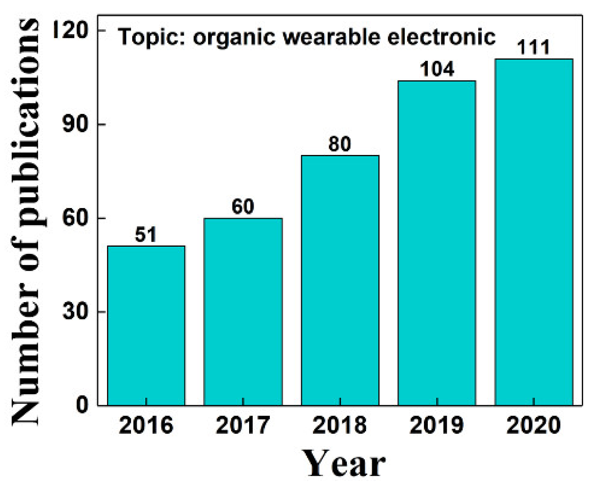
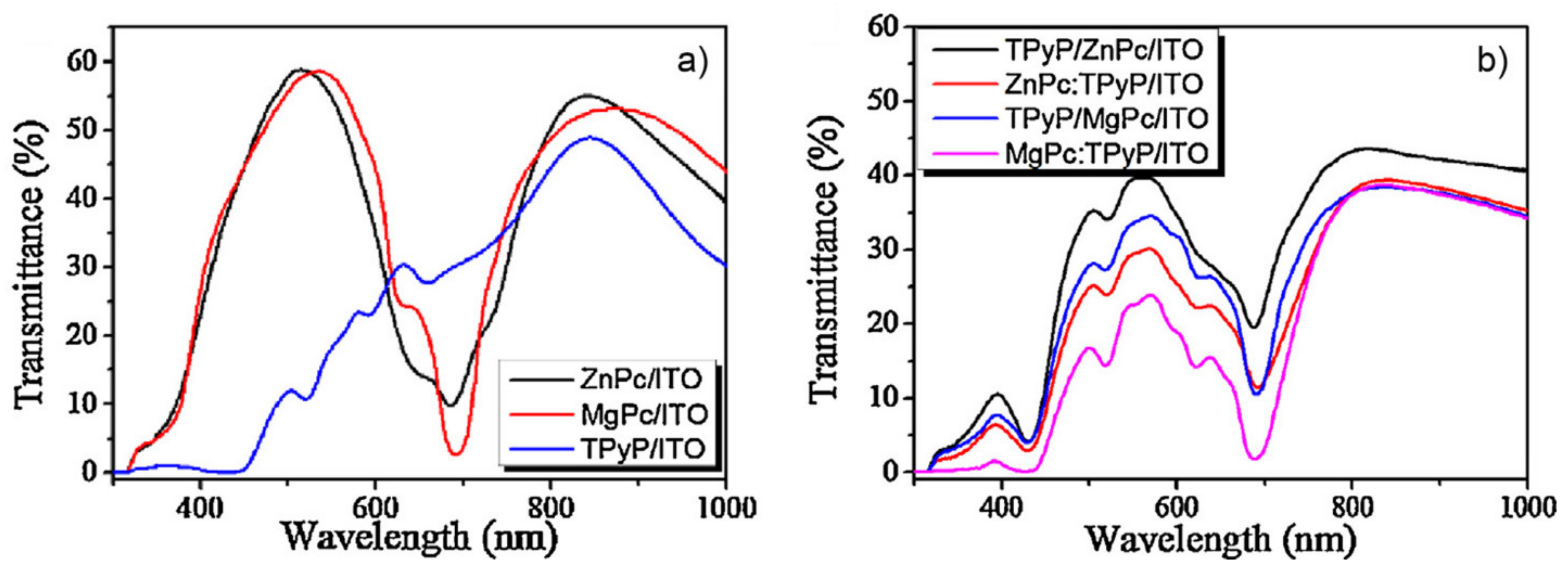
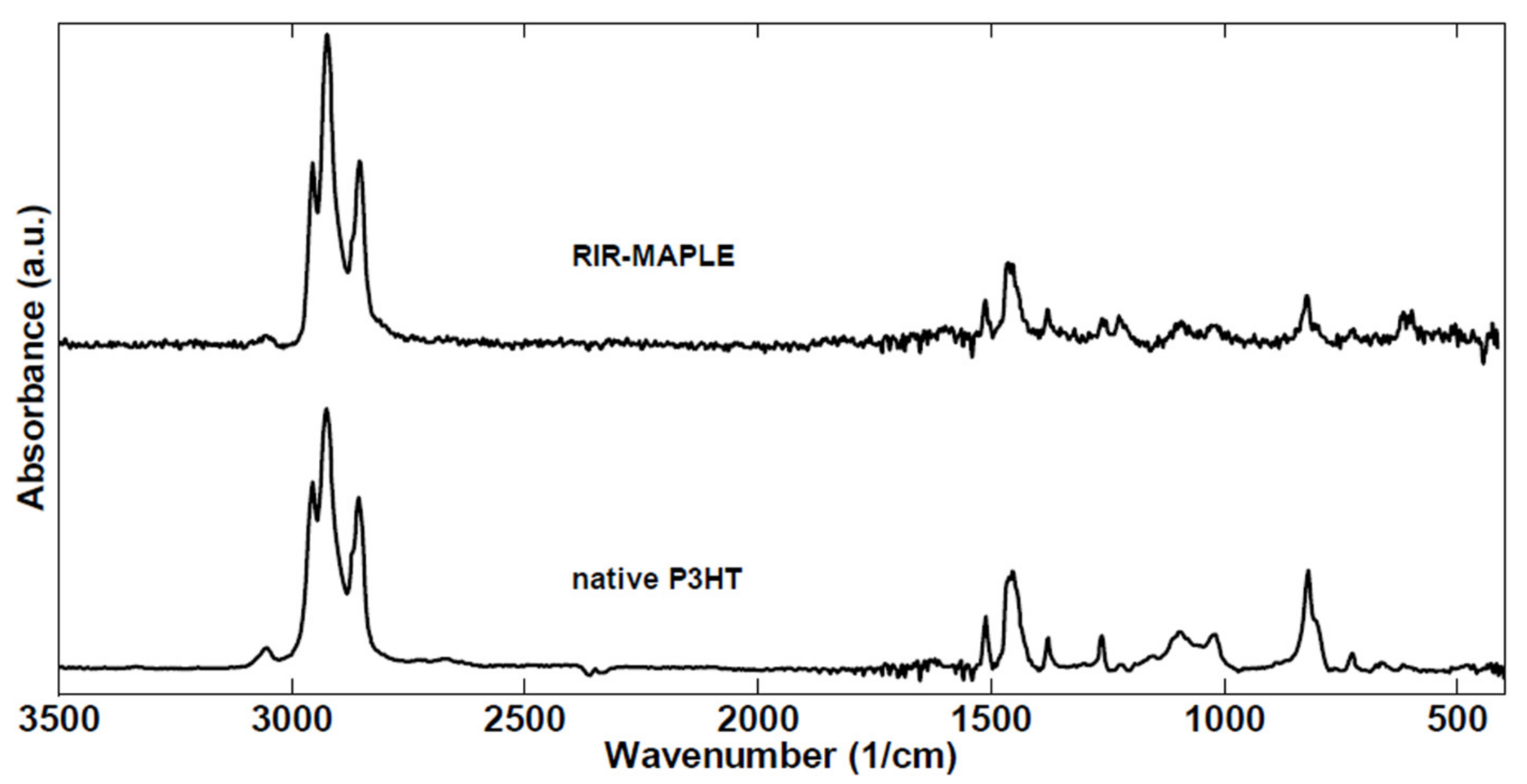
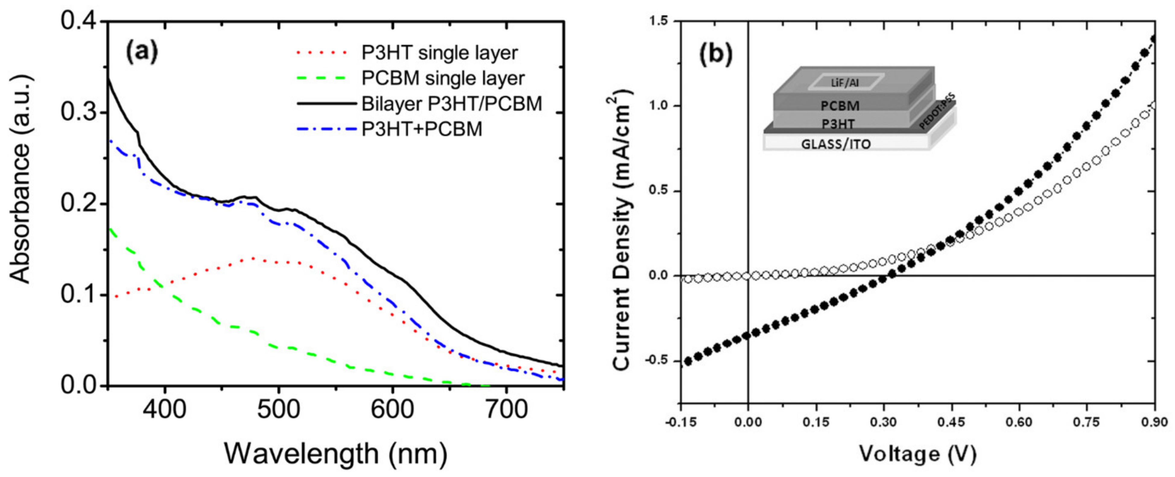
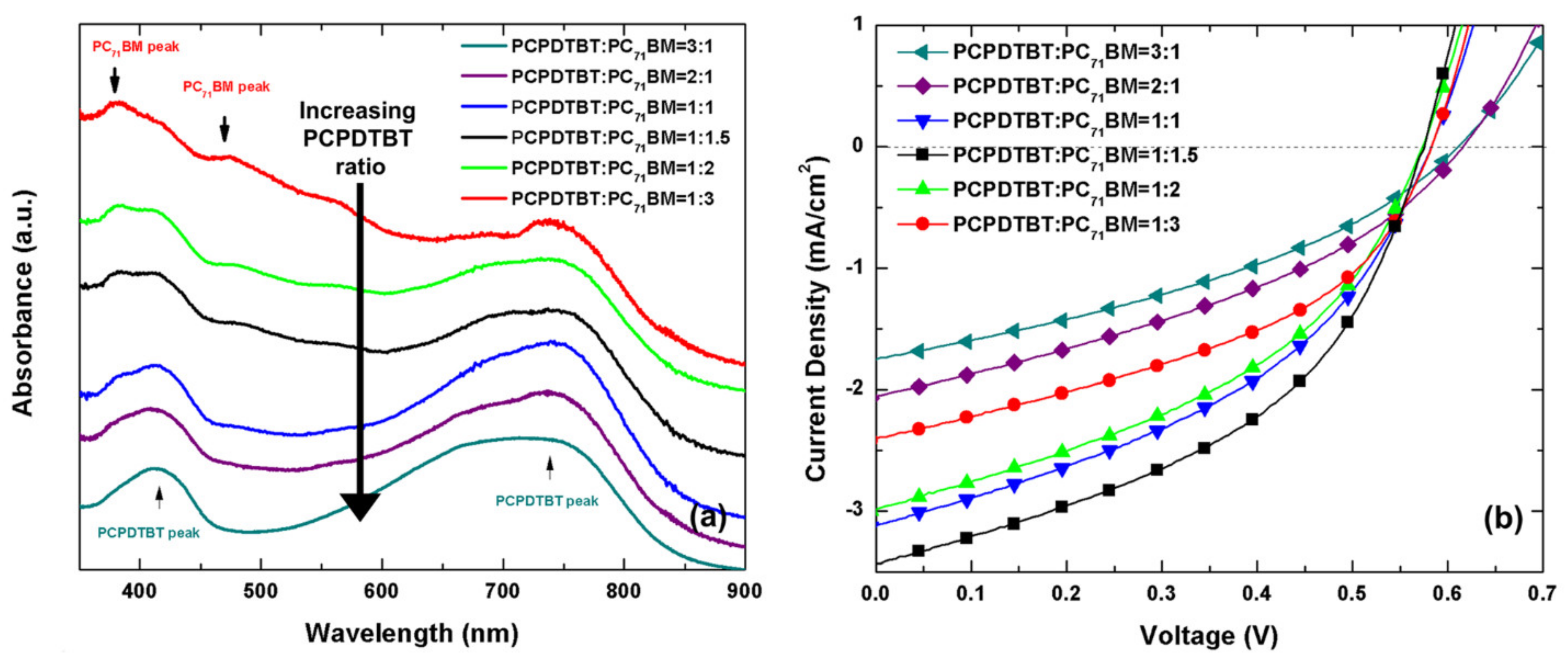
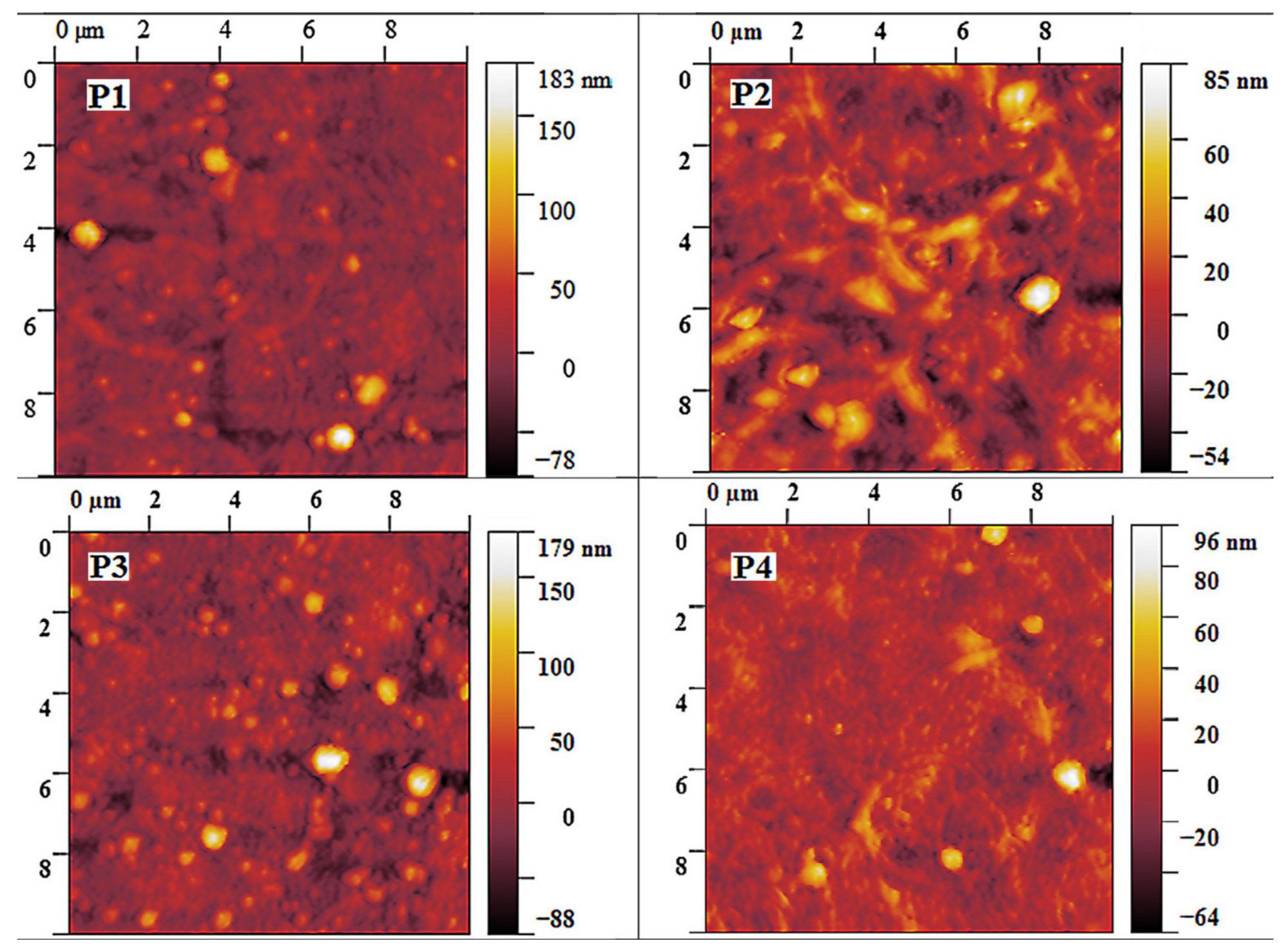
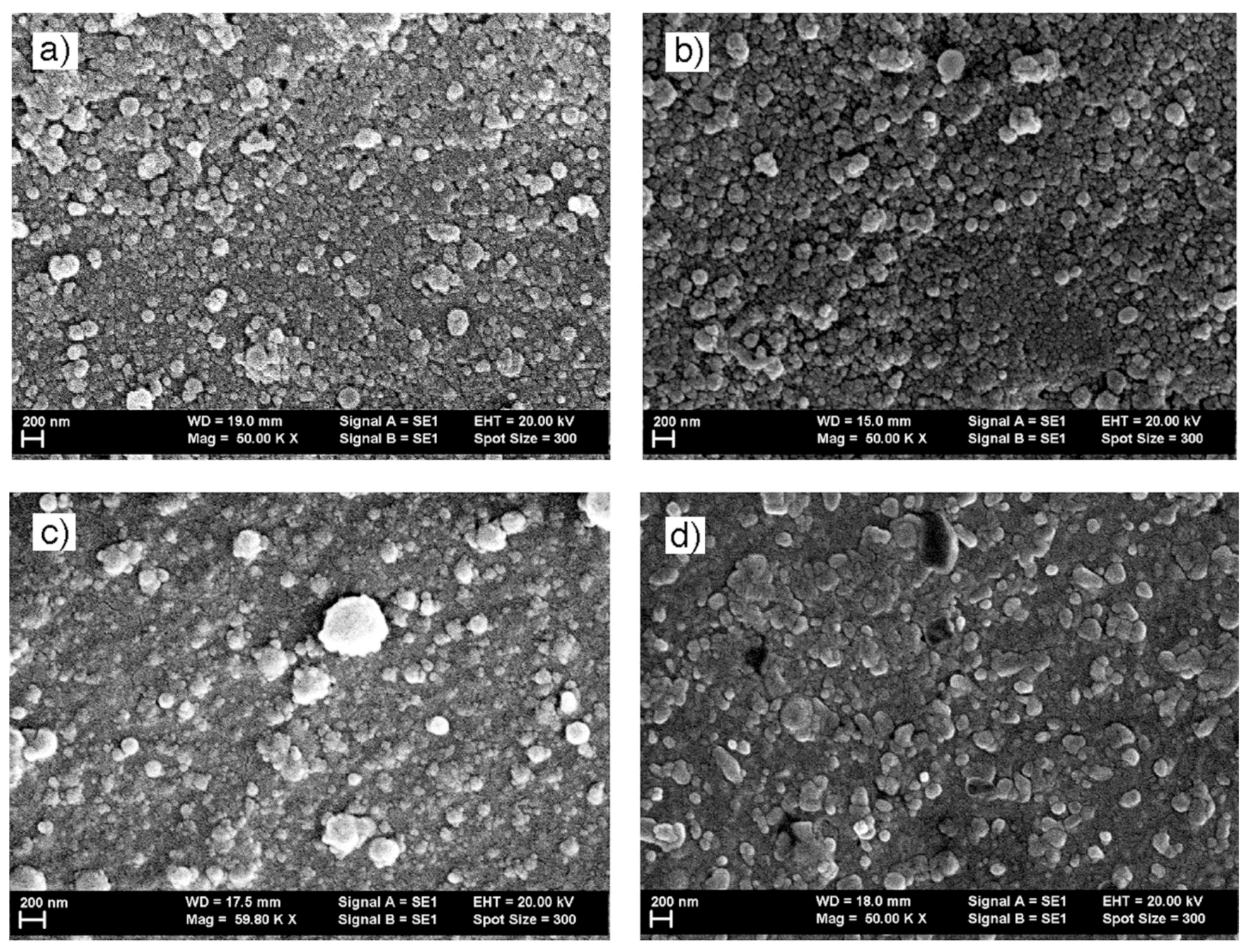
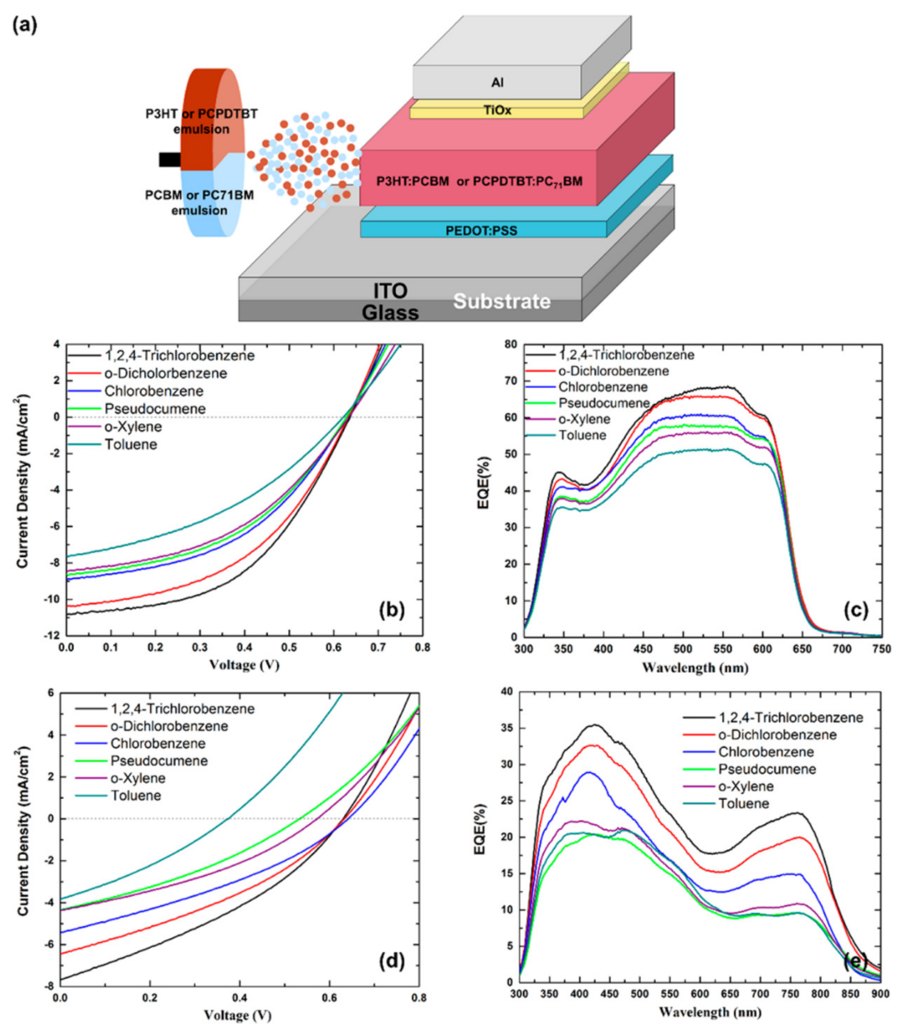
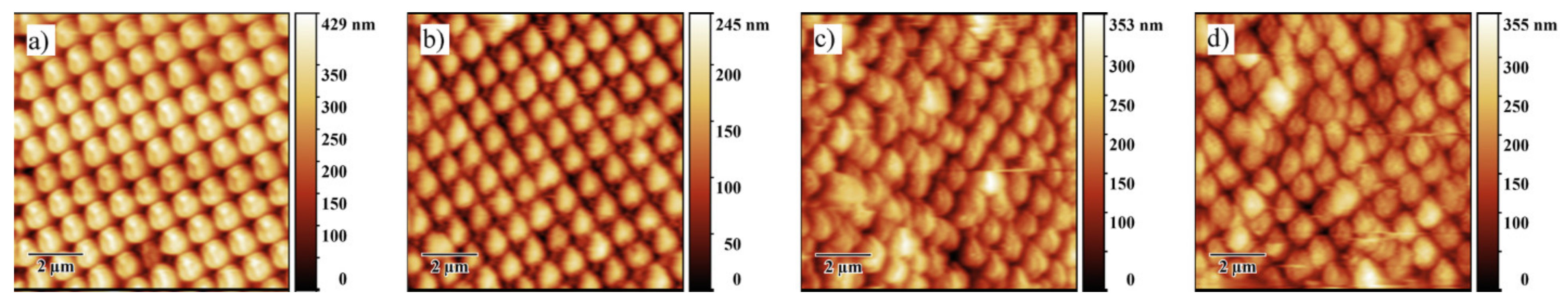
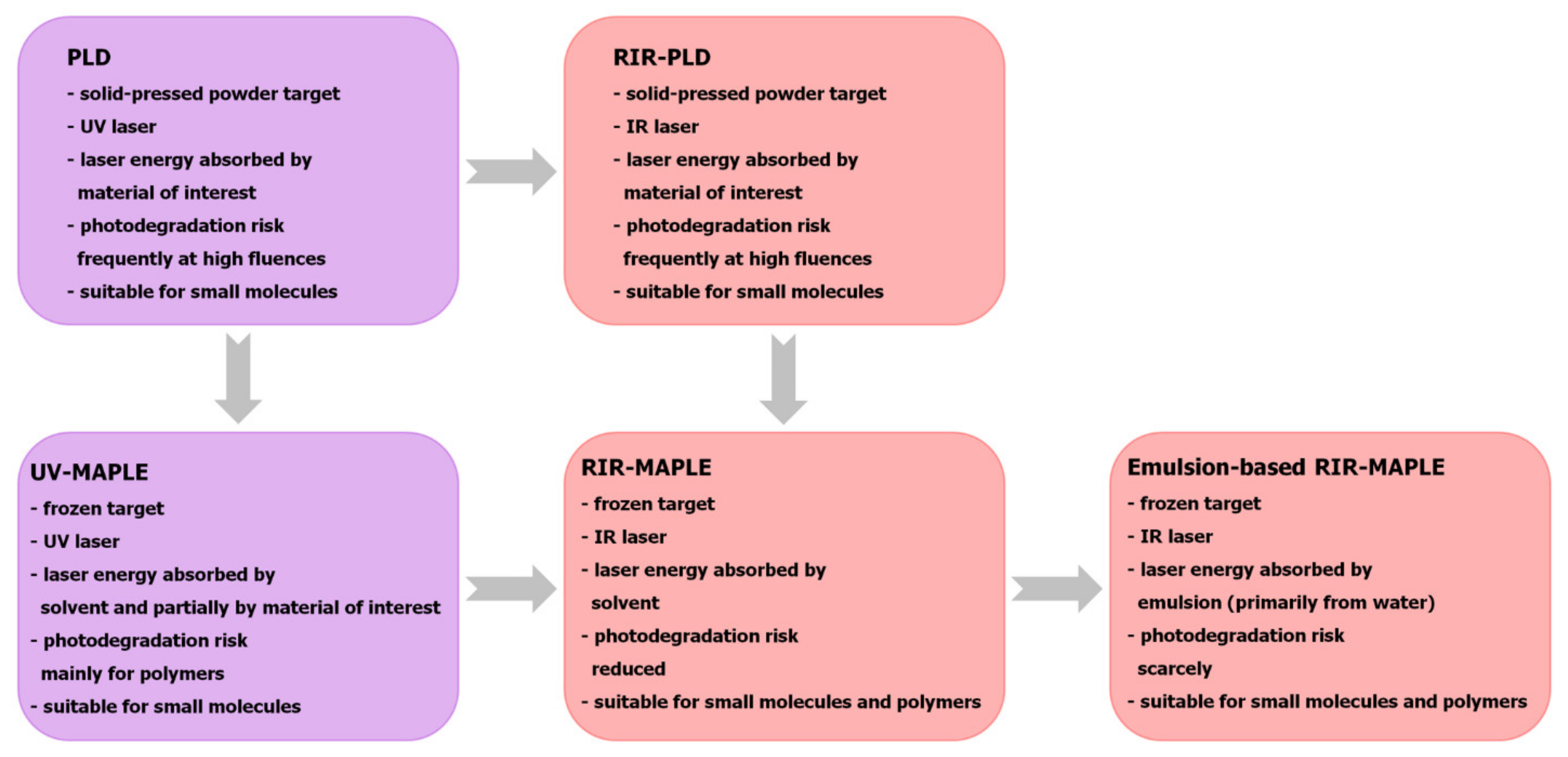
Table 1.
Organic thin films deposited using MAPLE-based techniques for PV applications: the organic compounds deposited as layers, the solvents used as a host matrix, concentration of the organic compound, laser wavelength and laser fluence used in the MAPLE deposition, the year when the work was reported (based on the data from the literature review).
| Organic Compounds | Solvent for Host Matrix | Concentration of the Organic Compound in the Primary Solvent | Laser Wavelength | Laser Fluence | Published Year | Ref. |
|---|---|---|---|---|---|---|
| MEH-PPV | THF * | 0.3 wt.% | 193 nm | <190 mJ/cm2 | 2004 | [49] |
| TOL * | ||||||
| THF | 0.3 wt.% | 248 nm | ||||
| TOL | ||||||
| CHL * | 8.2 μm | 0.5 J/cm2 | ||||
| P3HT | OX * | 0.8 wt.% | 266 nm | 200 mJ/cm2 | 2004 | [145] |
| MEH-CN-PPV | THF | 1 wt.% | 2.9 μm | 0.67–2 J/cm2 | 2008 | [61] |
| CB * | ||||||
| TOL | ||||||
| OX | ||||||
| CHL | ||||||
| PH *:THF | ||||||
| PH:DIW * | 0.25 wt.% | |||||
| MEH-PPV | THF | 1 wt.% | ||||
| TOL | ||||||
| CHL | ||||||
| PH:THF | ||||||
| PH:DIW | 0.25 wt.% | |||||
| MEH-CN-PPV | PH:DIW | 1 wt.% | 2.9 μm | 2 J/cm2 | 2009 | [143] |
| C60 | ANS * | 0.67 wt.% | 355 nm | 0.15–3.9 J/cm2 | 2011 | [139] |
| ZnPc | DMSO * | 2.5 g/L | 248 nm | 433 mJ/cm2 | 2011 | [115] |
| PTCDA | DMSO | 2.5 g/L or 4 g/L | 333–400 mJ/cm2 | |||
| Alq3 | CHL | 4 g/L | 166 or 433 mJ/cm2 | |||
| DMSO | 2.5 g/L | 350 mJ/cm2 | ||||
| PEDOT:PSS | NMP * | 1.2–1.4 wt.% | 3 µm | 2 J/cm2 | 2011 | [48] |
| P3HT/PCBM | TOL | 0.3 wt.% | 248 nm | 250 mJ/cm2 | 2012 | [38] |
| P3HT MEH-PPV | TOL:PH:DIW | 1 wt.% | 2.94 μm | Not mentioned | 2012 | [150] |
| C60 | ANS | 0.67 wt.% | 355 nm | 0.5–4 J/cm2 | 2013 | [140] |
| ZnPc NTCDA | DMSO | 2.5 g/L | 248 nm | 300 or 400 mJ/cm2 | 2014 | [135] |
| IT77:PCBB | CHL | 1 g/L or 3 g/L | 248 nm | 250 or 300 mJ/cm2 | 2014 | [120] |
| PCPDTBT:PC71BM | CB *:PH: DIW:SLS | 1 wt.% | 2.94 μm | 2 J/cm2 | 2014 | [69] |
| P3HT | solvent:PH: alcohol:DIW | 0.5 wt.% | 2.9 μm | 1.46–1.6 J/cm2 | 2014 | [144] |
| AMC16 AMC22 AMC16:C60 AMC22:C60 | CHL | 3 g/L | 248 nm | 250 mJ/cm2 | 2015 | [88] |
| P3HT | ODCB *:BA *: DIW:SDS * | 5 mg/mL | 2.94 μm | 1.3 J/cm2 | 2015 | [146] |
| P3HT | ODCB:BA: DIW:SDS | 1 wt.% | 2.94 μm | 1.7 J/cm2 | 2015 | [154] |
| PCPDTBT | CB:PH: DIW:SDS | |||||
| ODCB:PH: DIW:SDS | ||||||
| TCB *:PH: DIW:SDS | ||||||
| ZnPc/TPyP ZnPc:TPyP MgPc/TPyP MgPc:TPyP | DMSO | 2.5 g/L | 248 nm | 300 mJ/cm2 | 2016 | [40] |
| LS13:C60 LS78:C60 | ODCB | 4 g/L | 248 nm | 300 mJ/cm2 | 2016 | [153] |
| P3HT:PCBM PCPDTBT:PC71BM | TL *:PH:DIW | 5 mg/mL | 2.94 μm | 1.8 J/cm2 | 2016 | [70] |
| OX:PH:DIW | ||||||
| PDC:PH:DIW | ||||||
| CB:PH:DIW | ||||||
| ODCB:PH:DIW | ||||||
| TCB:PH:DIW | ||||||
| rubrene | TOL | 0.23–1 wt.% | 266 nm or 1064 nm | 0.22–10.37 J/cm2 | 2017 | [141] |
| XL | ||||||
| DCM | ||||||
| DCE | ||||||
| LV4:C61 LV5:C61 | CHL | 3 g/L | 248 nm | 312 mJ/cm2 | 2017 | [123] |
| DMSO | ||||||
| P3HT:C60 | TOL | 3 g/L | 248 nm | 250 mJ/cm2 | 2017 | [152] |
| P3HT | ODCB:BA: DIW:SDS | 5 mg/mL | 2.94 μm | 1.3 J/cm2 | 2017 | [37,147,148] |
| ZnPc | DMSO | 3 g/L | 248 nm | 250 mJ/cm2 | 2018 | [142] |
| PTCDA | 3 g/L | |||||
| Alq3 | 1.5 g/L | |||||
| P3HT | ODCB:BA: DIW:SDS | 5 mg/mL | 2.94 μm | 1.3 J/cm2 | 2018 | [149,151] |
| ZnPc:C60 ZnPc:PC70BM ZnPc:PC70BM:rubrene | DMSO | 3 g/L | 248 nm | 300 mJ/cm2 | 2020 | [86] |
| IT77:AMC14 | DMSO | 3 g/L | 248 nm | 250 mJ/cm2 | 2020 | [85] |
| DPP-DTT:C60 | CHL | 3 g/L | 193 nm | 100 mJ/cm2 | 2020 | [87] |
| rubrene | DCE * | 0.3–0.7 wt.% | 1064 nm | 3–4.8 J/cm2 | 2021 | [117] |
* Tetrahydrofuran—THF; Toluene—TOL; Orthoxylene—OX; Anisole—ANS; Dimethyl sulfoxide—DMSO; Chloroform—CHL; 1,2 Dichlorobenzene—ODCB; Chlorobenzene—CB; Phenol—PH; Deionized water—DIW; N-methylpyrrolidone—NMP; Benzyl alcohol—BA; 1,2,4-Trichlorobenzene—TCB; Pseudocumene—PDC; Xylene—XL; Dichloromethane—DCM; 1,1-Dichloroethane—DCE.
Publisher’s Note: MDPI stays neutral with regard to jurisdictional claims in published maps and institutional affiliations. |
© 2021 by the authors. Licensee MDPI, Basel, Switzerland. This article is an open access article distributed under the terms and conditions of the Creative Commons Attribution (CC BY) license (https://creativecommons.org/licenses/by/4.0/).
Share and Cite
MDPI and ACS Style
Socol, M.; Preda, N.; Socol, G. Organic Thin Films Deposited by Matrix-Assisted Pulsed Laser Evaporation (MAPLE) for Photovoltaic Cell Applications: A Review. Coatings 2021, 11, 1368. https://doi.org/10.3390/coatings11111368
AMA Style
Socol M, Preda N, Socol G. Organic Thin Films Deposited by Matrix-Assisted Pulsed Laser Evaporation (MAPLE) for Photovoltaic Cell Applications: A Review. Coatings. 2021; 11(11):1368. https://doi.org/10.3390/coatings11111368
Chicago/Turabian StyleSocol, Marcela, Nicoleta Preda, and Gabriel Socol. 2021. "Organic Thin Films Deposited by Matrix-Assisted Pulsed Laser Evaporation (MAPLE) for Photovoltaic Cell Applications: A Review" Coatings 11, no. 11: 1368. https://doi.org/10.3390/coatings11111368
Note that from the first issue of 2016, this journal uses article numbers instead of page numbers. See further details here.