
SiGeSn Quantum Dots in HfO2 for Floating Gate Memory Capacitors
by
 , and
, and
Catalin Palade
1,*, 
Adrian Slav
1,
Ovidiu Cojocaru
1,2 ,
,
Valentin Serban Teodorescu
1,3,
Toma Stoica
1,
Magdalena Lidia Ciurea
1,3 and
and
Ana-Maria Lepadatu
1,*
1
National Institute of Materials Physics, 405A Atomistilor Street, 077125 Magurele, Romania
2
Faculty of Physics, University of Bucharest, 405 Atomistilor Street, 077125 Magurele, Romania
3
Academy of Romanian Scientists, 54 Splaiul Independentei, 050094 Bucharest, Romania
*
Authors to whom correspondence should be addressed.
Coatings 2022, 12(3), 348; https://doi.org/10.3390/coatings12030348
Submission received: 1 February 2022
/
Revised: 2 March 2022
/
Accepted: 3 March 2022
/
Published: 7 March 2022
(This article belongs to the Special Issue Nanocomposite Thin Film and Multilayers)
Abstract
:Group IV quantum dots (QDs) in HfO2 are attractive for non-volatile memories (NVMs) due to complementary metal-oxide semiconductor (CMOS) compatibility. Besides the role of charge storage centers, SiGeSn QDs have the advantage of a low thermal budget for formation, because Sn presence decreases crystallization temperature, while Si ensures higher thermal stability. In this paper, we prepare MOS capacitors based on 3-layer stacks of gate HfO2/floating gate of SiGeSn QDs in HfO2/tunnel HfO2/p-Si obtained by magnetron sputtering deposition followed by rapid thermal annealing (RTA) for nanocrystallization. Crystalline structure, morphology, and composition studies by cross-section transmission electron microscopy and X-ray diffraction correlated with Raman spectroscopy and C–V measurements are carried out for understanding RTA temperature effects on charge storage behavior. 3-layer morphology and Sn content trends with RTA temperature are explained by the strongly temperature-dependent Sn segregation and diffusion processes. We show that the memory properties measured on Al/3-layer stack/p-Si/Al capacitors are controlled by SiGeSn-related trapping states (deep electronic levels) and low-ordering clusters for RTA at 325–450 °C, and by crystalline SiGeSn QDs for 520 and 530 °C RTA. Specific to the structures annealed at 520 and 530 °C is the formation of two kinds of crystalline SiGeSn QDs, i.e., QDs with low Sn content (2 at.%) that are positioned inside the floating gate, and QDs with high Sn content (up to 12.5 at.%) located at the interface of floating gate with adjacent HfO2 layers. The presence of Sn in the SiGe intermediate layer decreases the SiGe crystallization temperature and induces the easier crystallization of the diamond structure in comparison with 3-layer stacks with Ge-HfO2 intermediate layer. High frequency-independent memory windows of 3–4 V and stored electron densities of 1–2 × 10¹³ electrons/cm2 are achieved.
1. Introduction
Group IV quantum dots (QDs) are attractive for non-volatile memories (NVMs) considering their compatibility with CMOS technology [1,2,3,4,5,6,7,8,9,10]. Additionally, QDs can tune NVM device parameters related to performance and stability by tailoring their size, density, and interface quality with embedding oxide [11,12,13,14]. As embedding matrix and gate oxide, the high-k dielectric HfO2 is suitable to be used in high-density NVMs. HfO2 is already used in the CMOS industry due to its high CMOS compatibility and high scalability [15], and shows potential as a gate dielectric layer for post-Si electronic devices as well [16]. HfO2 is also promising for integrated ferroelectric memory devices due to nanoscale ferroelectricity [17,18]. More than that, NVM performance can be further enhanced by the cumulative contribution of the ferroelectric HfO2 matrix besides that of Ge QDs charge storage centers [19]. By using a channel with Ge:HfO2 gate, ferroelectric gating of the metal-insulator transition in ultra-thin VO2 was also successfully demonstrated [20]. Using HfO2 instead of classical SiO2 in NVMs enables a lower oxide equivalent thickness, also ensuring higher charge retention, lower operating voltages, and large memory windows [21]. The phototunable charging and discharging effect of Ge nanocrystals (NCs) embedded in nanocrystallized HfO2 for photonic flash memories was also evidenced [22]. By facilitating the charge tunneling between Ge NCs and Si substrate due to photogenerated excitons, the memory window is increased. All these highlight the application fields of micro/nanoelectronics, industrial automation, portable devices, computer systems [1].
In this paper, we use alloy SiGeSn QDs as charge storage nodes with the advantages of a low thermal budget for formation, high stability, and adjustable composition. By adding little Si to GeSn, the already known Ge fast diffusion in oxides [14] and Sn diffusion and segregation [23] are controlled under optimal annealing conditions of temperature and duration, leading to efficiently increased NCs stabilization [24,25] and reduced strain. This ensures a strong quantum confinement effect in SiGeSn QDs that in turn allows a high charge storage efficiency. On the other hand, alloying with Sn leads to highly short-wave infrared (SWIR) photosensitivity [26,27] that can be further exploited for photonic flash memories enabling fast access speed and low energy consumption by optical control of threshold voltage shift [1].
Our approach for QDs-based NVM consists of preparing structures with trilayer configuration with SiGeSn QDs-based floating gate and HfO2 gate and tunnel oxides fabricated on Si wafer in which the charge is injected from Si substrate. Besides the above-mentioned advantages, HfO2 also plays the role of barrier for Ge and Sn diffusion, and tunnel and gate oxide layers play the role of spacers allowing to control QDs size [27,28]. The use of nanocrystallized HfO2 as a matrix for SiGeSn QDs enables a good separation of QDs to each other [14]. More than that, Sn presence decreases the crystallization temperature, making the fabrication of memories with SiGeSn QDs nodes to be more suitable in terms of CMOS compatibility due to the reduced thermal budget compared to Si and Ge NCs/QDs formation. On the other hand, by tuning component layer thicknesses, high versatility in tuning morphology parameters is achieved also through the versatility of magnetron sputtering deposition and rapid thermal annealing (RTA) nanostructuring by the large variation of technological preparation conditions and parameters (sputtering targets, powers and rates, atmosphere; RTA temperature, ramps, gas flows, gases) [14,19].
In this paper, we present for the first time MOS capacitor floating gate memories based on SiGeSn QDs in a 3-layer stack of gate HfO2/floating gate of SiGeSn QDs in HfO2/tunnel HfO2/ on a p-Si substrate. The 3-layer structures are obtained by magnetron sputtering deposition followed by RTA for nanostructuring. The crystalline structure, morphology and composition are investigated and correlated with the memory properties of Al/gate HfO2/SiGeSn-HfO2 floating gate/tunnel HfO2/p-Si/Al capacitors for different RTA conditions. The contribution of different SiGeSn-related charge storage centers to the memory effect is evidenced, i.e., SiGeSn-related trapping states (deep electronic levels) and low-ordering clusters for RTA at 325–450 °C, and crystalline SiGeSn QDs for 520 and 530 °C RTA. The highest memory windows of 3–4 V are obtained by the formation of two kinds of crystalline QDs, i.e., low Sn (2 at.%) content SiGeSn QDs positioned inside the floating gate and SiGeSn QDs with high Sn content up to 12.5 at.% at the interfaces with HfO2 layers. The stored electron density reaches up to 2 × 10¹³ electrons/cm2.
2. Materials and Methods
2.1. Sample Preparation
Our approach for QDs-based NVM capacitors consists of magnetron sputtering deposition (Surrey Nanosystems Gamma 1000 equipment, Surrey NanoSystems Ltd., Newhaven, UK) of 3-layer stacks of gate HfO2/SiGeSn-HfO2/tunnel HfO2/p-Si followed by nanostructuring using RTA (Annealsys AS-Micro rapid thermal processing system, Annealsys, Montpellier, France). Firstly, we deposit the thin HfO2 tunnel layer with a thickness in the 4–8 nm range by sputtering from HfO2 target (45–55 W RF power) on (100) p-Si substrates (7–14 Ωcm resistivity) that were previously cleaned using standard procedures [11]. Then, we co-deposit SiGe (25–35 W DC), Sn (3.5–10 W DC), and HfO2 from corresponding targets for the intermediate layer (7–12 nm) that will play the role of the floating gate, and finally, sputter a thick 16–21 nm gate HfO2 layer. The intermediate layer has the composition of 10% Sn: 90% SiGe (vol.) and 80% SiGeSn: 20% HfO2 (vol.) estimated from the equivalent thicknesses based on the XRR calibration deposition rates of Sn (~0.5 nm/min), SiGe (~4.0 nm/min), and HfO2 (~1.2 nm/min); 5% Si: 95% Ge (at.) is the atomic composition of the SiGe target (provided by Kurt J. Lesker Company Ltd., East Sussex, Hastings, United Kingdom). In this work, we will present results on structures M1 and M2 with slightly different designed thicknesses of 16–17/9–10/7–8 nm and 20–21/11–12/6–7 nm, respectively, for the gate oxide/intermediate layer/tunnel oxide stack.
The obtained HfO2/SiGeSn–HfO2/HfO2/p-Si amorphous stacks are thermally treated by RTA in N2 (6N purity) for nanostructuring of the floating gate, i.e., formation of SiGeSn NCs/QDs as charge storage nodes in HfO2. Samples are RTA annealed in the 325–600 °C temperature range for 2–15 min. RTA also leads to HfO2 nanostructuring.
Finally, MOS capacitors are obtained by depositing top and bottom Al electrodes using thermal evaporation. Shadow masks with 1 mm × 1 mm areas were used for top Al contacts deposition.
2.2. Measurement Methods
Samples’ crystalline structure, morphology and composition were investigated by X-ray diffraction (XRD—Rigaku SmartLab, Rigaku, Tokyo, Japan), cross-section transmission electron microscopy (XTEM—Jeol JEM-ARM 200F electron microscope, JEOL Ltd., Tokyo, Japan), and Raman spectroscopy (Horiba LabRAM HR Evolution μ-Raman spectrometer with 325 nm laser excitation, HORIBA France SAS, Loos, France).
The memory properties of Al/gate HfO2/SiGeSn-HfO2 floating gate/tunnel HfO2/p-Si/Al capacitors were studied by measurements of capacitance–voltage (C–V) hysteresis loops at frequencies of 100, 500 and 1 MHz using a precision LCR meter (Agilent 4980A, Agilent Technologies, Inc., Santa Clara, CA, USA.). The hysteresis loop was measured in a quasi-static regime with 0.1 V/0.5 s steps by sweeping from +U to −U voltage and back. Before measuring each hysteresis branch, charging at the ends of the cycle was done for 1–5 min at +U and −U, respectively.
3. Results and Discussion
3.1. Crystalline Structure, Morphology and Composition Studies
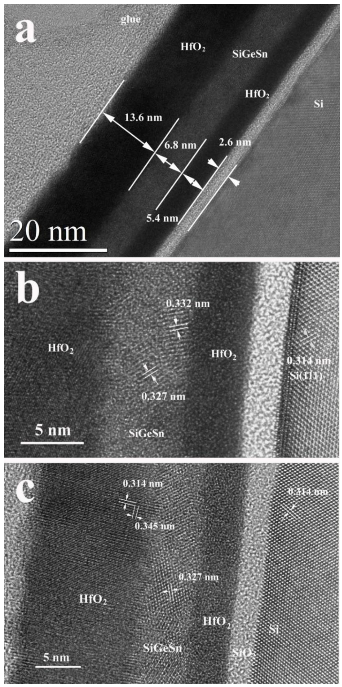
High resolution TEM (HRTEM) results. Figure 1 shows HRTEM images for a trilayer structure M1 annealed at 530 °C for 10 min (sample called M1-530-10 in the function of RTA temperature and duration). The designed thicknesses for as-deposited structure M1 are 16–17 nm for the gate oxide, 9–10 nm for the intermediate layer and 7–8 nm for the tunnel oxide in agreement with the cross-section TEM image in Figure 1a. In the high-resolution TEM image in Figure 1b, two lattice fringes are evidenced in the floating gate and at the interface with adjacent layers, of d111 = 0.327 nm and d111 = 0.332 nm, respectively, with an absolute error of 0.002 nm. It is known that lattice fringes corresponding to pure Si, Ge, and α-Sn are 0.314, 0.326, and 0.375 nm, respectively. Based on d111 values, we calculated the Sn content y for strain-relaxed SixGe1−x−ySny NCs (with Si content x of 5 at.%,) by using relationship a = 31/2d111 = 0.56575(1 − x − y) + 0.54307x + 0.64912y for the lattice constant. The a value was calculated by Vegard’s law [29] considering the lattice constants of Ge, Si, and Sn (0.56575, 0.54307, and 0.64912 nm, respectively). We obtain y = 2.1 at.% for d111 = 0.327 nm (close to pure Ge with plane spacing of 0.326, corresponding to the compensation by Sn alloying of the 5% Si mismatch in SiGe) and y = 12.5 at.% for d111 = 0.332 nm. This means the formation of low Sn content SiGeSn QDs in the floating gate, and the formation of SiGeSn QDs with high Sn content of 12.5% at the interface of the floating gate with adjacent layers (gate and tunnel HfO2). We remark that the Ge:Sn atomic ratio measured by EDX in the intermediate layer is ~4.3 in good agreement with HRTEM results.
The much higher Sn content at the interface of the floating gate with adjacent layers can be explained by Sn diffusion to the floating gate interfaces and by considering that Sn presence favors the SiGeSn crystallization process (decreasing SiGe crystallization temperature).
So, the SiGeSn QDs are rich in Ge (~90%) and have about 5 nm diameter. The density of QDs with high Sn content (12.5% Sn) is high enough to be also detected by Raman and XRD measurements and to contribute to the memory window widening as shown below.
Finally, the HRTEM image from Figure 1c shows the monoclinic structure of gate HfO2, the diamond structure of SiGeSn-based floating gate and the amorphous tunnel HfO2 layer. A plausible reason for maintaining the amorphous structure of tunnel HfO2 would seem to be the Sn diffusion at the interfaces of the floating gate with HfO2 layers. The top gate oxide layer is free to nucleate the HfO2 crystallization at the free surface, and the crystal growth is coherent in the whole layer thickness. The size of HfO2 NCs in the gate oxide layer is between 10 and 12 nm (HRTEM images). At the same time, the Si presence in the SiGeSn-based intermediate layer stops the Ge diffusion into the HfO2 layers. For this reason, we do not observe the HfO2 orthorhombic structure in the HfO2 layer, as is the case of 3-layer stacks with Ge-HfO2 intermediate layer [18].
The presence of Sn in the SiGe intermediate layer induces the easier crystallization of the diamond structure. This is in contrast to 3-layer stacks with Ge-HfO2 intermediate layer in which Ge QDs with a hexagonal crystalline structure are formed by topotactic crystallization on the HfO2 structure with corresponding tetragonal/orthorhombic lattice [14].
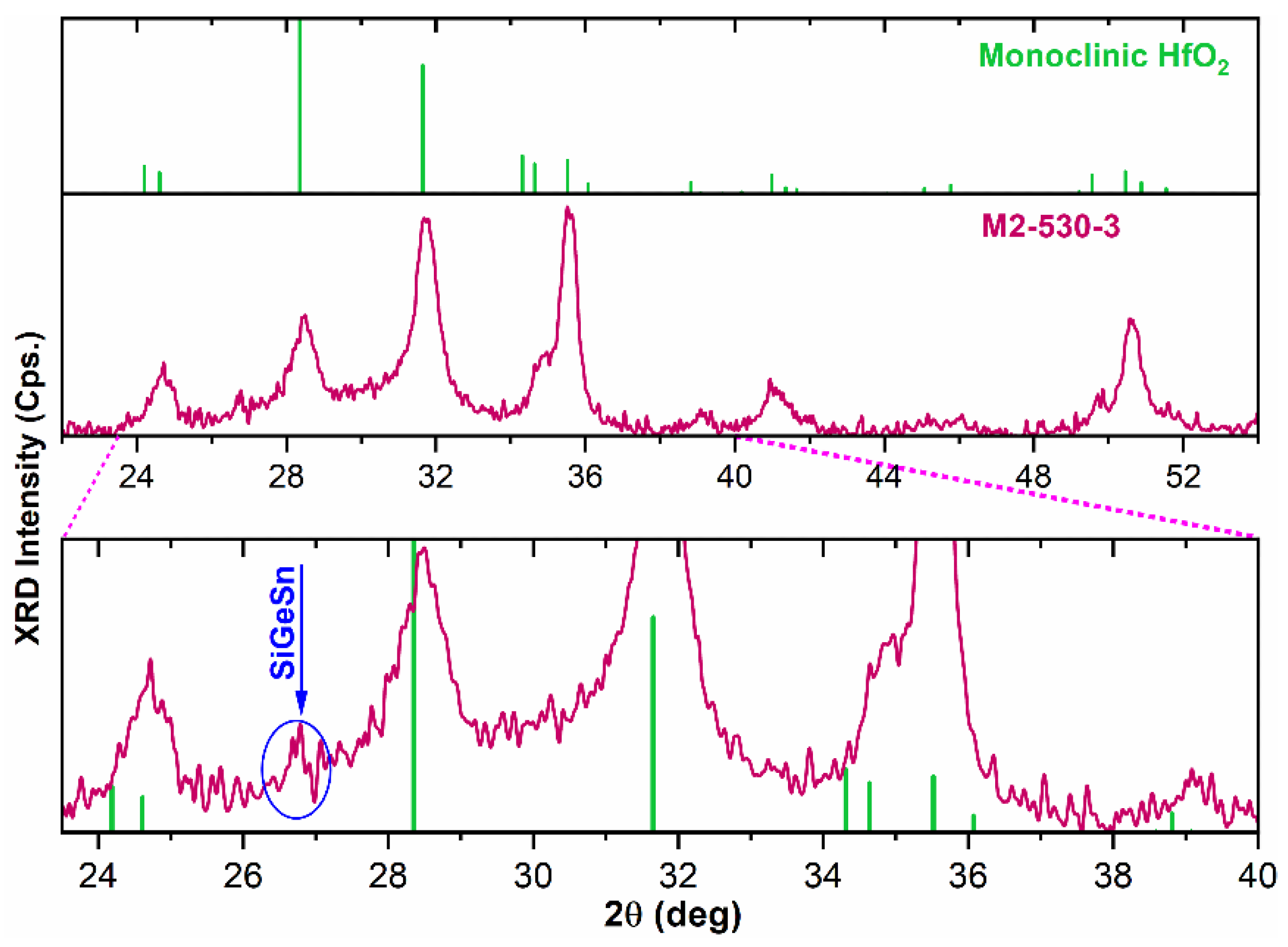
XRD results. Figure 2 shows an XRD diffractogram obtained on an annealed sample M2 with designed thicknesses for the as-deposited structure of 20–21 nm for the gate oxide, 11–12 nm for the floating gate and 6–7 nm for the tunnel oxide. The trilayer was annealed at 530 °C for 3 min (called M2-530-3). High-intensity XRD peaks correspond to monoclinic nanocrystallized HfO2 (according to PDF 01-078-0049). The estimated size of HfO2 NCs from the width of X-ray diffraction lines is in the 8–12 nm range in good agreement with HRTEM results.
Even if the SiGeSn equivalent thickness is relatively small for XRD, however, a small intensity feature related to (111) diamond line, seen as a shoulder of (−111) HfO2 maximum and being positioned at about 26.8 deg was detected. The 26.8 deg evaluated position corresponds to a lower 2θ value in comparison to Ge (tabulated 27.28 deg in PDF 00–004–0545) and Si (28.445 deg in PDF 01−070−5680) [25], and to higher 2θ values than α-Sn (23.7 deg in PDF 00−005−0390) [23] showing the formation of Ge-rich SiGeSn NCs in good agreement with HRTEM and Raman results (Section 3.2). The SiGeSn (111) peak position of 26.8 deg corresponds to the interplanar distance d111 with a mean value of 0.332 nm similar to the HRTEM results lattice (Figure 1b).
3.2. RTA Temperature Effects
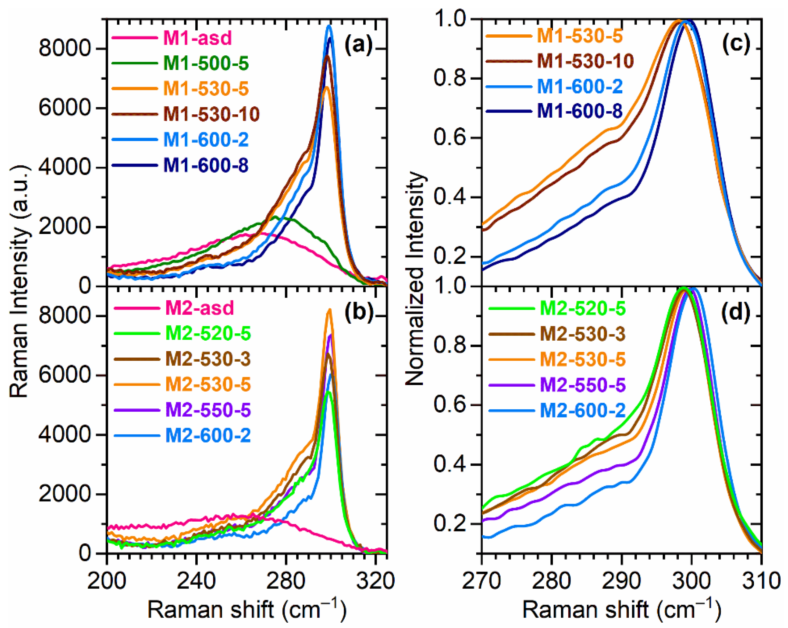
Raman scattering. Raman spectroscopy was carried out by using ultraviolet (UV) excitation laser emitting at 325 nm. The use of UV excitation has the advantage of a stronger absorption in the SiGeSn containing layer (floating gate) and thus to less penetrate in the bulk Si substrate lowering its 2TA contribution to the spectrum, altering by superposition the evidencing of Ge-Ge peak as in the case of using low absorption light of longer wavelength excitation (e.g., 633 nm). Figure 3 shows spectra obtained on structures M1 (16–17/9–10/7–8 nm) and M2 (20–21/11–12/6–7 nm) annealed at different temperatures for different durations (Table 1). The Ge-Ge vibration’s Raman signal is within the 200–320 cm−1 range. One can see that the RTA temperature of 500 °C is not enough for the formation of SiGeSn NCs, and the Raman spectra show a broad band corresponding to clusters formation at the start of nanocrystallization (Figure 3a). By annealing structures M1 at 530 and 600 °C, a sharp Raman peak corresponding to NCs formation is detected, meaning that the SiGeSn-based floating gate crystallizes (Figure 3a,c). In a similar way to Ge acting in SiGe alloys [28], the Sn alloying of Ge reduces the crystallization temperature, below 400 °C [23]. In our case, the small amount of Si in GeSn increases the crystallization temperature to about 530 °C. By increasing the RTA temperature from 530 to 600 °C, the Ge-Ge maximum narrows and shifts towards higher wave numbers. The Raman behavior of structures M2 (Figure 3b,d) is similar to structures M1.
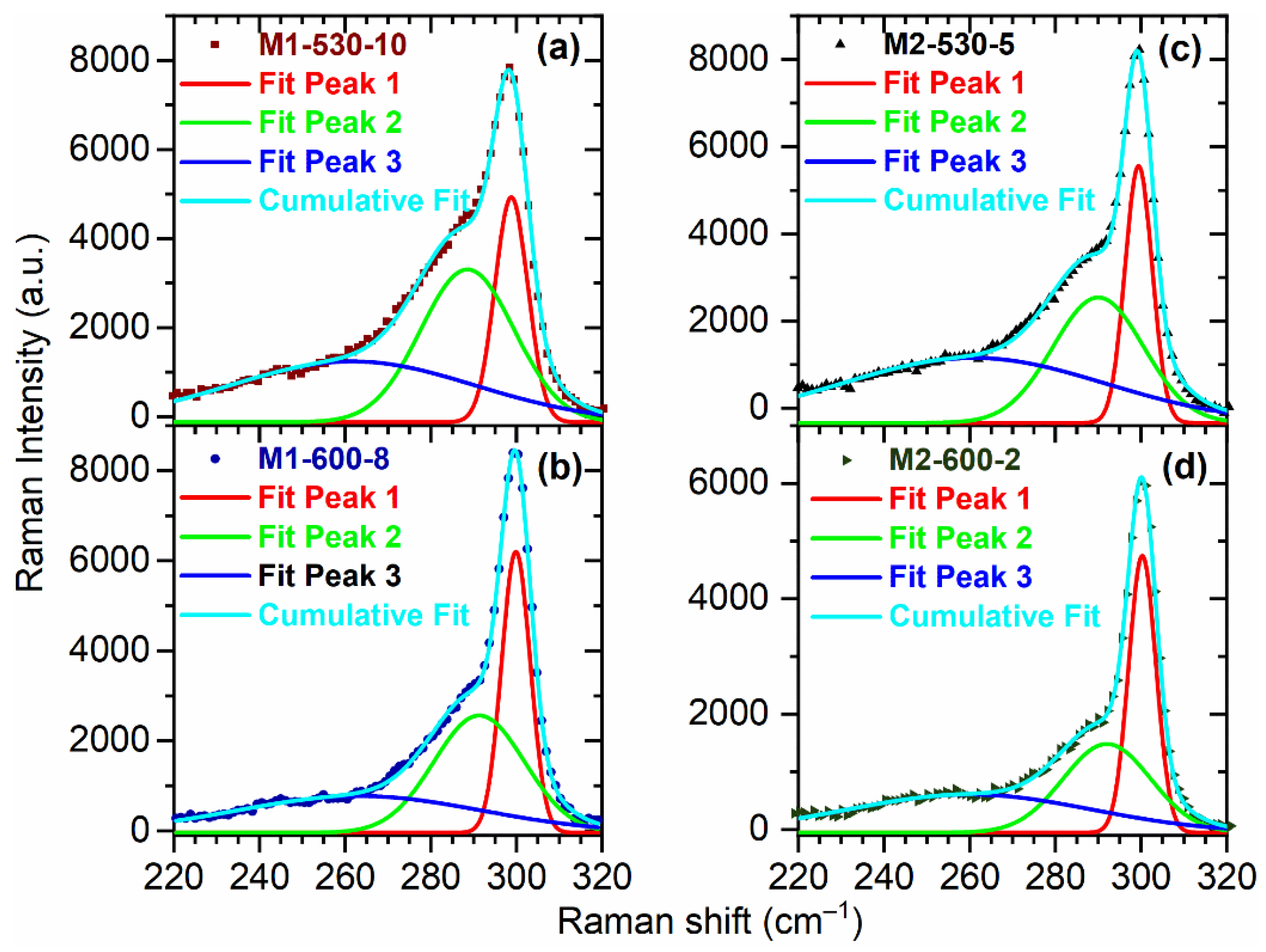
By deconvolution in the 220–320 cm−1 range of 3 Gauss peaks of the Raman spectra corresponding to M1 and M2 samples with nanocrystallized SiGeSn (by RTA at 520, 530, 550, and 600 °C), we obtain the results from Table 1.
Examples of deconvolution for 530 and 600 °C RTA structures M1 and M2 are illustrated in Figure 4. The most intense Gauss Peak 1 (red) corresponds to Ge-Ge vibration mode in SiGeSn NCs with low Si and Sn content, being positioned around 300 cm−1. Peak 2 (green) centered around 290 cm−1 describes the Ge-Ge mode in SiGeSn NCs with higher Sn content. This is in good agreement with HRTEM results, i.e., formation of low Sn content SiGeSn QDs in the floating gate, and formation of SiGeSn QDs with high Sn content of 12.5% at the interface of floating gate with adjacent HfO2 layers. The last Peak 3 (blue), practically a low-intensity broad band centered at about 260 cm−1 corresponds to low ordering, i.e., formation of clusters or amorphous SiGeSn nanoparticles [25].
By considering the Peak 2 position wGe-Ge in the Raman spectrum, the Sn content y in SixGe1−x−ySny QDs was evaluated using the formula wGe-Ge = 301 − 19.2x − 93.5y in which the 301 cm−1 value corresponds to the Raman shift of Ge-Ge mode in bulk Ge [30]. We obtain 12% Sn in SiGeSn NCs in structures M1 annealed at 530 °C in good agreement with HRTEM. By RTA at 600 °C, the Sn content decreases (down to 10%) due to Sn diffusion enhanced by the higher RTA temperature [23]. Enhancement of Sn diffusion is also reflected in the decreasing trend of the area ratio of Peak 2 to Peak 3 with the increase of annealing temperature (Table 1). Structures M2 show similar Raman behavior (Figure 4c,d) that also shows the formation of two kinds of SiGeSn NCs, ones with small Sn and Si content (Peak 1) and others with high Sn content of 11% for RTA at 520–550 °C and 9% by RTA at 600 °C (Peak 2).
The observed Raman and Sn content trend with RTA temperature was also evidenced in GeSn NCs embedded in SiO2 [23]. By low RTA temperature that is high enough to form NCs, alloy NCs with high Sn content are formed in the first stage of crystallization due to faster segregation of Sn than Ge from the SiO2 matrix. For higher annealing temperatures, a separation of β-Sn phase from GeSn NCs (low miscibility of Ge and Sn) is accompanied by Sn diffusion toward film surface. Similar segregation and diffusion processes take place in the case of SiGeSn NCs formation in the HfO2 matrix of the 3-layer structure. Here, the Sn diffusion in intermediate SiGeSn-HfO2 layer toward its interfaces with tunnel and control HfO2 layers results in higher Sn concentration SiGeSn NCs at the interface, as revealed by HRTEM analysis. By higher RTA temperatures, nanocrystallization is enhanced, but at the same time, Sn phase separation and Sn (and Ge) diffusion into the tunnel and control layers is favored leading to the reduction of the Sn content and density of SiGeSn NCs. This could be the reason for the diminished memory window in the structures annealed at higher temperatures of 600 °C. Another phenomenon that can take place is the increase of the conductivity of the tunnel layer by Sn diffusion.
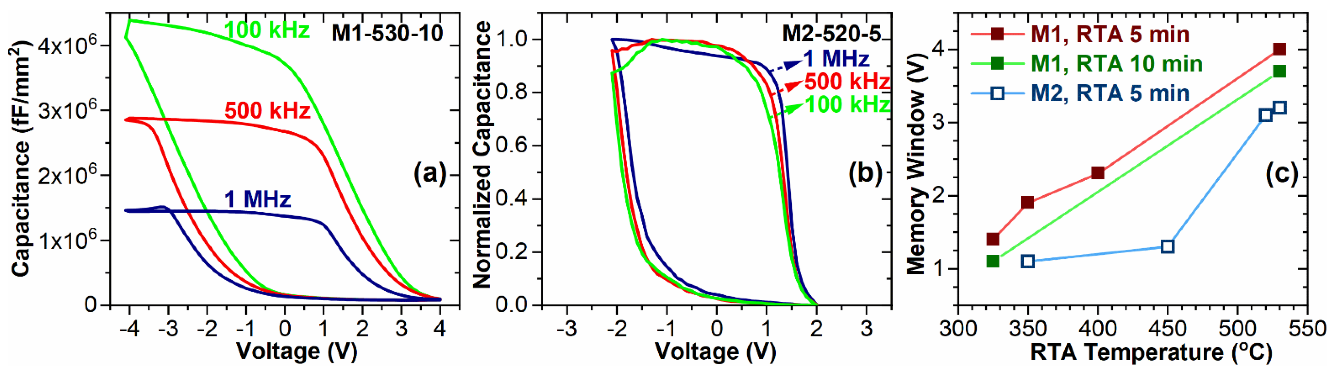
C–V hysteresis. Figure 5a,b illustrates typical C–V hysteresis loops measured on M1-530-10 and M2-520-5 capacitors at frequencies of 100 and 500 kHz and 1 MHz, with memory windows of 3.7 and 3.1 V, respectively. The memory capacitors present C–V hysteresis loops with counter-clockwise direction and frequency-independent memory window that are due to charge storage in SiGeSn QDs. Memory window ΔVfb was determined by considering the flat band voltage position at 80% of maximum capacitance from the C–V loops obtained on structures M1 and M2 annealed under different conditions of temperature and duration (Table 2). One can see from Figure 5c that the memory window increases with the increase of annealing temperature from 325 to 530 °C, the maximum values being obtained for RTA at 520 and 530 °C. Additionally, annealing for 5 min leads to obtaining slightly higher memory windows than for 10 min RTA.
Table 2 lists the memory window obtained on different structures M1 and M2. The highest memory windows are in the 3–4 V range, being produced by the charge storage in SiGeSn QDs subjected to RTA at temperatures of 520 and 530 °C favorable for diminished Sn phase separation and, consequently, to the formation of alloy SiGeSn NCs with high Sn content, in good agreement with Raman results. Structures M1 annealed at 530 °C, with the highest Sn content of 12% in SiGeSn QDs, show the highest memory windows of 4 and 3.7 V for 5 and 10 min RTA duration, respectively. Similarly, structures M2 annealed at 520 and 530 °C (5 min RTA) show the highest memory windows of 3.1 and 3.2 V, respectively.
Additionally, as one can see from Figure 5c and Table 2, there is an increase of the memory window with the increase of RTA temperature up to 530 °C (e.g., from 325 to 530 °C for structures M1 with 5 min RTA) reflecting the evolution of charge storage centers from SiGeSn-related trapping states (deep electronic levels) and low-ordering clusters for RTA at 325–450 °C to SiGeSn QDs for RTA at 520 and 530 °C [11]. As shown by Raman measurements, RTA temperatures under 500 °C are not enough for obtaining SiGeSn NCs, the 500 °C RTA leading to the formation of clusters at the start of nanocrystallization or amorphous SiGeSn nanoparticles. SiGeSn related states (deep energy levels) present in the amorphous structure and in clusters (low ordering) act as storage centers giving the main contribution to the memory effect (325–450 °C RTA).
The annealing at 520 and 530 °C leads to the formation of SiGeSn NCs (HRTEM, XRD and Raman) of two kinds, i.e., SiGeSn QDs with low Sn content (2 at.%) that are positioned inside the floating gate, and SiGeSn QDs with high Sn content (up to 12.5 at.%) located at the interface of the floating gate with the adjacent HfO2 layers. The main contribution of SiGeSn QDs as charge storage centers is demonstrated by the highest frequency-independent memory windows of 3–4 V with values similar to those for structures with the Ge QDs-based floating gate [14]. This is also correlated with the Sn content of QDs by the high area ratio of Raman Peak 2 (corresponding to QDs with 12 and 11 at.% Sn) to Peak 3 (for QDs SiGeSn NCs with low Si and Sn content—Table 1). The density of QDs with high Sn content is high enough to contribute to the memory window widening. The presence of Sn in the SiGe intermediate layer induces the easier crystallization of the diamond structure (decreasing the (Si)Ge crystallization temperature) in comparison with the 3-layer stacks with a Ge-HfO2 intermediate layer. More than that, Sn presence decreases the (Si)Ge crystallization temperature (from 600 to 520–530 °C RTA), making the fabrication of memories with SiGeSn QDs nodes to be more suitable in terms of CMOS compatibility.
RTA at higher temperatures of 600 °C leads to a pronounced decrease of a memory window. This can be explained by the high-temperature favored Sn diffusion leading to the reduction of the Sn content and density of SiGeSn NCs (reflected in decreased Sn content in QDs described by Raman Peak 2 that also has decreased area in comparison with Raman Peak 3 corresponding to QDs with low Sn content of 2%) or by the increase of the conductivity of layers by Sn diffusion in HfO2 layers. Besides, Ge fast diffusion is also more pronounced by increasing RTA temperature [13].
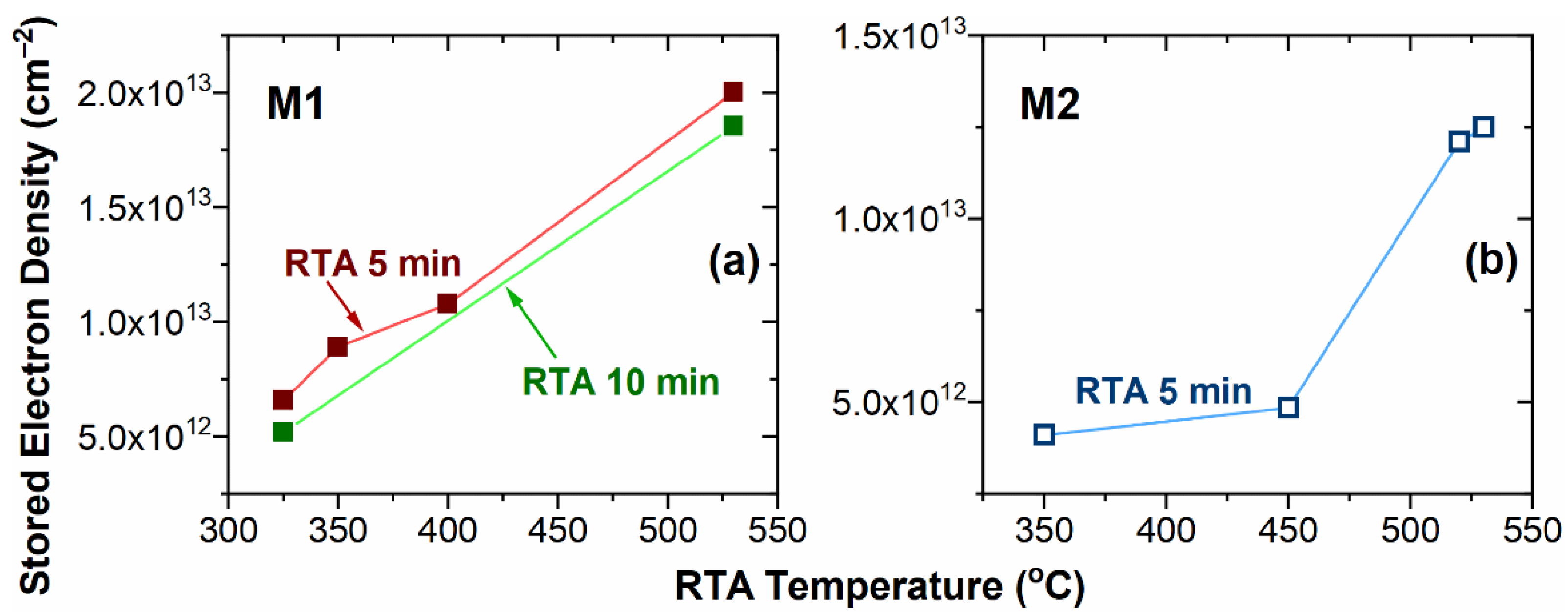
Based on the memory window ΔVfb results, we evaluated the stored electron density n (Table 2). Figure 6 illustrates the stored electron density versus RTA temperature for structures M1 and M2 annealed for 5 min, and structures M1 annealed for 10 min. As in the case of ΔVfb, the 5 min RTA leads to obtaining a slightly higher stored electron density than for 10 min RTA.
The stored electron density was evaluated by using the relation ΔVfb = (qn/ε0) × (dg/κg + dNC,FG/2κNC,FG) [22,31,32] considering the structure and the morphology of samples. So, for structures with crystallized floating gate (e.g., RTA at 520, 530 °C) of SiGeSn QDs in HfO2, the formula considers the diameter dNC and dielectric constant κNC of SiGeSn NCs charge storage centers, while for the structures with amorphous SiGeSn (RTA at 325–450 °C), thickness dFG and dielectric constant κFG of floating gate trapping layer are used instead [32]. The dielectric constants were extracted by simulation of frequency dispersion of capacitance and resistance measured in the accumulation regime [33].
One can see that the stored electron density is maximum for 520 and 530 °C, reaching 1–2 × 10¹³ electrons/cm2 for structures M1 and M2 in good agreement with the structure and morphology results that show the formation of dense SiGeSn QDs that act as charge storage centers.
The obtained charge storage results are promising for high-density NVMs based on highly CMOS compatible materials, i.e., the highly scalable high-k dielectric HfO2 and SiGeSn-related storage centers. More than that, the pathway to achieving simultaneous electrical and optical control of the memory effect by further optimization is also favored considering the high SWIR sensitivity demonstrated by alloying (Si)Ge with Sn in NCs based structures.
4. Conclusions
We have shown that specific to the 3-layer gate HfO2/SiGeSn-HfO2 floating gate/tunnel HfO2/p-Si stacks annealed at 520 and 530 °C is the formation of two kinds of crystalline SiGeSn QDs, i.e., low Sn content SiGeSn QDs (2 at.%) positioned in the floating gate and SiGeSn QDs with high Sn content up to 12.5 at.% located at the interface of the floating gate with adjacent HfO2 layers. The memory properties measured on Al/3-layer/p-Si/Al capacitors are controlled by SiGeSn-related trapping states (deep electronic levels) and low-ordering clusters for RTA at 325–450 °C, and by crystalline SiGeSn QDs for 520 and 530 °C RTA. The density of QDs with high Sn contents is high enough to contribute to the memory window widening, meaning high frequency-independent memory windows of 3–4 V and stored electron densities of 1–2 × 10¹³ electrons/cm2 are achieved. The results are promising for high-density electronic NVMs with extension to photonic memories based on highly CMOS compatible materials and low thermal budget fabrication.
Author Contributions
Conceptualization, all authors; Methodology, all authors; Validation, all authors; Investigation, C.P., A.S., O.C., V.S.T., T.S. and A.-M.L.; writing—original draft preparation, A.-M.L.; writing—review and editing, T.S., M.L.C. and A.-M.L.; supervision, A.-M.L. All authors have read and agreed to the published version of the manuscript.
Funding
This research was funded by CNCS—UEFISCDI, projects no. PN-III-P1-1.1-TE-2016-2366, PN-III-P4-ID-PCE-2020-1673, PN-III-P1-1.1-PD-2019-1038 and PN-III-P2-2.1-PED-2019-0205 within PNCDI III and by Romanian Ministry of Research, Innovation and Digitalization, NIMP Core Program PN19-03 Contract no. 21N/2019.
Institutional Review Board Statement
Not applicable.
Informed Consent Statement
Not applicable.
Data Availability Statement
Not applicable.
Conflicts of Interest
The authors declare no conflict of interest.
References
- Lv, Z.; Wang, Y.; Chen, J.; Wang, J.; Zhou, Y.; Han, S.T. Semiconductor quantum dots for memories and neuromorphic computing systems. Chem. Rev. 2020, 120, 3941–4006. [Google Scholar] [CrossRef] [PubMed]
- Lehninger, D.; Beyer, J.; Heitmann, J. A review on Ge nanocrystals embedded in SiO2 and high-k dielectrics. Phys. Status Solidi A 2018, 215, 1701028. [Google Scholar] [CrossRef]
- Fu, S.W.; Chen, H.J.; Wu, H.T.; Chuang, B.R.; Shih, C.F. Effect of hydrogen ion beam treatment on Si nanocrystal/SiO2 superlattice-based memory devices. Appl. Surf. Sci. 2016, 367, 134–139. [Google Scholar] [CrossRef]
- Mederos, M.; Mestanza, S.N.M.; Lang, R.; Doi, I.; Diniz, J.A. Germanium nanoparticles grown at different deposition times for memory device applications. Thin Solid Film. 2016, 611, 39–45. [Google Scholar] [CrossRef]
- Lien, Y.-C.; Shieh, J.-M.; Huang, W.-H.; Tu, C.-H.; Wang, C.; Shen, C.-H.; Dai, B.-T.; Pan, C.-L.; Hu, C.; Yang, F.-L. Fast programming metal-gate Si quantum dot nonvolatile memory using green nanosecond laser spike annealing. Appl. Phys. Lett. 2012, 100, 143501. [Google Scholar] [CrossRef] [Green Version]
- Olmedo, M.; Wang, C.; Ryu, K.; Zhou, H.; Ren, J.; Zhan, N.; Zhou, C.; Liu, J. Carbon nanotube memory by the self-assembly of silicon nanocrystals as charge storage nodes. ACS Nano 2011, 5, 7972–7977. [Google Scholar] [CrossRef]
- Rathore, J.S.; Fandan, R.; Srivastava, S.; Khiangte, K.R.; Das, S.; Ganguly, U.; Laha, A.; Mahapatra, S. Self-assembled Sn nanocrystals as the floating gate of nonvolatile flash memory. ACS Appl. Electron. Mater. 2019, 1, 1852–1858. [Google Scholar] [CrossRef]
- Vasilache, D.; Cismaru, A.; Dragoman, M.; Stavarache, I.; Palade, C.; Lepadatu, A.M.; Ciurea, M.L. Non-volatile memory devices based on Ge nanocrystals. Phys. Status Solidi A 2016, 213, 255–259. [Google Scholar] [CrossRef]
- Yu, J.; Chen, K.; Ma, Z.; Zhang, X.; Jiang, X.; Huang, X.; Zhang, Y.; Wang, L. Superior endurance performance of nonvolatile memory devices based on discrete storage in surface-nitrided Si nanocrystals. J. Appl. Phys. 2016, 119, 044507. [Google Scholar] [CrossRef]
- Bar, R.; Aluguri, R.; Manna, S.; Ghosh, A.; Satyam, P.V.; Ray, S.K. Multilayer Ge nanocrystals embedded within Al2O3 matrix for high performance floating gate memory devices. Appl. Phys. Lett. 2015, 107, 093102. [Google Scholar] [CrossRef]
- Stavarache, I.; Cojocaru, O.; Maraloiu, V.A.; Teodorescu, V.S.; Stoica, T.; Ciurea, M.L. Effects of Ge-related storage centers formation in Al2O3 enhancing the performance of floating gate memories. Appl. Surf. Sci. 2021, 542, 148702. [Google Scholar] [CrossRef]
- Ma, Z.; Wang, W.; Yang, H.; Jiang, X.; Yu, J.; Qin, H.; Xu, L.; Chen, K.; Huang, X.; Li, W.; et al. Performance and retention characteristics of nanocrystalline Si floating gate memory with an Al2O3 tunnel layer fabricated by plasma-enhanced atomic layer deposition. J. Appl. Phys. 2016, 119, 075702. [Google Scholar] [CrossRef]
- Slav, A.; Palade, C.; Lepadatu, A.M.; Ciurea, M.L.; Teodorescu, V.S.; Lazanu, S.; Maraloiu, A.V.; Logofatu, C.; Braic, M.; Kiss, A. How morphology determines the charge storage properties of Ge nanocrystals in HfO2. Scr. Mater. 2016, 113, 135–138. [Google Scholar] [CrossRef]
- Lepadatu, A.M.; Palade, C.; Slav, A.; Maraloiu, A.V.; Lazanu, S.; Stoica, T.; Logofatu, C.; Teodorescu, V.S.; Ciurea, M.L. Single layer of Ge quantum dots in HfO2 for floating gate memory capacitors. Nanotechnology 2017, 28, 175707. [Google Scholar] [CrossRef]
- Robertson, J.; Wallace, R.M. High-K materials and metal gates for CMOS applications. Mater. Sci. Eng. R 2015, 88, 1–41. [Google Scholar] [CrossRef] [Green Version]
- Lo Nigro, R.; Fiorenza, P.; Greco, G.; Schilirò, E.; Roccaforte, F. Structural and insulating behaviour of high permittivity binary oxides thin films for silicon carbide and gallium nitride electronic devices. Materials 2022, 15, 830. [Google Scholar] [CrossRef]
- Mikolajick, T.; Schroeder, U.; Slesazeck, S. The past, the present, and the future of ferroelectric memories. IEEE Trans. Electron. Devices 2020, 67, 1434–1443. [Google Scholar] [CrossRef]
- Palade, C.; Lepadatu, A.M.; Slav, A.; Cojocaru, O.; Iuga, A.; Maraloiu, V.A.; Moldovan, A.; Dinescu, M.; Teodorescu, V.S.; Stoica, T.; et al. A nanoscale continuous transition from the monoclinic to ferroelectric orthorhombic phase inside HfO2 nanocrystals stabilized by HfO2 capping and self-controlled Ge doping. J. Mater. Chem. C 2021, 9, 12353–12366. [Google Scholar] [CrossRef]
- Palade, C.; Slav, A.; Lepadatu, A.M.; Stavarache, I.; Dascalescu, I.; Maraloiu, A.V.; Negrila, C.; Logofatu, C.; Stoica, T.; Teodorescu, V.S.; et al. Orthorhombic HfO2 with embedded Ge nanoparticles in nonvolatile memories used for the detection of ionizing radiation. Nanotechnology 2019, 44, 445501. [Google Scholar] [CrossRef]
- Yajima, T.; Nishimura, T.; Tanaka, T.; Uchida, K.; Toriumi, A. Modulation of VO2 metal–insulator transition by ferroelectric HfO2 gate insulator. Adv. Electron. Mater. 2020, 6, 1901356. [Google Scholar] [CrossRef] [Green Version]
- Das, S.; Das, K.; Singha, R.K.; Dhar, A.; Ray, S.K. Improved charge injection characteristics of Ge nanocrystals embedded in hafnium oxide for floating gate devices. Appl. Phys. Lett. 2007, 91, 233118. [Google Scholar] [CrossRef]
- Palade, C.; Slav, A.; Lepadatu, A.M.; Maraloiu, A.V.; Dascalescu, I.; Iftimie, S.; Lazanu, S.; Ciurea, M.L.; Stoica, T. Optoelectric charging-discharging of Ge nanocrystals in floating gate memory. Appl. Phys. Lett. 2018, 113, 213106. [Google Scholar] [CrossRef]
- Slav, A.; Palade, C.; Logofatu, C.; Dascalescu, I.; Lepadatu, A.M.; Stavarache, I.; Comanescu, F.; Iftimie, S.; Antohe, S.; Lazanu, S.; et al. GeSn nanocrystals in GeSnSiO2 by magnetron sputtering for short-wave infrared detection. ACS Appl. Nano Mater. 2019, 2, 3626–3635. [Google Scholar] [CrossRef]
- Wirths, S.; Buca, D.; Mantl, S. Si–Ge–Sn alloys: From growth to applications. Prog. Cryst. Growth Charact. Mater. 2016, 62, 1–39. [Google Scholar] [CrossRef]
- Lepadatu, A.M.; Palade, C.; Slav, A.; Cojocaru, O.; Maraloiu, V.A.; Iftimie, S.; Comanescu, F.; Dinescu, A.; Teodorescu, V.S.; Stoica, T.; et al. Influence of SiGe nanocrystallization on short-wave infrared sensitivity of SiGe-TiO2 films and multilayers. J. Phys. Chem. C 2020, 124, 25043. [Google Scholar] [CrossRef]
- Miao, Y.; Wang, G.; Kong, Z.; Xu, B.; Zhao, X.; Luo, X.; Lin, H.; Dong, Y.; Lu, B.; Dong, L.; et al. Review of Si-based GeSn CVD growth and optoelectronic applications. Nanomaterials 2021, 11, 2556. [Google Scholar] [CrossRef]
- Slav, A.; Dascalescu, I.; Lepadatu, A.M.; Palade, C.; Zoita, N.C.; Stroescu, H.; Iftimie, S.; Lazanu, S.; Gartner, M.; Buca, D.; et al. GeSn/SiO2 multilayers by magnetron sputtering deposition for short-wave infrared photonics. ACS Appl. Mater. Interfaces 2020, 12, 56161–56171. [Google Scholar] [CrossRef]
- Palade, C.; Lepadatu, A.-M.; Slav, A.; Teodorescu, V.S.; Stoica, T.; Ciurea, M.L.; Ursutiu, D.; Samoila, C. Nano-crystallized Ge-rich SiGe-HfO2 highly photosensitive in short-wave infrared. Materials 2021, 14, 7040. [Google Scholar] [CrossRef]
- Moontragoon, P.; Pengpit, P.; Burinprakhon, T.; Maensiri, S.; Vukmirovic, N.; Ikonic, Z.; Harrison, P. Electronic properties calculation of Ge1−x−ySixSny ternary alloy and nanostructure. J. Non-Cryst. Solids 2012, 358, 2096–2098. [Google Scholar] [CrossRef]
- Fournier-Lupien, J.H.; Mukherjee, S.; Wirths, S.; Pippel, E.; Hayazawa, N.; Mussler, G.; Hartmann, J.M.; Desjardins, P.; Buca, D.; Moutanabbir, O. Strain and composition effects on Raman vibrational modes of silicon-germanium-tin ternary alloys. Appl. Phys. Lett. 2013, 103, 263103. [Google Scholar] [CrossRef] [Green Version]
- Kanoun, M.; Busseret, C.; Poncet, A.; Souifi, A.; Baron, T.; Gautier, E. Electronic properties of Ge nanocrystals for non volatile memory applications. Solid State Electron. 2006, 50, 1310–1314. [Google Scholar] [CrossRef]
- Maikap, S.; Lee, H.Y.; Wang, T.Y.; Tzeng, P.J.; Wang, C.C.; Lee, L.S.; Liu, K.C.; Yang, J.R.; Tsai, M.J. Charge trapping characteristics of atomic-layer deposited HfO2 films with Al2O3 as a blocking oxide for high-density non-volatile memory device applications. Semicond. Sci. Technol. 2007, 22, 884–889. [Google Scholar] [CrossRef] [Green Version]
- Palade, C.; Lepadatu, A.M.; Slav, A.; Lazanu, S.; Teodorescu, V.S.; Stoica, T.; Ciurea, M.L. Material parameters from frequency dispersion simulation of floating gate memory with Ge nanocrystals in HfO2. Appl. Surf. Sci. 2018, 428, 698–702. [Google Scholar] [CrossRef]
Figure 1.
XTEM results on structure M1-530-10: (a) low magnification cross-section TEM image revealing the thicknesses of component layers in the 3-layer stack structure; (b) HRTEM image evidencing lattice fringes d111 = 0.327 nm very close to pure Ge plane spacing (0.326 nm) in the floating gate, and d111 = 0.332 nm at the interface of floating gate with adjacent layers, respectively (with 0.314 nm (111) lattice distance measured in the Si substrate as the reference); (c) HRTEM image showing the monoclinic crystalline structure of HfO2 (e.g., 0.314 nm fringe) in the gate oxide layer, the amorphous structure in the tunnel layer, and a 5 nm SiGeSn crystallite in [110] orientation in the floating gate.

Figure 2.
XRD diffractogram of structure M2-530-3: high-intensity peaks correspond to monoclinic nanocrystallized HfO2 by comparing with PDF 01-078-0049 data (indicated in green on top of figure). A small intensity feature around 26.8 deg seen as a shoulder of (−111) HfO2 maximum can be observed. This feature related to (111) diamond maximum suggests the formation of SiGeSn NCs, and is evidenced (and indicated by an arrow and encircled) in the 23.5–40 deg zoom of XRD curve from the bottom part of the figure.

Figure 3.
Raman spectra: (a,b) as-deposited and RTA samples M1 and M2, respectively; (c,d) normalized spectra of annealed structures M1 and M2, respectively plotted in the 270–310 cm−1 region corresponding to Ge-Ge mode in SiGeSn NCs.
Figure 3.
Raman spectra: (a,b) as-deposited and RTA samples M1 and M2, respectively; (c,d) normalized spectra of annealed structures M1 and M2, respectively plotted in the 270–310 cm−1 region corresponding to Ge-Ge mode in SiGeSn NCs.

Figure 4.
Deconvolution of 3 Gauss maxima of the Raman spectra in the 220–320 cm−1 range for structures: (a) M1-530-10; (b) M1-600-8; (c) M2-530-5; (d) M2-600-2.
Figure 4.
Deconvolution of 3 Gauss maxima of the Raman spectra in the 220–320 cm−1 range for structures: (a) M1-530-10; (b) M1-600-8; (c) M2-530-5; (d) M2-600-2.

Figure 5.
C–V results: (a,b) C–V hysteresis loops measured at frequencies of 100 and 500 kHz, and 1 MHz on structures M1-530-10 (absolute measured values expressed in terms of device’s area, e.g., capacitance/area unity) and M2-520-5 (normalized curves for evidencing the frequency-independent memory window; the maximum capacitance at 1 MHz is 1.3 nF equivalent to 1.3 × 10⁶ fF/mm2); (c) memory window ΔVfb in function of RTA temperature for different structures annealed for 5 min (M1 and M2) and 10 min (M1).

Figure 6.
Stored electron density n in function of RTA temperature in structures: (a) M1 and (b) M2.
Figure 6.
Stored electron density n in function of RTA temperature in structures: (a) M1 and (b) M2.


Table 1.
Deconvolution results of 3 Gauss peaks of Raman spectra: peak positions, area ratio of Peak 2 to Peak 3, and Sn content in the SiGeSn QDs with high Sn content (Peak 2).
Table 1.
Deconvolution results of 3 Gauss peaks of Raman spectra: peak positions, area ratio of Peak 2 to Peak 3, and Sn content in the SiGeSn QDs with high Sn content (Peak 2).
| Structure | RTA T t (°C) (min) | Position Peak 1 (cm−1) | Position Peak 2 (cm−1) | Sn content in SiGeSn QDs—Peak 2 (%) | Position Peak 3 (cm−1) | Area Ratio Peak 2/Peak 3 |
|---|---|---|---|---|---|---|
| M1-530-5 | 530 5 | 298.62 | 288.27 | 12 | 262.65 | 1.9 |
| M1-530-10 | 530 10 | 298.79 | 288.54 | 12 | 261.68 | 1.9 |
| M1-600-2 | 600 2 | 299.50 | 290.36 | 11 | 265.14 | 1.4 |
| M1-600-8 | 600 8 | 299.84 | 291.28 | 10 | 263.24 | 1.3 |
| M2-520-5 | 520 5 | 299.19 | 290.12 | 11 | 263.19 | 1.6 |
| M2-530-3 | 530 3 | 299.21 | 289.87 | 11 | 262.77 | 1.6 |
| M2-530-5 | 530 5 | 299.41 | 290.01 | 11 | 260.86 | 1.6 |
| M2-550-5 | 550 5 | 299.83 | 290.38 | 11 | 260.40 | 1.3 |
| M2-600-2 | 600 2 | 300.28 | 292.01 | 9 | 259.97 | 1.0 |
Table 2.
Memory window ΔVFB and stored electron density n.
| Structure | RTA T t (°C) (min) | ΔVfb (V) | n (cm−2) |
|---|---|---|---|
| M1-325-5 | 325 5 | 1.4 | 6.5 × 10¹² |
| M1-325-10 | 325 10 | 1.1 | 5.2 × 10¹² |
| M1-325-15 | 325 15 | 0.6 | 2.8 × 10¹² |
| M1-350-5 | 350 5 | 1.9 | 8.8 × 10¹² |
| M1-400-5 | 400 5 | 2.3 | 1.1 × 10¹³ |
| M1-530-5 | 530 5 | 4.0 | 2.0 × 10¹³ |
| M1-530-10 | 530 10 | 3.7 | 1.9 × 10¹³ |
| M2-350-5 | 350 5 | 1.1 | 4.1 × 10¹² |
| M2-450-5 | 450 5 | 1.3 | 4.9 × 10¹² |
| M2-520-5 | 520 5 | 3.1 | 1.2 × 10¹³ |
| M2-530-5 | 530 5 | 3.2 | 1.2 × 10¹³ |
| M2-600-2 | 600 2 | 0.8 | 3.1 × 10¹² |
Publisher’s Note: MDPI stays neutral with regard to jurisdictional claims in published maps and institutional affiliations. |
© 2022 by the authors. Licensee MDPI, Basel, Switzerland. This article is an open access article distributed under the terms and conditions of the Creative Commons Attribution (CC BY) license (https://creativecommons.org/licenses/by/4.0/).
Share and Cite
MDPI and ACS Style
Palade, C.; Slav, A.; Cojocaru, O.; Teodorescu, V.S.; Stoica, T.; Ciurea, M.L.; Lepadatu, A.-M. SiGeSn Quantum Dots in HfO2 for Floating Gate Memory Capacitors. Coatings 2022, 12, 348. https://doi.org/10.3390/coatings12030348
AMA Style
Palade C, Slav A, Cojocaru O, Teodorescu VS, Stoica T, Ciurea ML, Lepadatu A-M. SiGeSn Quantum Dots in HfO2 for Floating Gate Memory Capacitors. Coatings. 2022; 12(3):348. https://doi.org/10.3390/coatings12030348
Chicago/Turabian StylePalade, Catalin, Adrian Slav, Ovidiu Cojocaru, Valentin Serban Teodorescu, Toma Stoica, Magdalena Lidia Ciurea, and Ana-Maria Lepadatu. 2022. "SiGeSn Quantum Dots in HfO2 for Floating Gate Memory Capacitors" Coatings 12, no. 3: 348. https://doi.org/10.3390/coatings12030348
Note that from the first issue of 2016, this journal uses article numbers instead of page numbers. See further details here.