Article

The Synergistic Effect of the Laser Beam on the Thermionic Vacuum Arc Method for Titanium-Doped Chromium Thin Film Deposition

1
Department of Physics, Faculty of Applied Sciences and Engineering, Ovidius University of Constanta, 900527 Constanta, Romania
2
National Institute of Materials Physics, P.O. Box MG-7, 077125 Bucharest, Romania
*
Author to whom correspondence should be addressed.
Coatings 2022, 12(4), 470; https://doi.org/10.3390/coatings12040470
Submission received: 18 January 2022 / Revised: 28 March 2022 / Accepted: 28 March 2022 / Published: 30 March 2022
(This article belongs to the Section Thin Films)

Abstract

:
Laser-Induced Thermionic Vacuum Arc (LTVA) provides a better way to produce uniform metallic thin films than the classical Thermionic Vacuum Arc (TVA) method. In Ti-doped chromium thin films produced using LTVA, the amorphous chromium is superimposed with small bcc chromium nanoparticles. These amorphous/crystalline structures with small crystallites induce lower roughness and electrical resistivity, reducing electron–phonon scattering and increasing charge transport across LTVA thin films. A significant shift in resistivity for the LTVA samples is observed due to electron scattering on the phonon–crystalline structures in the TVA samples which exhibit larger crystallites. Meanwhile, the wettability measurements reveal a higher contact angle, resulting in a lower surface free energy and consecutively lower dissociation energy for the LTVA-produced thin films than the TVA samples.

Graphical Abstract

1. Introduction

Chromium metallic thin films are now used extensively as chromate conversion coatings to enhance corrosion resistance, improve the adhesion of paint or primer coatings, and provide metallic surfaces with an appealing decorative finish [1]. Furthermore, chromium was used as a thin film resistor material with different photomasks, integrated circuits, optical beam splitters, reflective coatings, and magnetic recording disks as a pure metal. Concerning the reflective chromium coatings utilized as a black matrix (BM) to help the panel mix various colors, chromium thin films can also be applied in an anti-reflection chromatic black matrix [2]. Furthermore, chromium thin films are applied in multilayer interference coatings, enabling components to be used in illumination and imaging systems operating in the EUV/soft X-ray range [3]. Finally, chromium thin films were employed as an under-layer to enhance adhesion between coating and substrates and mitigate coating stress in optics, lithography, solar physics, and astrophysics [4,5,6].
Chromium is harmful to the human immune system only when in the ionized states as Cr (VI) to Cr (III) because they are involved in the formation of reactive intermediates which, with oxidative stress, oxidative tissue damage, and a cascade of cellular events, including the modulation of the apoptosis regulatory gene, p53, contribute to the cytotoxicity, genotoxicity, and carcinogenicity of Cr (VI)-containing compounds [7]. Additionally, the cationic form exhibits interesting optical spectroscopic properties, especially polarized absorption and emission [8].
Several classical techniques for deposition concerning chromium thin film production start with physical vapor deposition (PVD), chemical vapor deposition (CVD) [9,10], and the electrochemical deposition method [11,12].
However, thermal evaporation remains one of the most commonly applied techniques for chromium thin film deposition [13,14] besides the e-beam technique and magnetron sputtering [15]. These techniques significantly influence chromium thin film’s electrical, compositional, and structural characteristics depending on the deposition parameters, such as substrate temperature [13], deposition pressure, deposition rate [16], and the application of DC fields [14].
Thermionic Vacuum Arc (TVA) is a versatile method for obtaining multimaterial processing, such as alloy/composite thin films at a nanometric scale, as revealed by the disseminated results achieved with TVA systems. Titanium-based composites were synthesized using the TVA method on substrates, especially for gear wheels and camshaft coating as mechanical components of irrigation pumps. The new technology will provide an experimental setup procedure by optimizing the implemented LTVA technology for thin film deposition as an algorithm for enhancing the properties of deposited thin film due to photonic processes. The foreseen application is based on assessing critical coating properties such as film forming, stability, surface uniformity, electrical properties, and roughness to determine the properties of the best nanostructured materials.
The primary purpose of this paper is to compare the properties of chromium-doped titanium thin films produced using two methods of deposition: classical Thermionic Vacuum Arc (TVA), and the new method, improved by adding a laser beam on the Thermionic Vacuum Arc (TVA) technique, called Laser-Induced TVA: LTVA. The pulsed laser changes the plasma properties to improve the deposition capabilities. The LTVA method is a new and reliable method for producing thin films with tailorable properties due to the enhanced rate of collisional ionization of the resulting excited state atoms relative to the ground state.

2. Materials and Methods

The principle of the TVA method consists of an intense thermal-electron emission from an externally heated cathode (tungsten filament) focused on the anode (the crucible containing the material to be evaporated) with a homemade Wehnelt cylinder [17]. More details about this method can be found elsewhere [18]. The outstanding features of this coating technique for applications are: the high purity of the deposition, high ion and electron energies, and an adjustable degree of ionization of the involved species [19,20,21,22,23].
Besides these features, in this paper, we applied a laser beam on the front window of the coating chamber on the TVA plasma, exactly in the middle of the inter-electrode gap. The laser beam was provided by a Q-Smart 850 Nd:YAG compact Q-switched laser with the second harmonic module (QUANTEL, Lannion, France). By implementing the laser-beam in the Thermionic Vacuum Arc plasma, this new concept of LTVA offered superior performances over the TVA technology [24].
In the LTVA technology, via photonic processing due to the adjustable power laser beam, the atoms of the base material are moved into the plasma column, replacing a part of the original atoms (to be deposited) to ionize and conduct electricity. The laser energy excites the free electrons available in the plasma to various energies. The excitation of free electrons is taken as an increase in their kinetic energy. Therefore, the collision rate increases and the energy is transferred from the excited free electrons to lattice phonons. This process essentially changes the plasma characteristics, such as composition, ionization degree, electron temperature, and density. Consequently, the properties of the deposited thin films are different compared with TVA technology. Furthermore, even if the composition and deposition conditions are the same, the plasma color is brighter due to the titanium ion emission (photos in Figure 1).
Cr granules (99.999% metal basis, Alfa Aesar GmbH, Karlsruhe, Germany) and Ti granules (99.999%, metal basis, Alfa Aesar GmbH, Karlsruhe, Germany) were deposited onto Si wafers (single-sided silicon oxide substrates of size 1 × 1 cm2, (MicroChemicals GmbH, Ulm, Germany).
The Si/SiO2 substrates were used without special pretreatments of the surfaces. The pretreatment of surfaces before coating plays an important role in nanostructured coatings for drilling via droplet elimination [25,26]. The substrates were subjected to classical cleaning with isopropyl alcohol and deionized water on the oxidized surface.
The laser operates at a repetition rate of 10 Hz, with the pulse-width being 5 ns for a wavelength of λ = 532 nm. The film thickness was measured in situ using a Cressington thickness monitor device (Ted Pella, Inc., Redding, CA, USA) attached to the deposition chamber.
A comprehensive list of the experimental conditions used for the samples described in this work is presented in Table 1. The main experimental parameters controlled in this study were: E, the energy/pulse of the laser; IL, the irradiance of the laser; pB, the base pressure before igniting the deposition; pw, the working pressure after the breakdown of the discharge, during deposition; dA-C, the distance between the electrodes; dA-S, the distance between samples and the point of ignition of the discharge; If, the current of the filament heating; P, the arc power (P = Ua × Ia), where Ua and Ia are the arc voltage and the arc current, respectively, during deposition; t, the film thickness; and Tdep, the deposition time.
X-ray diffraction patterns were obtained using a Bruker D8 Advance diffractometer with CuKα1 radiation (λ = 1.54056 Å) at 40 kV and 40 mA (Bruker AXS, Karlsruhe, Germany). The analysis of the obtained peaks was performed after the subtraction of Kα1 lines from the Kα1-Kα2 doublet using the Bruker Difracplus Basic Evaluation program package [27]. The 2θ scan range was set between 25° and 90°, with a 0.05 and 0.01 resolution step size.
Scanning electron microscopy (SEM) and energy-dispersive X-ray (EDX) were performed using a Gemini 500 (Carl Zeiss, Oberkochen, Germany) with a field emission gun equipped with an EDX detector from Brucker down to 129 eV resolution.
Atomic force microscopy (AFM) measurements were achieved with an MFP-3D Stand Alone (MFP-3D-SA, Asylum Research-Oxford Instruments, Santa Barbara, CA, USA) microscope, which enables a scan range of XY > 90 μm and a Z range >5 microns.
The electrical surface resistance of Ti:Cr on silicon samples was studied in a Liquid Helium Cryostat (SPECTROLAB, London, UK) at a temperature range above room temperature. The resistance of the sample was obtained by comparing the voltage drop of the sample using a Keithley 2182 Nanovoltmeter (Tektronix Inc., Beaverton, OR, USA), with the voltage drop on a standard resistance in constant current mode given by Keithley 224 Programmable Current Source.
Electrical resistivity was calculated from the electrical resistance using sample geometry and electrical conductivity. The ohmic electrical contacts on the samples consisted of 80% silver-filled two-component epoxy-based glue (0.0025 Ω·cm specific resistance).
Surface wettability was evaluated using the sessile drop method, and the measurements were performed at room temperature using testing liquids of distilled water and ethylene glycol. The droplet profile was analyzed using the Surface Energy Evaluation System (See System, Masaryk University, Brno, Czech Republic) device [28].
Droplets of about 4 µL of the testing liquid were deposited on the sample surface in a room with a controlled temperature of 23 °C, and the contact angle was measured using a CCD camera (Masaryk University, Brno, Czech Republic). The measurements were performed 10 s after the droplet deposition on samples in order for the droplet spreading to cease.

3. Results

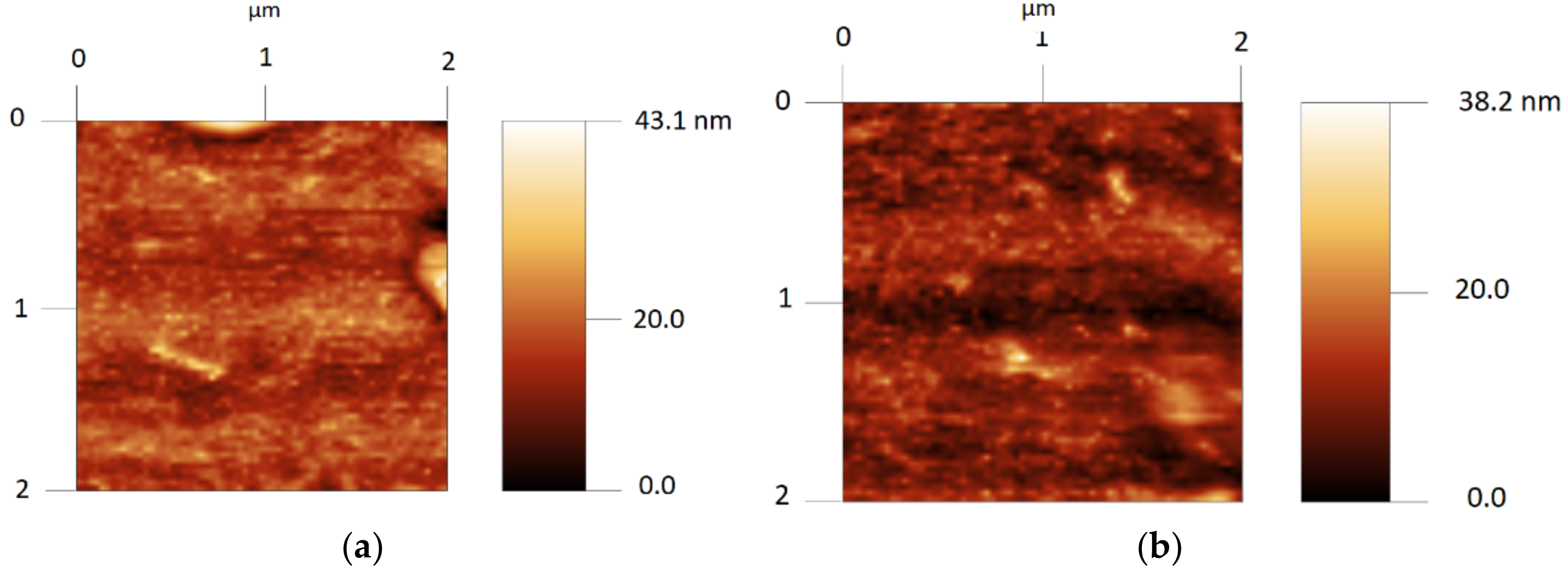
3.1. Structural Analysis

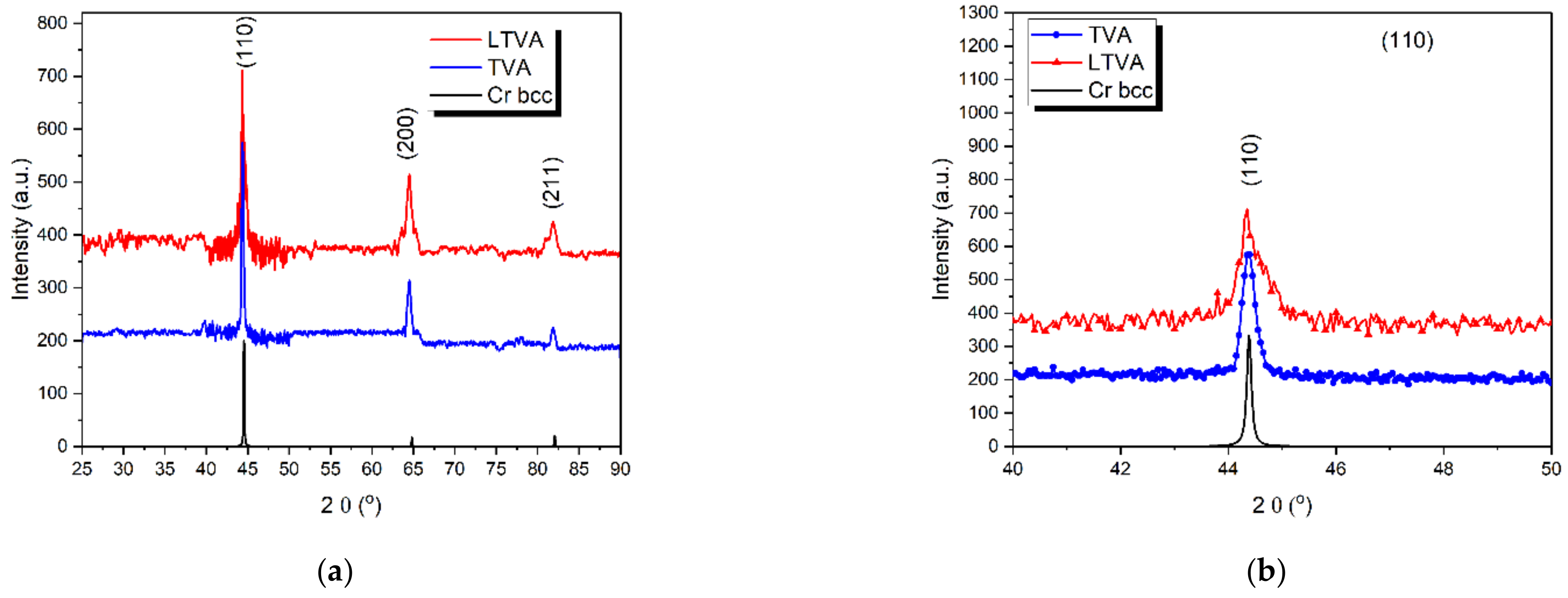
3.1.1. X-ray Diffraction

The structural analysis of the Ti:Cr thin films obtained using the TVA and LTVA methods was characterized using X-ray diffraction methods (Figure 2a). The inlet reveals the body-centered cubic structure of chromium and the (110) reflection plane.
The only peak with 2θ around 44.4° indicates a body-centered cubic bcc (110) orientation structure (Figure 2b) as indicated elsewhere [29]. The analysis of the X-ray patterns is presented in Table 2.
As can be seen, the TVA sample has a larger grain size than those from LTVA, indicating faster crystallization. Meanwhile, the titanium-doped chromium grain size from the LTVA sample has better crystalline parameters, much closer than the standard Cr monocrystals.

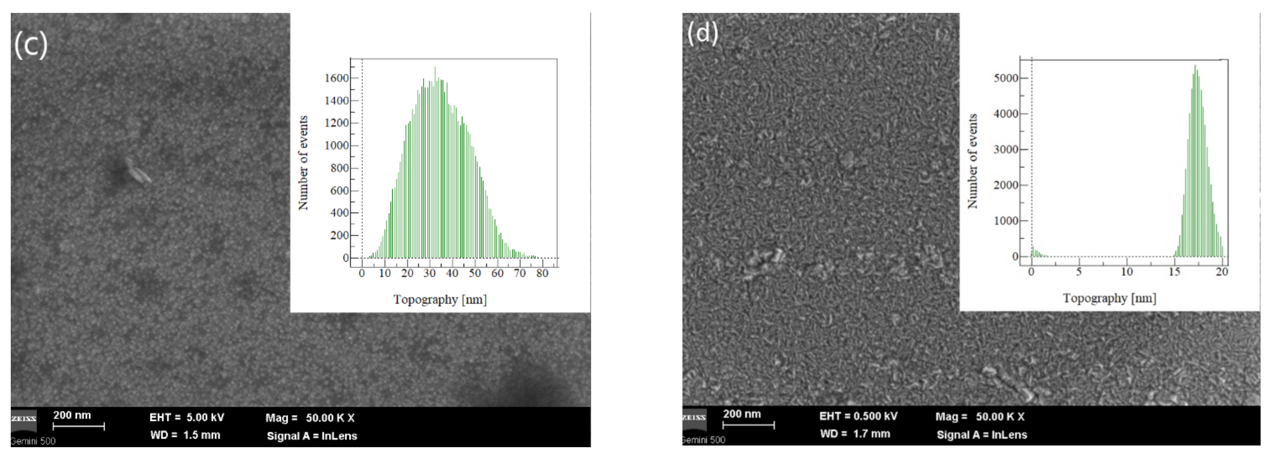
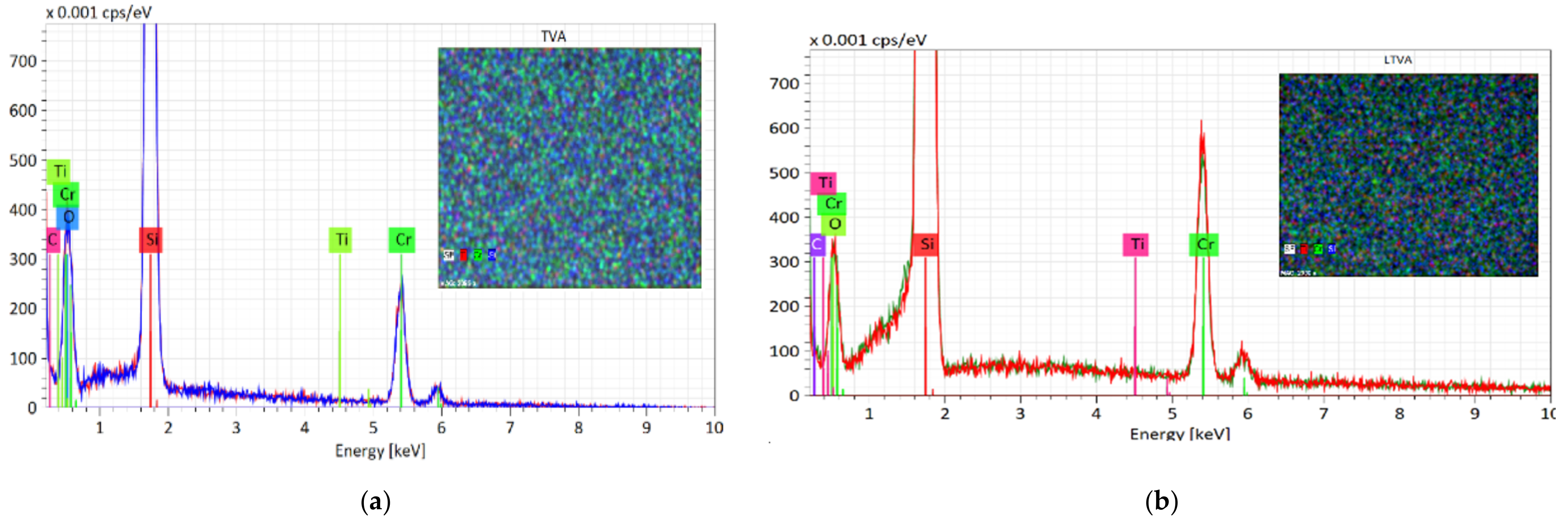
3.1.2. SEM and EDX Analysis

The scanning electron microscopy (SEM) images of the surface morphology of Ti:Cr thin films grown on a silicon substrate are shown in Figure 3a,b. The Ti:Cr thin film surface prepared using LTVA looks smooth, proving it has superior deposition characteristics compared to the TVA method. Using an electron beam voltage of 5 kV, the lower electrical conductivity of the TVA sample leads to electrical charging of the surface (blacker area on image), revealing the higher conductivity of the LTVA sample.
The surface morphology of the obtained thin films is well evidenced in the SEM images taken at lower electron beam voltage, thus avoiding the effects of surface charging (Figure 3c,d).
The SEM images show the higher roughness of the TVA sample than one of the LTVA samples. Furthermore, the 3D images present the higher roughness for the TVA sample than the LTVA sample, which shows a smoother surface. Moreover, the histogram of the roughness of the TVA sample (number of events: 0–1500) comprises a nonsymmetrical histogram centered at 33 nm with a peak height at around 1500 counts. The half-width of this Gaussian distribution is around 55 nm.
In the histogram of the LTVA sample, the nonsymmetric distribution is centered at 18 nm due to the laser beam interaction with the plasma, but their number is increased to around 5000 counts with a half-width value of 3 nm. The photonic processes induced effects that produced more nanoparticles in the LTVA sample but were more compact and uniformly distributed.
EDX analysis was performed using different electron beam acceleration voltages to decrease the substrate contribution. At low acceleration voltages, the Kα line of chromium positioned at 5,411 keV disappears, and the chromium concentration is given by the Lα line at 0.573 keV, which is very close to the Kα line of oxygen (0.525 keV) and Lα line of Ti (0.452 keV) (Figure 4a,b), resulting in a lower contribution of chromium in thin films and an artificial increase in titanium concentrations.
The estimated concentration from the EDX measurements for the Ti ions is around 2.5% from the whole Cr films for both samples; all measurements were a sum of three monitored points in each sample. Thus, the mapping chart reveals a uniform distribution of Ti and Cr on the entire surface (Figure 4a). The same is true for the Ti:Cr sample deposited using the LTVA method (Figure 4b). The atomic concentrations from the TVA and LTVA samples are presented in Table 3, calculated as a mean value between three different points on each sample.
Atomic force microscopy, recorded on 2 × 2 µm areas, confirms the results obtained using scanning electron microscopy, showing increases on the z-scale up to 43.1 nm of large particles in the TVA sample (Figure 5a) compared with those from the LTVA sample (Figure 5b), where the more uniform distribution of nanoparticles can be seen with a z-scale below 38.2 nm. The roughness of the selected areas is 40.5 nm for the TVA sample and 23.2 nm for the LTVA sample, confirming the particle distributions obtained by the SEM measurements.

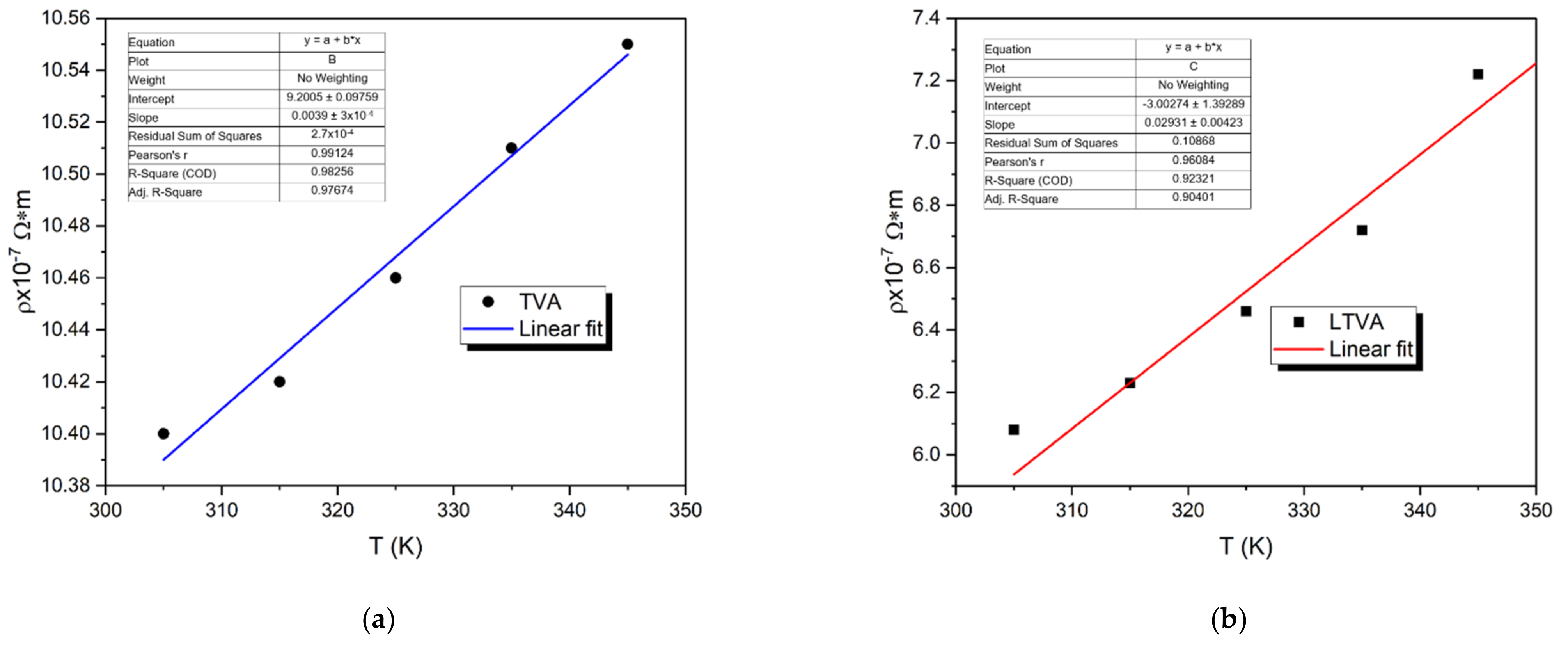
3.2. Electrical Measurements

The voltage–current curves for the TVA and LTVA samples (Figure 6a,b), which account for the voltage in the inner electrodes versus the current in the outer electrodes, reveal the lower resistivity of the LTVA samples (ρ = 6.08 × 10⁻⁷ Ω·m) compared to the TVA sample resistivity (ρ = 10.4 × 10⁻⁷ Ω·m). Both films have higher resistivity than the bulk resistivity value for the chromium element, ρ = 1.2 × 10⁻⁷ Ω·m [29].
Moreover, the resistivity versus temperature shows linear dependence up to 350 K and, based on the evaluation of the slope, the values of the temperature coefficient of resistance are α = 3.9 × 10⁻³ K−1 for the TVA sample and α = 29 × 10−3 K−1 for the LTVA sample, which is considerably higher than in the bulk chromium metal α =2.9 × 10⁻³ K−1 [30].

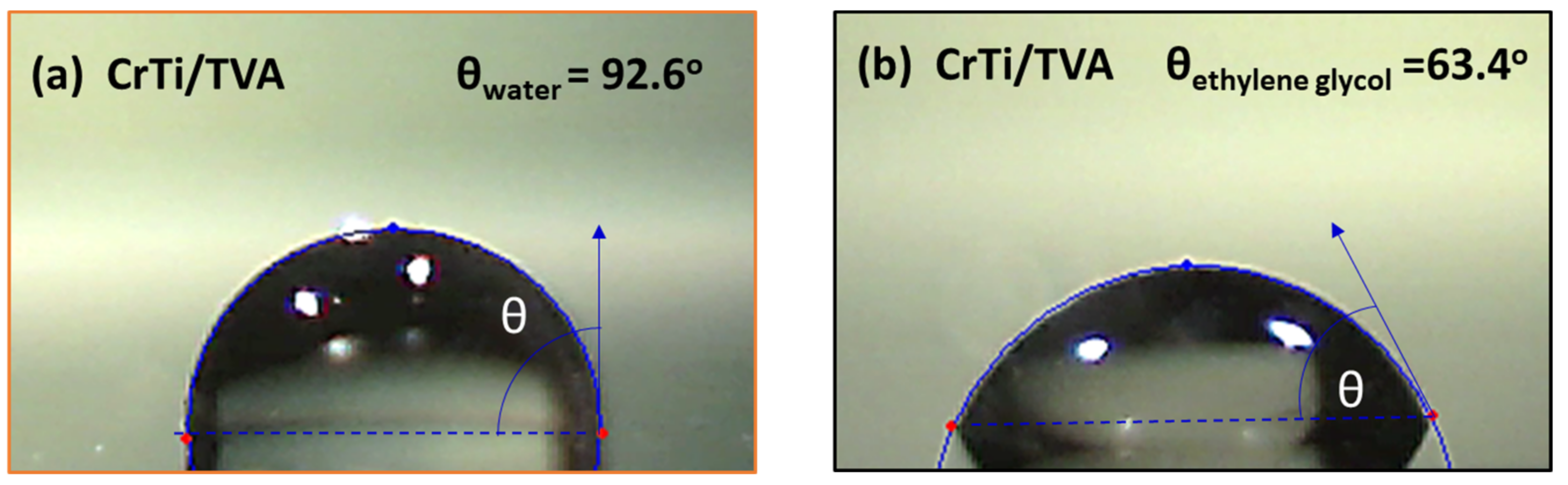
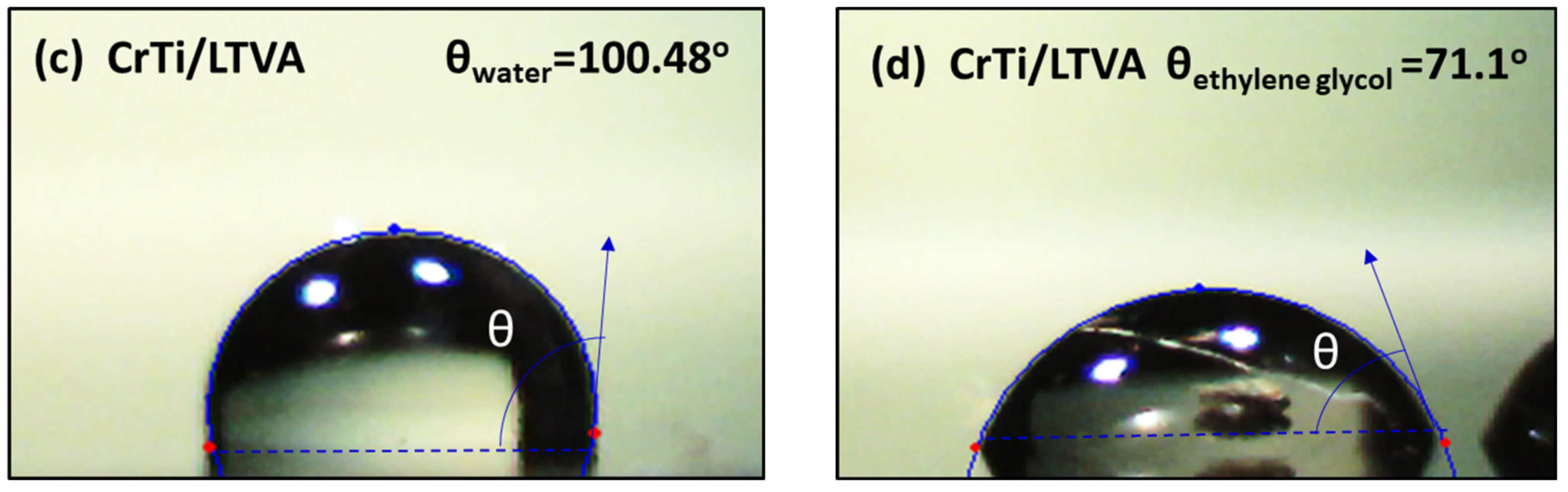
3.3. Wettability Measurements

Wettability measurements revealed the physical properties of materials related to their adhesion to the surrounding media. Such materials have high surface free energy, as a large amount of energy is released when it is dissociated into smaller pieces [31]. Wettability is related to the surface free energy involving the measurement of contact angles as the primary data, which indicates the degree of wetting when a solid and liquid interact.
Typical image frames acquired using the image analysis system described are displayed in Figure 7a–d. The figures show a printout of the side view of a sample during the experimental measurement of distilled water and ethylene glycol on the substrate. The selection of several points on the solid–liquid and liquid–vapor interface makes it possible to fit the drop profile and calculate the tangent angle of the solid surface drop. To obtain as precise results as possible, the profile of the drop was fitted with three basic points: two on the liquid-solid interface—the baseline, and one on the drop contour.
These data were digitalized and measured using the included software, and the free surface energies were further analyzed using the Owens–Wendt method. Small contact angles correspond to high surface free energy, while large contact angles correspond to low surface free energy [32]. Thus, a small contact angle (TVA) involves a high surface free energy, corresponding to the high energy dissociation of the measured thin films.
The main parameters for the two types of samples deposited on the Si wafer using different methods are summarized in Table 4.
In conclusion, from all images presented in Figure 7, the contact angle is lower for the Ti:Cr sample deposited using the TVA method for both liquids used (water and ethylene glycol) than those obtained using the LTVA method.

4. Discussion

The above results indicate the superior characteristics of the LTVA thin films compared with those obtained using the TVA method. When a high-power pulsed laser is focused onto this plasma, the flow of the photonic beam affects the photoionization processes. As a result, the collision rate increases and the energy is transferred from the excited free electrons and ions to the thin film surfaces. In fact, the increase in the photoionization processes ensures not a different deposition rate but a superior quality of the surfaces of the LTVA samples. These improvements are revealed below.
The cell parameters for both samples are refined using a body-centered cubic bcc structure as provided by the XRD database (PDF#04-001-0046) with a = b = c = 2.876 Å, α = β = γ = 90° for the TVA sample and a = b = c = 2.882 Å, α = β = γ =90° for the LTVA sample. These parameters are in good correlation with the standard crystallization of chromium bcc described by Wyckoff, being Im3m structure with a = b = c = 2.8839 Å and α = β = γ = 90° [33].
Chromium metal was found in six crystallographic forms: α-Cr, bcc, a = 2.885 Å; β-Cr, hcc, a = 2.72 Å and 4.42 Å; γ-Cr, cfc, a = 8.73 Å; ε-Cr, cfc, a = 3.86 Å; η-Cr, cfc, a = 3.80 Å; and δ-Cr, pc, a = 4.59 Å [34]. While β and ε phases were assigned to chromium hydrates, the η-Cr phase can only be obtained at high temperatures, and the δ-Cr phase is rare and dependent on some special conditions with γ-Cr and has not been observed since 1930; the most common phase remains α-Cr, which was very often observed in chromium thin films [2,35].
The grain sizes D of the Ti:Cr nanocrystals were evaluated using the known Debye–Scherrer formula:
D = K × λ β × cos θ
where K is a form factor usually taken as 0.9 for the cubic crystallographic symmetries, λ = 1.54 Å is the wavelength of the X-rays, β is the full width at half maximum (FWHM) in radians, and θ is degree. This formula assumes a strain-free sample. The β parameter was corrected to eliminate the intrinsic and instrumental broadening using the equation:
β = β m 2 β corundum 2
where βm is the half-height width of the measured sample (110) peak and βcorundum is the half-height width of the (113) peak at 43.33° of a standard corundum sample obtained experimentally. The analysis of X-ray diffraction profiles is a standard method to determine the crystallite size of nanoparticles. However, this method is affected by different factors, such as the low resolution of the X-ray diffraction setup or the peak asymmetric profile.
The roughness of the TVA sample shows two Gaussian distributions, with one centered at around 1 µm, meaning a non-uniform deposition of Ti:Cr nanoparticles, with a higher distribution centered at 145 nm but with a large distribution of 180 nm half-width. In contrast, in the LTVA, only one distribution is centered at 175 nm with a smaller half-width, suggesting a more uniform particle distribution, but much higher numbers.
The thin metal film composition mapping shows a uniform distribution of Ti in the chromium film, even at lower concentrations. These results reveal the better performance of the Ti:Cr thin films deposited using the LTVA method, including the results obtained from the XRD patterns.
The electrical properties depend on the thickness approaches, which should be compared with the electron mean free path, accounting for electron scattering with interfaces and defects [36]. Although, as the structural analysis shows, there is a difference in the sample grain sizes; the TVA sample has larger dimensions. These grain-like structures induce discontinuities, which lead to higher resistivity [37].
The LTVA sample has a higher resistivity drop due to higher phonon scattering. A small crystallinity domain, observed in the XRD measurements for grain sizes, increases the phonon scattering processes equivalent to the amorphous thin films [38]. Therefore, increasing the grain size in the TVA sample will reduce the cusped minimum equivalent with a crystallization process and increase the spin-ordering process, reducing the phonon scattering processes [9].
The value of the temperature coefficient of resistance of the Ti:Cr sample deposited using LTVA technology is one order of magnitude higher than those deposited using classical TVA, meaning that the amorphous structure has a pronounced character.
The higher surface free energy of the TVA sample suggests higher energy dissociation due to the small particle sizes but higher crystallinity. In comparison, the lower surface free energy of the Ti:Cr sample deposited using the LTVA method reveals a more amorphous structure of the thin film with a smaller crystallite embedded, which was also validated by the XRD measurements. Moreover, a higher contact angle for the LTVA confirms a smoother surface of the chromium thin film, as is shown in the SEM images.

5. Conclusions

The structural, electrical, and surface energy measurements confirm the superior characteristics of the Laser-Induced Thermionic Vacuum Arc method used for titanium-doped chromium thin films. The laser-induced TVA method does not influence the doping process with the titanium ions, but, just for a small quantity of Ti, the obtained thin films show uniform distributions. These superior characteristics of the LTVA samples are supported by: (a) the lower roughness of the samples obtained using the LTVA method revealed by the SEM images reconstructed in 3D and AFM images; (b) the lower electrical conductivity observed in the SEM images for the TVA sample, which results in a faster electron charge of their surfaces; (c) the higher conductivity of the LTVA samples; and (d) the higher contact angle for the LTVA samples, resulting in the lower free energy surface, associated with lower roughness. Moreover, the wettability measurements confirm lower dissociation energy for the LTVA samples, which emphasizes the amorphous character of the Ti-doped chromium layers.

Author Contributions

Conceptualization, R.V. and S.P.; methodology, S.P. and R.V.; software, A.M.; investigation, V.C., V.D., and E.M.; writing—original draft preparation, S.P.; writing—review and editing, R.V.; funding acquisition, R.V. and S.P. All authors have read and agreed to the published version of the manuscript.

Funding

This research was funded by JINR-UOC, grant number 04-4-1142-2021/2025 item 49 and 04-4-1143-2021/2025 item 55.

Institutional Review Board Statement

Not applicable.

Informed Consent Statement

Not applicable.

Data Availability Statement

Not applicable.

Conflicts of Interest

The authors declare no conflict of interest.

References

  1. Zarras, P.; Stenger-Smith, J.D. Smart Inorganic and Organic Pretreatment Coatings for the Inhibition of Corrosion on Metals/Alloys. Intell. Coat. Corros. Control 2015, 11, 59–91. [Google Scholar] [CrossRef]
  2. Wang, S.F.; Lin, H.C.; Bor, H.Y.; Tsai, Y.L.; Wei, C.N. Characterization of chromium thin films by sputter deposition. J. Alloy. Comp. 2011, 509, 10110–10114. [Google Scholar] [CrossRef]
  3. Delmotte, F.; Ilse, J.M.; Salmassi, F.; Soufli, R.; Burcklen, C.; Rebellato, J.; Jerome, A.; Vickridge, I.; Briand, E.; Gullikson, E. Soft X-ray optical constants of sputtered chromium thin films with improved accuracy in the L and M absorption edge regions. J. Appl. Phys. 2018, 124, 035107. [Google Scholar] [CrossRef]
  4. Martinez-Galarce, D.S.; Soufli, R.; Windt, D.L.; Bruner, M.; Gullikson, E.; Khatri, S.; Spiller, E.; Robinson, J.C.; Baker, S.; Prast, E. Multisegmented, multilayer-coated mirrors for the Solar Ultraviolet Imager. Opt. Eng. 2013, 52, 095102. [Google Scholar] [CrossRef] [Green Version]
  5. Soufli, R.; Robinson, J.C.; Fernandez-Perea, M.; Spiller, E.; Brejnholt, N.F.; Descalle, M.A.; Pivovaroff, M.J.; Gullikson, E.M. Recent advances in reflective optics for EUV/x-ray laser sources. X-ray Lasers 2014, 169, 331. [Google Scholar] [CrossRef]
  6. Graessle, D.E.; Soufli, R.; Nelson, A.J.; Evans, C.L.; Aquila, A.L.; Gullikson, E.M.; Blake, R.L.; Burek, A.J. Iridium optical constants from synchrotron reflectance measurements over 0.05 to 12 keV X-ray energies. Proc. SPIE 2004, 5538, 72–83. [Google Scholar]
  7. Shrivastava, R.; Upreti, R.K.; Seth, P.K.; Chaturvedi, U.C. Effects of chromium on the immune system. FEMS Immunol. Med. Microbiol. 2002, 34, 112. [Google Scholar] [CrossRef]
  8. Wang, G.; Long, X.; Zhang, L.; Wang, G.; Polosan, S.; Tsuboi, T. Spectroscopic characteristic and energy levels of Cr3+ in Cr3+:KAl(MoO4)2 crystal”. J. Lum. 2008, 128, 1556. [Google Scholar] [CrossRef]
  9. Marcinkowski, M.J.; Lipsitt, H.A. Electrical Resistivity of Chromium in the Vicinity of the Néel Temperature. J. Appl. Phys. 1961, 32, 1238. [Google Scholar] [CrossRef]
  10. Ferreira, A.A.; Silva, F.J.G.; Pinto, A.G.; Sousa, V.F.C. Characterization of Thin Chromium Coatings Produced by PVD Sputtering for Optical Applications. Coatings 2021, 11, 215. [Google Scholar] [CrossRef]
  11. Davis, J.R. Corrosion: Understanding the Basics; Davis, J.R., Ed.; ASM International: Materials Park, OH, USA, 2000; pp. 331–358. [Google Scholar]
  12. Korinek, K.A. Chromate conversion coatings. In ASM Handbook; Korb, L.J., Olson, D.L., Eds.; ASTM International: West Conshohocken, PA, USA, 1998; Volume 13, pp. 389–395. [Google Scholar]
  13. Angadi, M.A.; Udachan, L.A. The effect of substrate temperature on the electrical properties of thin chromium films. J. Mater. Sci. 1981, 16, 1412–1415. [Google Scholar] [CrossRef]
  14. Angadi, M.A.; Udachan, L.A. Influence of DC electric field on sheet resistance of thin tin and chromium films. J. Phys. D Appl. Phys. 1981, 14, L81. [Google Scholar] [CrossRef]
  15. Lozanova, V.; Lalova, A.; Soserov, L.; Todorov, R. Optical and electrical properties of very thin chromium films for optoelectronic devices. J. Phys. Conf. Ser. 2014, 514, 012003. [Google Scholar] [CrossRef] [Green Version]
  16. Angadi, M.A.; Udachan, L.A. The effect of the deposition rate on the electrical resistivity of thin tin films. Thin Solid Film 1981, 78, 299–302. [Google Scholar] [CrossRef]
  17. Musa, G.; Mustata, I.; Blideran, M.; Ciupina, V.; Vlădoiu, R.; Prodan, G.; Vasile, E.; Ehrich, H. Thermionic Vacuum Arc (TVA) new technique for high purity carbon thin film deposition. Acta Phys. Slovaka. 2005, 55, 417–421. [Google Scholar]
  18. Vladoiu, R.; Tichý, M.; Mandes, A.; Dinca-Balan, V.; Kudrna, P. Thermionic Vacuum Arc-A versatile technology for thin film deposition and its applications. Coatings 2020, 10, 211. [Google Scholar] [CrossRef] [Green Version]
  19. Vladoiu, R.; Ciupina, V.; Lungu, C.P.; Bursikova, V.; Musa, G. Thermionic vacuum arc (TVA) deposited tungsten thin film characterization. J. Optoel. Adv. Mater. 2006, 8, 71–73. [Google Scholar]
  20. Musa, G.; Vladoiu, R.; Ciupina, V.; Lungu, C.P.; Mustata, I.; Pat, S.; Akan, T.; Ekem, N. Characteristics of boron thin films obtained by TVA technology. J. Optoel. Adv. Mater. 2006, 8, 617–620. [Google Scholar]
  21. Vladoiu, R.; Mandes, A.; Dinca-Balan, V.; Prodan, G.; Kudrna, P.; Tichý, M. Magnesium plasma diagnostics by heated probe and characterization of the Mg thin films deposited by thermionic vacuum arc technology. Plasma Sources Sci. Technol. 2015, 24, 035008. [Google Scholar] [CrossRef]
  22. Ekem, N.; Musa, G.; Pat, S.; Balbag, Z.; Cenik, I.; Vladoiu, R. Carbon thin film deposition by Thermionic Vacuum Arc (TVA). J. Optoel. Adv. Mater. 2008, 10, 672–674. [Google Scholar]
  23. Tamer, A.; Ekem, N.; Pat, S.; Issever, U.G.; Balbag, M.Z.; Cenik, M.I.; Vladoiu, R.; Musa, G. Boron thin film deposition by using Thermionic Vacuum Arc (TVA) technology. Mater. Lett. 2007, 61, 23. [Google Scholar] [CrossRef]
  24. Vladoiu, R.; Mandes, A.; Dinca, V.; Kudrna, P.; Tichý, M.; Polosan, S. Magnesium-silver cathodes for efficient charge-injection into Organic Light Emitting Diodes deposited by LTVA method. J. Alloy. Comp. 2021, 869, 159364. [Google Scholar] [CrossRef]
  25. Rodríguez-Barrero, S.; Fernández-Larrinoa, J.; Azkona, I.; López de Lacalle, L.N.; Polvorosa, L. Enhanced Performance of Nanostructured Coatings for Drilling by Droplet Elimination. Mater. Manuf. Processes 2014, 11, 3582. [Google Scholar] [CrossRef]
  26. Fernández-Abia, A.I.; Barreiro, J.; López de Lacalle, L.N.; Martínez-Pellitero, S. Behavior of austenitic stainless steels at high speed turning using specific force coefficients. Int. J. Adv. Manuf. Technol. 2012, 62, 505. [Google Scholar] [CrossRef]
  27. Rachinger, W.A. A Correction for the α1 α2 Doublet in the Measurement of Widths of X-ray Diffraction Lines. J. Sci. Instrum. 1948, 25, 254–255. [Google Scholar] [CrossRef]
  28. Vladoiu, R.; Dinca, V.; Musa, G. Surface energy evaluation of unhydrogenated DLC thin film deposited by thermionic vacuum arc (TVA) method. Eur. Phys. J. D 2009, 54, 433–437. [Google Scholar] [CrossRef]
  29. Kasap, S.; Koughia, C.; Ruda, H.E. Electrical Conduction in Metals and Semiconductors. In Springer Handbook of Electronic and Photonic Materials; Springer: Berlin/Heidelberg, Germany, 2017. [Google Scholar] [CrossRef]
  30. Rauf, A.; Ahmed, K.; Nasim, F.; Khan, A.N.; Gul, A. Optical and structural properties of Cr and Ag thin films deposited on glass substrate. IOP Conf. Ser. Mater. Sci. Eng. 2016, 146, 012013. [Google Scholar] [CrossRef] [Green Version]
  31. Rudawska, A. Surface treatment methods. Surf. Treat. Bond. Technol. 2019, 11, 47–62. [Google Scholar] [CrossRef]
  32. Yuan, Y.; Lee, T.R. Contact Angle and Wetting Properties. In Surface Science Techniques; Bracco, G., Holst, B., Eds.; Springer Series in Surface Sciences; Springer: Berlin/Heidelberg, Germany, 2013; Volume 51, pp. 3–34. [Google Scholar] [CrossRef]
  33. Wyckoff, R.W.G. Crystal Structures, 2nd ed.; Interscience Publishers: New York, NY, USA, 1963; pp. 7–83. [Google Scholar]
  34. Gasgnier, M.; Nevot, L. Analysis and crystallographic structures of chromium thin films. Phys. Stat. Sol. 1981, 66, 525–540. [Google Scholar] [CrossRef]
  35. Kulkarni, A.K.; Chang, L.C. Electrical and structural characteristics of chromium thin films deposited on glass and alumina substrates. Thin Solid Film. 1997, 301, 17–22. [Google Scholar] [CrossRef]
  36. Fuchs, K. Electrical resistance in thin metal films. Math. Proc. Cambr. Philo. Soc. 1938, 34, 100–193. [Google Scholar] [CrossRef]
  37. Mayadas, A.F.; Shatzkes, M. Electrical-resistivity model for polycrystalline films: The case of arbitrary reflection at external surfaces. Phys. Rev. B 1970, 1, 1382–1389. [Google Scholar] [CrossRef]
  38. Suezaki, Y.; Mori, H. Dynamic Critical Phenomena in Magnetic Systems: Electrical Resistivity near the Néel Point. Prog. Theor. Phys. 1969, 41, 1177–1189. [Google Scholar] [CrossRef] [Green Version]
Figure 1. Schematic of the experimental LTVA system for TiCr thin film deposition. The photo of each plasma discharge (TVA and LTVA) captured during deposition is presented in the circle on the right side.
Coatings 12 00470 g001
Figure 2. (a) X-ray diffraction patterns of Ti-doped chromium thin films; (b) reflection on (110).
Coatings 12 00470 g002
Figure 3. SEM images and 3D surfaces of (a) TVA sample and (b) LTVA sample; (c) low-voltage SEM images and histograms of TVA sample; (d) LTVA sample.
Coatings 12 00470 g003aCoatings 12 00470 g003b
Figure 4. EDX patterns and mapping for the TVA and LTVA samples at 10 kV (a) and 20 kV (b). Inlets contain the mapping of samples.
Coatings 12 00470 g004
Figure 5. AFM images of TVA (a) and LTVA (b). The scales on the right show the maximum roughness of each sample.
Coatings 12 00470 g005
Figure 6. Resistivity versus temperature for the TVA (a) and LTVA (b) samples.
Coatings 12 00470 g006
Figure 7. Contact angle for the TVA sample measured in (a) water and (b) ethylene glycol. Contact angle for the LTVA sample measured in (c) water and (d) ethylene glycol.
Coatings 12 00470 g007aCoatings 12 00470 g007b
Table 1. The list of the experimental parameters for depositing Ti:Cr thin films.
ParametersTVALTVA
Energy/pulse of laser E (mJ)0102
Irradiance of laser IL (GW/cm2)020
Base pressure pB (Pa)4.1 × 10⁻⁵
Working pressure pw (Pa)1.5 × 10⁻⁴
Distance dA-C (m)5 × 10⁻³
Distance dA-S (m)6 × 10⁻²
Intensity current on the filament IF (A)57
Input arc power P (W)460
Film thickness t (nm)100
Time of deposition Tdep (s)210
Table 2. Experimental parameters from XRD measurements.
SamplePeak (°)hklPeak Widthd-SpacingD (nm)
TVA44.3793(110)0.34202.039525
LTVA44.4243(110)0.77592.037611
Table 3. The atomic concentrations from the TVA and LTVA samples.
SampleElementSeriesAtomic NumberAtomic Conc. %Errors %
TVASiK-series1492.343.2
TiK-series220.190.0
CrK-series247.470.4
LTVASiK-series1493.153.3
TiK-series220.190.0
CrK-series246.660.3
Table 4. Contact angles and free surface energy for TiCr samples deposited by TVA and LTVA.
Sample Ti:Cr/SiContact Angle θ (°)Owens–Wendt (mJ/m2)
WaterEthylene Glycol
TVA92.6763.4029.01
LTVA100.4871.2321.58
Publisher’s Note: MDPI stays neutral with regard to jurisdictional claims in published maps and institutional affiliations.

