
Highly Coercive L10-Phase Dots Obtained through Low Temperature Annealing for Nano-Logic Magnetic Structures


National Institute for Materials Physics, P.O. Box MG-7, Magurele, 077125 Bucharest, Romania
*
Author to whom correspondence should be addressed.
Coatings 2023, 13(12), 2068; https://doi.org/10.3390/coatings13122068
Submission received: 17 November 2023
/
Revised: 5 December 2023
/
Accepted: 9 December 2023
/
Published: 11 December 2023
(This article belongs to the Special Issue Advances of Nanoparticles and Thin Films)
Abstract
:Nano-logic magnetic structures are of great interest for spintronic applications. While the methods used for developing arrays of magnetic L10-phase dots are, in most cases, based on deposition followed by annealing at high temperatures, usually around 700 °C, we demonstrate here a technique where a much lower annealing temperature (i.e., 400 °C) is needed in order to promote fully the disorder–order phase transformation and achievement of highly coercive L10-phase dots. In order to develop building blocks based on arrays of L10-phase FePt dots for further spintronic applications, an engraving technique using electron beam lithography is employed. This paper describes the fabrication, as well as the morphological and magnetic characterization, of regularly placed FePt dots of various shapes, as pre-requisites for integration into nano-logic devices. As a proof of concept, regular arrays of FePt circular dots were devised and their structural characterization, using X-ray diffraction (XRD) and transmission electron microscopy (TEM), was performed. It has been shown that annealing at only 400 °C for 30 min proved the occurrence of the tetragonal L10 phase. Moreover, structural characterization showed that the disorder–order phase transformation was complete with only the L10 phase detected in high resolution TEM. The magnetic characterization provided more insight into the potential of such arrays of magnetic devices with convenient values of magnetic coercivity, remanent and saturation magnetization. These findings show good potential for developing regular arrays of uniformly shaped magnetic entities with encouraging magnetic performances in view of various applications.
1. Introduction
There has been a surge of interest in the investigation of size-dependent phenomena as a response to the industry needs for highly performant nanodevices. The recent award of the Nobel Prize in Chemistry 2023 to the pioneers of the development of quantum dots fabrication [1] shows how important and necessary is the study of size-dependent phenomena at nanoscale. A special case is of the nanoscale-structured thin films and coatings. Of particular interest is the magnetic dots or nanostructures that are suitable for spintronic applications as well as for heated-dot magnetic recording (HDMR). The formation of hybrid nanostructures in spintronic devices has been recently investigated [2] as a response to specific needs, especially in nanodiagnostics, nanoelectronics and adjacent fields, where combined optical and magnetic responses to various excitations is required for various types of sensing. With the advent of high-accuracy and high-resolution fabrication technologies, such as lithography, coupling phenomena at the nanoscale in magnetic dots and in arrays of dots may become accessible. The integration of magnetic and semiconductor components adds new capabilities to electronic devices [3]. While spin phenomena have long been investigated within the context of conventional ferromagnetic materials, the study of spin generation, relaxation and spin-orbit coupling in non-magnetic materials has taken off only recently with the advent of hybrid spintronics. Therefore, many novel materials and associated nanoarchitectures can find their greatest potential in both science and technology. On the other hand, the heated-dot magnetic recording (HDMR) principle, derived from the heat-assisted magnetic recording (HAMR), was shown to be a targeted application where a key system is represented by FePt nanoclusters [4,5]. In this view, Mohan et al. [4] and Medwal et al. [5] have proposed the fabrication of self-stabilized FePt non-stoichiometric clusters by a chemical route, i.e., reduction using oleic acid and oleylamine. An annealing at 600 °C transformed these FePt colloidal nanoparticles into carbon-coated L10 FePt-phase nanoclusters. As proposed by Seagate a few years ago [6], the heated dot magnetic recording (HDMR) is a promising technology suitable for increasing the density of media used for magnetic recording to values around 4 Tb/in2. It is indeed true that the heated-dot magnetic recording technology needs arrays of magnetic dots, periodically dispersed, non-interacting and well within the nanometer-size range, with stable magnetic response and high uniaxial perpendicular magnetic anisotropy. While the chemical route described in [4,5] provides non-interacting, small nanoparticles, their carbonaceous coating can impede the recording processes by diminishing the magnetic response. The lithographical route proposed in [6] has the advantage of providing regular disposal of these small nanoclusters. Here, the media is made of a continuously deposited FePt film and a lithographical path is employed to provide and define regular arrays of periodically disposed magnetic dot, which are subsequently heated to achieve the L10 FePt phase.
A systematic study on the size dependence of the coercivity in FePt magnetic dots has been developed in [7,8]. In these works, FePt nanodot arrays were fabricated by film pattering via electron beam lithography followed by ion etching. Their magnetic properties were investigated using the technique of X-ray magnetic circular dichroism combined with magneto-optic Kerr effect (MOKE) magnetometry. It was shown that circular magnetic dots with thickness of 6 nm and sizes between 30 and 100 nm exhibit a coercivity increase at decreasing sizes upon annealing at quite high temperatures [8]. However, it was found that not all of the dots were achieving the L10 FePt phase and, in addition, defects at the damaged edges may drastically influence the magnetic properties.
At variance to the above-mentioned fabrication route, the initial pre-pattering of a photoresist with the subsequent deposition and processing of the magnetic material is also a reliable solution, developed especially for biosensing applications. In this respect, integrated platforms and arrays of sensors where the detection is guided by magneto-transport phenomena are used, without the need for perpendicular anisotropy in the ferromagnetic layers. For instance, pre-patterned media was used for proving the efficiency of giant magnetoresistance (GMR) spin valve sensors designed for the detection of superparamagnetic nanoparticles as potential biomolecular labels in magnetic biodetection technology [9]. In this example, a patterned self-assembly method, involving a polymer-mediated process via e-beam lithography, was used. Other applications of integrated magnetic/spintronic device microarrays in biomedical research are reported in [10,11,12].
Due to the possibilities for the manipulation of spin configuration in magnetic dots fabricated by nanolithography, there is a high potential for making nanodevices an alternative to the presently employed sensors, but ones that are more sensitive and with lower power and lower costs [11].
A lot of the recent studies of FePt nanodots report on other various issues and the applications of such systems. For instance, in [13], the FePt magnetic dots were considered in the case of heated-dot magnetic recording (HDMR) applications. Moreover, some coercivity enhancement was recently reported in the P-doped FePt prepared by electrodeposition and subsequent annealing [14]. In another simulation study, the L10 FePt dots were investigated for their potential applicability in bit patterned media [15].
The current paper describes the fabrication and morpho-structural and magnetic characterization of arrays of magnetic dots of various shapes, made of non-stoichiometric L10 FePt, as building blocks to be further used as integration platforms for nano-logic devices. Such devices with various shapes and geometries and with convenient magnetic responses are suitable for both bio-sensing and potentially for HDMR applications. The pre-patterning route of a photoresist followed by the deposition of the metallic layers was found to be very suitable for a subsequent thermal treatment at a relatively low temperature. Given the expected influence of the damaged edges of the dots on the magnetic properties, the specific parameters of the engraving process were also investigated.
2. Materials and Methods
2.1. Method of Pre-Patterning and Magnetic Elements Nanofabrication
The building block needed for the integration platform was made by using electron beam lithography. The specific steps involved in the engraving technique are the standard ones. They are based on an e-beam exposure of a resist layer deposited onto the desired substrate. The e-beam lithography system uses hardware typical for the scanning electron microscopy for precise guiding of an electron beam, of nanometer size, onto the substrate, so as to form a latent image in the resist layer. The consequence of the exposure is to render the resist either more soluble (positive tone resist) or less soluble (negative tone resist) in the developer solution. The resulting pattern is furthermore transferred via etching or by depositing other materials on top of the remaining pattern. By iterating a number of steps of this type, complex structures of very short length scales can be built up. The envisaged nanostructures were fabricated in the dedicated class 1000 cleanroom. The fabrication tool used was a Raith150-Two high resolution e-beam lithography machine, dotted with Wet Etch cabinets for acids and bases/solvents, photolithography cabinet with PC-controlled spinner and hot plates, a mask aligner EVG 620 NT and a scanning electron microscopy SEM Hitachi S3400 with laser interferometer positioning stage from Raith (Raith GmbH, Dortmund, Germany). In order to obtain magnetic nanostructures with specific shapes and geometries, we considered the electron beam lithography technique. For this purpose, two photoresist layers were applied to a Si(111) substrate with a native SiO2 layer on top, i.e., methyl methacrylate (MMA EL10) and poly-methyl methacrylate (PMMA A3). Each layer was deposited via spin-coating for 60 s, at a speed of 4000 rpm and acceleration of 500 rpm/s. After the deposition of each layer, the sample was heated at 175 °C for 10 s in order to evaporate the solvent. Nanofabrication of the magnetic element was considered, in the first instance, in engraving high aspect ratio wires and, secondly, in engraving the desired shapes in the photoresist, followed by the deposition of metallic layers. The engraving was realized via electron beam lithography using a current of 15 pA. The size of the electron beam was 2 nm, whereas the field magnification was 800×. It is known that in electron beam lithography, the resist performance in terms of exposure dose latitude, sensitivity, contrast, roughness and resolution are influenced by the nature of the resist, the developer type and composition and the development technique. In our case, the dose was incremented with 0.1 μC/cm2 starting from 0.6 μC/cm2 and ending at 0.79 μC/cm2. The development was realized keeping the sample in a solution of methyl isobutyl ketone (MiBK) and isopropyl alcohol (IPA) (1:3) for 8 s and then in IPA for 1 min. Finally, the sample was dried with nitrogen gas flow. After the development, the reactive ion etching technique was implemented in order to produce a better definition of the patterned shapes. A 10 s reactive ion etching process was realized in the dedicated UHV chamber at a pressure of 15 mbar.
A layer of Pt with 30 nm thickness was deposited over the engraved desired shapes, seconded by a layer of Fe with 40 nm thickness. The deposition rate in the case of Pt was 0.25 nm/s, whereas the value corresponding to Fe deposition was 0.19 nm/s. The working pressure inside the deposition chamber was 10−7 mbar. The lift-off process was realized by placing the sample in acetone for 2 min at 50 °C and, afterwards, in acetone at room temperature for 30 min. After the removal of the photoresist, the nanostructure was furthermore annealed at 400 °C for 30 min in order to promote the atomic inter-diffusion and the formation of the L10 FePt phase.
2.2. Characterization Methods
Several investigation techniques were then used to study the structural and morphological aspects of dots as well as the phase evolution with the annealing temperature. Also, a thorough study of magnetic properties in various stages of annealing as a function of applied field or as a function of temperature were performed. The morpho-structural studies were performed via X-ray diffraction (XRD), scanning electron microscopy (SEM) and high-resolution transmission electron microscopy (HRTEM) coupled with selected area electron diffraction (SAED). For XRD, a Bruker D8 Advance (Bruker AXS GmbH, Karlsruhe, Germany) with Cu Kα radiation wavelength of 1.54 Å was used. For the SEM imaging, Lyra 3XMU with Focused Ion Beam SEM-FIB sample preparation stage, from Tescan (Tescan France, Fuveau, France), was used. The facility is equipped with secondary electron detectors with a resolution of 5 nm at 30 kV. Transmission electron microscopy in high resolution mode was recorded using a JEM ARM 200 F electron microscope operated at 200 kV acceleration voltage, from JEOL (JEOL Ltd., Hertfordshire, UK). The magnetic characterization was performed via a SQUID (Superconducting QUantum Interference Device) unit of a MPMS (Magnetic Properties Measurement System) from Quantum Design (Quantum Design Europe GmbH, Darmstadt, Germany), under magnetic applied fields of up to 12 Tesla. The measurements were taken both in parallel and perpendicular geometry and at temperatures ranging from 5 K to 300 K. The parallel and perpendicular refers to the direction of the applied magnetic field with respect to the array plane.
3. Results and Discussion
3.1. Complex Morphology Analysis
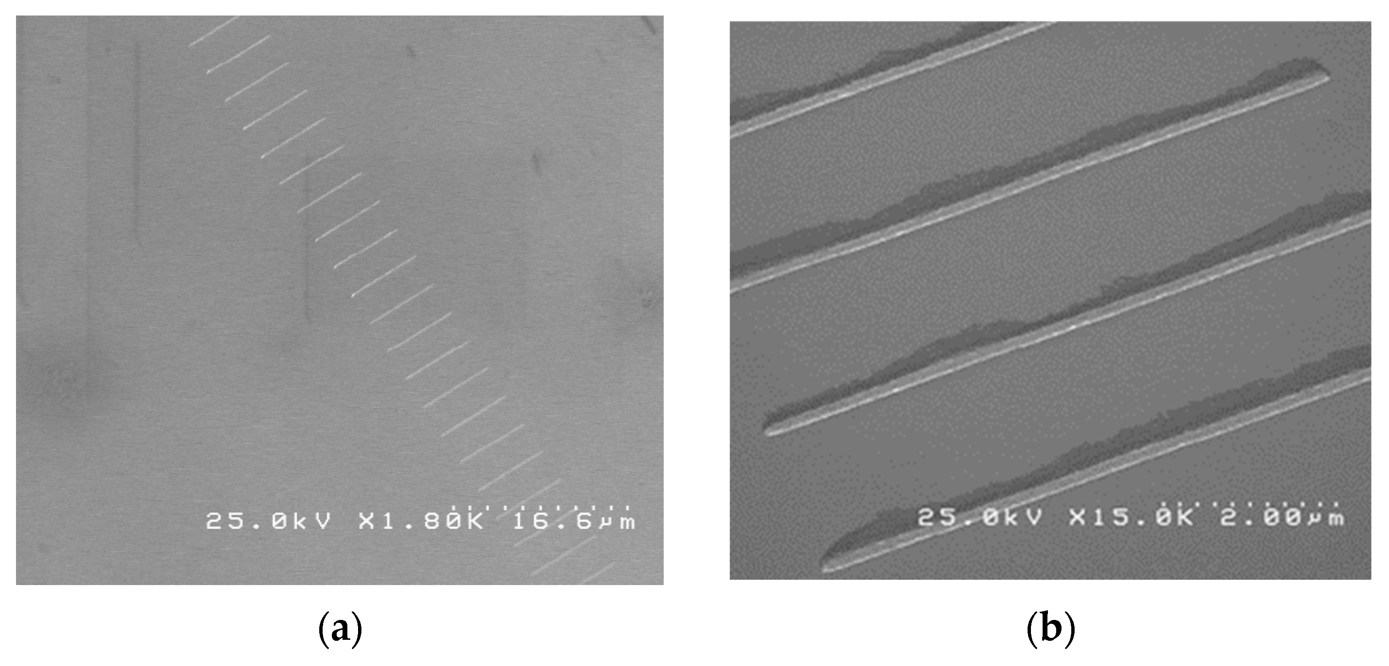
Scanning electron microscopy (SEM) images of the obtained engraved hallow nanostructures have been collected. The first set of engraved wires, with a depth of approximately 200 nm, have been obtained in a sequence of exposure doses ranging from 0.60 μC/cm2 up to 0.79 μC/cm2. The SEM image presented in Figure 1a exhibits these traits in which the doses are increasing from the top of the image to the bottom. The best formed trait, shaped as rectangle with an optimal aspect ratio, was found to occur for an exposure dose of about 0.67 μC/cm2. A second set of engraved wires, with a depth of 100 nm obtained under exposed doses ranging from 0.76 to 0.79 μC/cm2, are shown in Figure 1b.
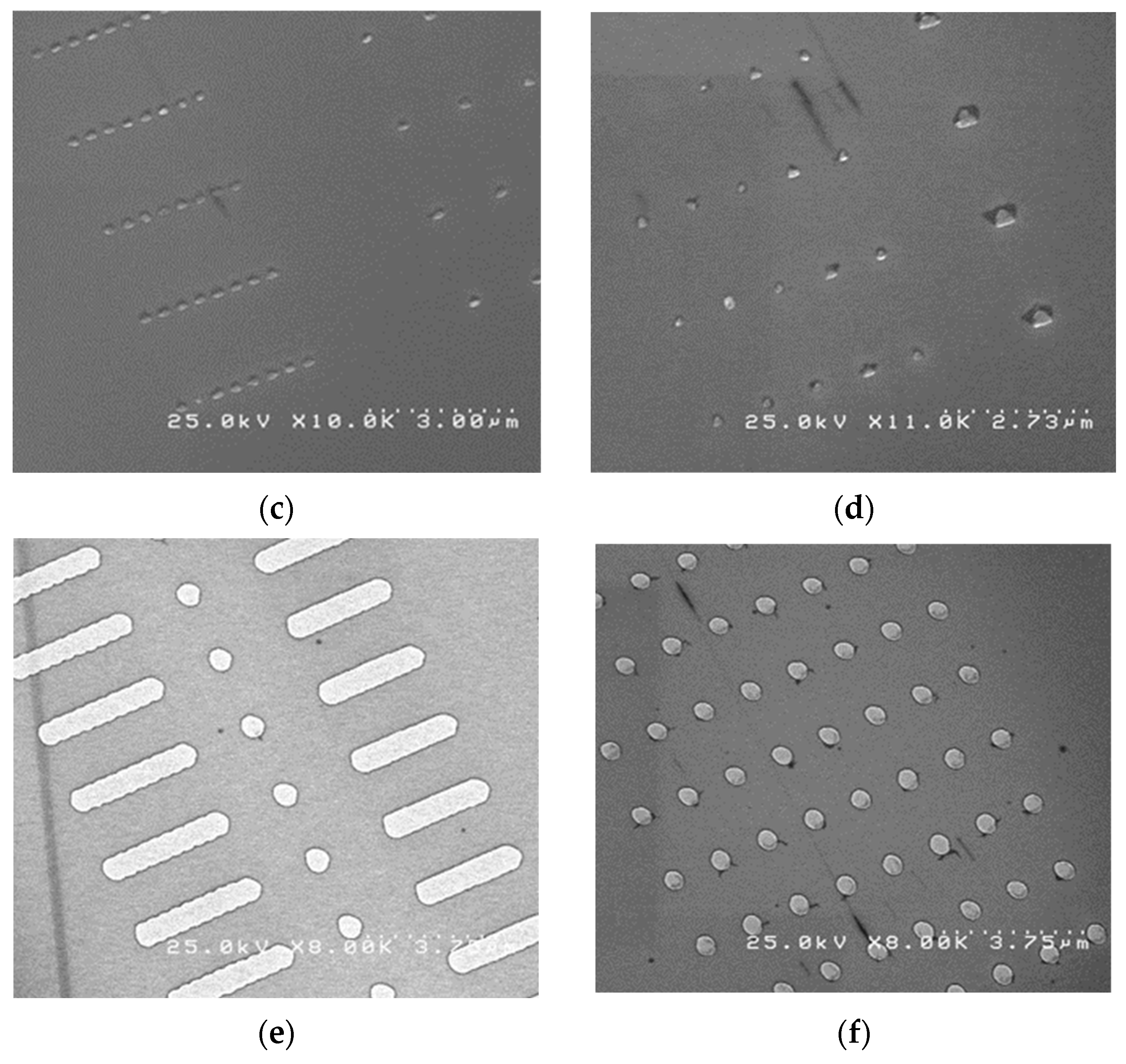
In order to obtain regular shapes of various types of magnetic structures (rectangles, triangles and circular) using electron beam lithography, reactive ion etching was implemented to improve the definition of the patterned hallow shapes. The considered hallow structures engraved on photoresist films of 200 nm thickness consist of circular structures with diameters of 200 nm with different spacing (Figure 1c), equilateral triangles with characteristic lengths of 200 nm and 400 nm, respectively (Figure 1d), and simple circular structures with diameters of 335 nm as well as rectangular structures formed by overlapping the circular structures on the y direction over 200 nm (Figure 1e). The photoresist application, the metal deposition on the hallow structures and the lift-off procedures were similar across all the deposited samples. For each hallow shape, different dose values were considered from 0.6 μC/cm2 to 0.79 μC/cm2, with 0.1 μC/cm2 discretization.
Finally, Figure 1e shows a regular array of FePt circular dots obtained after the lift-off process following the growth of the successive Pt and Fe layers according to the previous section, on the array of engraved circular structures with diameters of 335 nm.
We have further chosen these regular arrays of FePt circular magnetic dots, for structural and magnetic characterization, considering the potential of such nanostructures to be developed into an array of nanodevices, individually addressable. The same annealing treatment was applied for the considered magnetic nanostructures in order to induce the L10 FePt phase of high coercivity. The influence of the dose value during the engraving process on the phase formation was also investigated.
The creation of a wide area of magnetic dots or nanostructures, regularly dispersed and integrated onto functionalized substrates with logic capabilities, would allow for the fabrication of complex architecture structures where the magnitude and direction of magnetic moments may be individually addressed and exploited for applications in the fields of magnetic nanosensors and molecular detection.
Systems exhibiting giant magnetoresistive effect (GMR) materials are generally made of conductive regions, alternated with or separated by magnetic regions [16,17]. In a trilayer-like GMR system, a conductive layer is sandwiched between two ferromagnetic layers of different magnetization reversal mechanisms. A spin reconfiguration in the ferromagnetic layers due to the application of a magnetic field causes the spin-dependent scattering of conduction electrons moving through the nm thick conductive layer. That means the resistance of the conductive film in the trilayer spin valve system switches from a low value in cases of parallel spin configuration in the two neighboring ferromagnetic layers to a higher value in cases of an antiparallel spin configuration in the two ferromagnetic layers. Usually, the different magnetic reversal in the two ferromagnetic layers can be induced by pinning one of the layers to an antiferromagnetic one, with the generation of a unidirectional anisotropy and an exchange bias effect at the level of the pinned layer. Alternatively, one of the layers could have a much higher coercive field than of the second layer with soft magnetic properties (low coercive field) [18]. The presence of a small external magnetic field will easily change the magnetic configuration of the soft magnetic layer and, so, it can be easily detected by the changes in the resistivity of the spin valve system. This change in resistivity will be induced either in the case of in plane or out of plane anisotropy of the low coercive free and the high coercive pinned layers, the only condition being to have the driving field coplanar with the anisotropy axis in the layers. In this respect, the L10-phase of FePt films of high coercivity can be successfully used in spin valve systems, with either perpendicular anisotropy, usually requested by the magnetic recording elements, or in-plane anisotropy, requested for other types of applications (bio-medical, displacement or angular sensors). However, magnetic anisotropy can be changed from in plane to perpendicular to the plane by tuning the thickness of the FePt layers or the specific preparation conditions. In addition, it was shown in [19] that in the case of in-plane anisotropy of the free soft magnetic layer of an exchange bias spin valve structure, its hysteretic opening can be drastically diminished if the anisotropy direction of the free layer can be oriented perpendicularly to the pinning direction. This adjustment can be achieved by a so-called biasing process through a patterned hard magnetic layer next to the spin valve structure. Although Nd-Fe-B biasing layers are actually used in this respect, FePt biasing layers can be proposed in the future due to their much higher corrosion resistance, within the condition of competitive production costs.
3.2. Structural Analysis of the Regular Arrays of Magnetic Structures
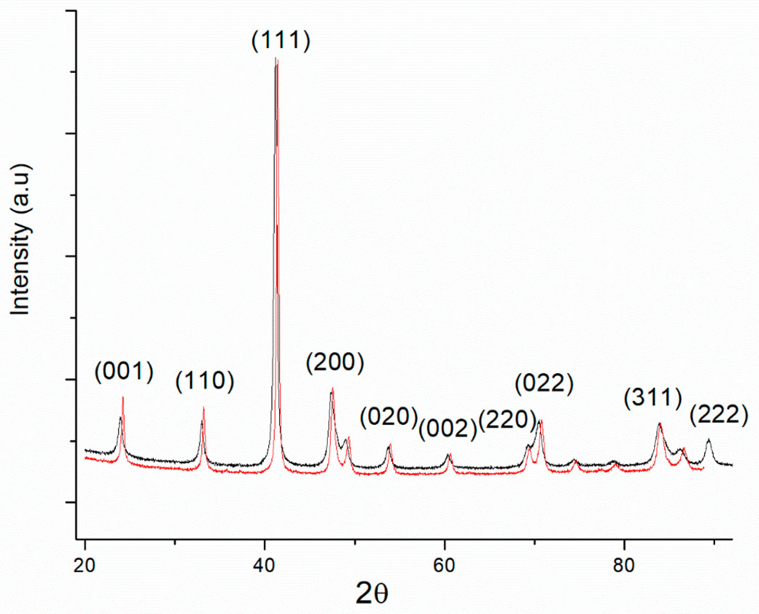
The regular arrays of magnetic dots, periodically dispersed, that are imaged in Figure 1f have been structurally investigated by means of X-ray diffraction, in a grazing incidence geometry. Such grazing geometry of the X-ray beam incidence has been carefully chosen, with an angle of 0.8 up to 1.5 degrees, in such a manner as to minimize the effect and influence of the substrate contribution into the overall patterns. The diffractograms have been recorded between 20 and 95 degrees in 2 theta. For better clarity of the structure of the regular arrays, the diffractogram of the pristine substrate in the absence of the engraved regular arrays was also recorded and subsequently subtracted from the diffractogram of the investigated samples, the difference being normalized afterwards for a better clarity. We have thus obtained a clear X-ray spectrum, consisting of diffracted beams originating only from the regular array of FePt circular dots. It is known that, usually, the bulk FePt binary alloy, either equiatomic or off-stoichiometric, is formed in a disordered A1-type cubic structure and, upon annealing, it undergoes a structural disorder–order phase transformation. Following such a transformation, the FePt would exhibit the ordered, tetragonal L10 FePt phase, which is the phase responsible for the hard magnetic properties of the system.
In Figure 2 are depicted the XRD patterns corresponding to the circular FePt dots obtained via exposure doses of 0.6 μC/cm2 and at 0.79 μC/cm2, respectively, the growth of Pt (30 nm thickness) and Fe (40 nm thickness) films, the lift-off process and subsequent annealing at 400 °C for 30 min. All the main Bragg lines of tetragonal L10 FePt are observed in both samples.
There is a strong presence of the superlattice peaks: (001) and (110) diffraction lines, as well as the presence of the main (111) Bragg lines followed by other superlattice peaks: distinctly split (200) fundamental reflection, recorded at around 48–49 degrees in 2 theta. It has to be mentioned that the two main superlattice peaks of tetragonal L10, the (001) and (110) reflections, occurs for the Cu Kα radiation we used at about 23° and 32°, respectively.
It also has to be mentioned that the main six Bragg lines of the tetragonal FePt, from lower to higher angles, are, in order, attributed to (001), (110), (111), (200), (020), (002), (220), (022), (311) and (222) hkl planes reflections. The peak assignation has been performed in agreement with the ICSD card 03-065-9121. The L10 phase lattice parameters, calculated from the full-profile analysis were found to be a = 0.384(3) nm and c = 0.317(5) nm, with an ordering parameter c/a = 0.825. In addition to the occurrence of the superlattice peaks (001) and (110) another distinct signature of the occurrence of the tetragonal L10 phase is the fact that the (200), (220) and (311) peaks are split into two. Such a feature has been encountered in other works on FePt [20,21,22] and has been unambiguously regarded as further proof of the occurrence of the L10 phase, this being due to the tetragonally distorted planes, giving rise to the spectral splitting observed in these peaks. Upon the fitting of the XRD spectra, we have also derived the average crystallite size of the L10 FePt. It has been thus observed that the average grain size of the tetragonal L10 phase increases with the exposure dose from 20 nm (for engraving with a dose of 0.6 μC/cm2) to 24 nm (for engraving with a dose of 0.79 μC/cm2). We conclude that in these XRD results, only the L10 phase has been identified. In relation to previous studies [7,8], where it has been shown that not all the FePt dots were transformed from a cubic A1 to tetragonal L10 structure, which was detrimental to the magnetic anisotropy, in our case, all the observed dots seemed to be in their ordered L10 tetragonal crystal structure.
3.3. High-Resolution Transmission Electron Microscopy and Electron Diffraction Results
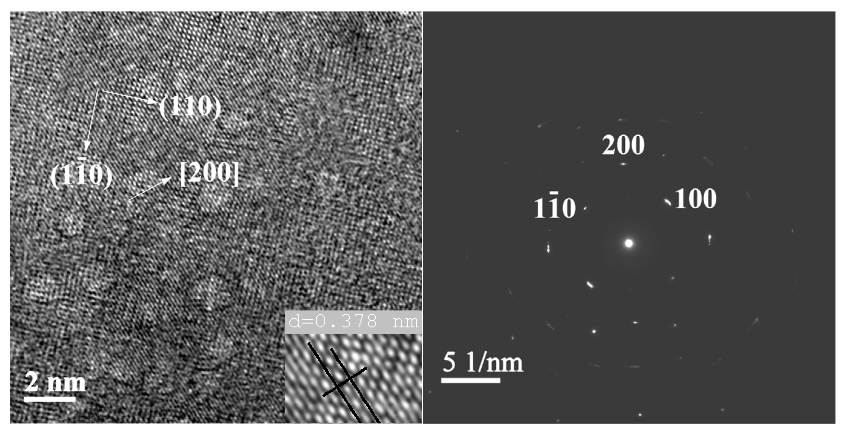
The microstructure of the granular regions on the magnetic dots’ surfaces, in the sample presented in Figure 1f, has been imaged with the help of the transmission electron microscopy in the high-resolution mode, coupled with the observation of the electron diffraction patterns, within the imaged areas on the dot surface. In the imaging area, the sample has been thinned down by ion etching of the substrate with the focused ion beam module of the microscope. A typical magnified image obtained in HRTEM is shown in Figure 3, on the left side. The high-resolution image, recorded in phase contrast imaging mode, reveals small nanocrystals of ordered tetragonal L10 FePt symmetry. The observed microstructure is apparently made of ordered FePt crystallites having a size between 4 and 8 nm, approximately, which are distributed within a wide area between 13 and 18 nm. The reticular interplanar distances, clearly observed and measured on the image, are proving the occurrence of the (110) and (1-10) superlattice reflections, which are indeed typical for the tetragonal L10 FePt phase. This confirms well, in a more illustrative way, the findings obtained from the XRD analysis, detailed above. Another main Bragg reflection of the L10 phase, the (200) reflection, is also observed and accurately measured on the image through the measuring of the interplanar distance. Taking into account that the limiting critical size for single-magnetic domains is 55 nm for L10 FePt nanograins [23], it can safely be concluded that the FePt crystallites are magnetically single domains, irrespective of their crystal symmetry or of their degree of crystallographic ordering. On the right side of the image of Figure 3, the selected area electron diffraction (SAED) image is depicted, corresponding to the area that is imaged in real space in Figure 3, on the left side. Being essentially a map of the reciprocal space, the SAED image illustrates via the brightness of the observed spots, the intensity of the corresponding planar reflection, indicating thus quantitatively the abundance of the ordered FePt grains. It is seen that SAED analysis also confirms the occurrence of the ordered L10 FePt phase in the imaged magnetic dot. The presence of the main superlattice spots, the (001) and (110) Bragg reflections of the L10 phase, in the SAED patterns, proves the occurrence of both crystallographic orientations, with the tetragonal c-axis perpendicular and parallel to the surface normal. Here, the atomic planes of a (110) nature are seen, which again confirms the occurrence of the superlattice reflections.
It is to be noted though that while Figure 3 is only an illustrative example, several other high-resolution images have been recorded, and nanocrystals of a tetragonal symmetry with detectable (001) planes, with a reticular distance of d001 = 3.78 Å, are observed in many other imaged areas, thus confirming the extended L10 ordering alongside the magnetic dot surface. It has been explained before that two crystallograhic variants are retrieved, one having the c-axis in plane and the other one having the c-axis in an orientation normal to the observing plane. Another (001) superlattice reflection, with a reticular distance of d001 = 3.67 Å, is also identified in various other imaged areas. All the c lattice parameter values measured in the observed nanocrystals with tetragonal symmetry are in good agreement with the XRD results. In the same image, a second superlattice spot attributed to the (110) Bragg reflection is observed, with a reticular distance d110 = 1.91 Å.
All the structural data are thus consistent with each other and are unambiguously proving the formation of the highly ordered L10 FePt, of tetragonal symmetry in the analyzed samples.
3.4. Magnetic Investigations of the Regular Arrays of Magnetic Nanostructures
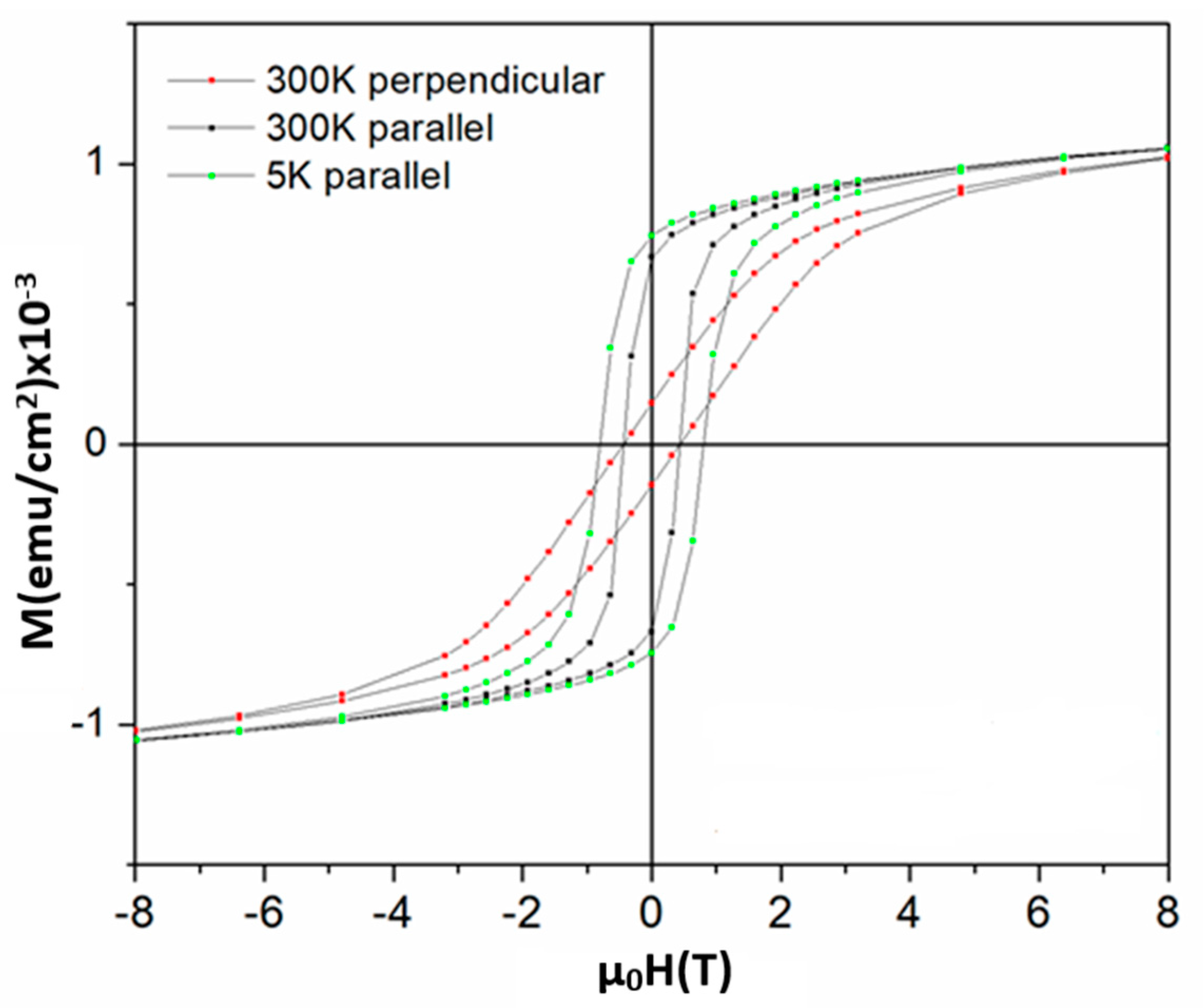
In order to assess the magnetic performances of the arrays, an investigation using the Physical Property Measurement System (PPMS) was undertaken. Magnetic hysteresis loops were measured both at 5K and at 300K in parallel and perpendicular orientation, in an applied field of up to 12 Tesla. Figure 4 depicts the magnetization reversal behavior of the regular array of FePt circular dots, namely the sample imaged in Figure 1f.
As mentioned before, the diffraction measurements did not provide any significant structural differences between samples with various exposure rates of the engraving. Only a slightly larger size of the L10 FePt crystallites at increasing doses could be mentioned, with no direct influence on the magnetic reversal. In this respect, we have chosen to show only the sample engraved with the maximum exposure rate of 0.79 μC/cm2. Notably, the sample engraved at 0.6 μC/cm2 had shown quite similar magnetic reversal, proving that the involved change in the engraving rate does not change the damaging of the dot edges.
The shape of the hysteresis loops is compatible with the presence of the L10 FePt phase, exhibiting increased saturation magnetization, remanent magnetization and magnetic coercivity. Due to the distance between the dots, their magnetic interaction should be neglected and the hysteresis loop should reflect an average of the magnetization reversal of each individual dot.
The magnetic hysteresis loops, recorded both in perpendicular and parallel geometry, do not show shoulders on the demagnetization curve. This indicates, on one side, the monophased magnetic character of the sample and, on the other side, it assures a full exchange coupling between FePt nanograins across all the investigated arrays. This is in agreement with the observed microstructure, composed of hard L10 binary FePt.
Another important observation is the fact that, at 300K, there are strong differences between the shape of the hysteresis loops recorded in parallel and in perpendicular geometry. The elongated shape of the loop in perpendicular geometry, as opposed to the rectangular shape in the case of the loop in parallel geometry, witness a pronounced in-plane magnetocrystalline anisotropy. Indeed, it was shown that such nano-islands of FePt can exhibit a strong magnetocrystalline anisotropy of about 7 × 10⁶ J/m3 [24] which should be correlated to a high coercive field along the in-plane magnetic easy axes. It was shown in [18,25] that in the case of no superposition between the coercive or switching field of the magnetization reversal along an easy axis and the saturation field of the magnetization reversal perpendicular to the easy axis, the magnetization reversal mechanism occurs through nucleation and movements of magnetic domains. In the present case, the coercive field measured in parallel geometry at 300 and 5K is of 4.5 and 8.0 kOe (i.e., µ0H is 0.45 T and 0.8 T), respectively. Moreover, the saturation field at 300 K in perpendicular geometry is about five times higher than the coercive field in parallel geometry, providing evidence for the formation of magnetic domains in the dots. Indeed, taking into account the limiting critical size of 55 nm for single-magnetic domains for L10 FePt nanograins as reported in [23], the present magnetic dots with a lateral size of 335 nm and 70 nm in thickness are susceptible to the formation of magnetic domains. However, the polycrystalline configuration of the dots with well-formed L10 FePt nanograins, of 5 to 20 nm in size, of enhanced magnetocrystalline anisotropy suggests the consideration of the magnetic dot as an Imry and Ma type random anisotropy ferromagnet [26] consisting of a superposition of interacting magnetic domains of Stoner–Wohlfarth type associated to the L10 FePt nanograins. This behavior is in agreement with the structural observation of different orientations of the c axis of the FePt nanograins, also offering complementary information for the mainly in-plane random distribution of the c axis.
For the calculation of the specific magnetization values, we assumed the sample geometry as being the one observed in the SEM images, such as Figure 1f, with a total assumed thickness of the dots close to the nominal one of 70 nm. For the calculation of the filling factor, we assumed a regular array, as in the one in Figure 1f, where the dots of 335 nm diameter are spaced by 1200 nm in each direction. Taking into account the size of the image and the number of dots per image, we have calculated a filling factor of about 12.7%. The values of magnetization reported on the ordinate of Figure 4 refer to the magnetic moment on the surface unit of the measured sample. This means that the magnetic moment at saturation per unit surface of magnetic material is about 1 × 10⁻³ emu/cm2 times 100/12.7, i.e., about 7.9 × 10⁻³ emu/cm2. For a film with a nominal thickness of 70 nm, this results in a saturation magnetization of about 1100 emu/cm3, which is in close agreement with the spontaneous magnetization of the L10 FePt bulk alloys. Also, the remanent magnetization values are high, namely 750 emu/cm3 (690 emu/cm3 at 300K), comparable with those of the L10 FePt bulk alloys. It is important to notice that in the investigated array of FePt circular dots, the microstructure consists of only the tetragonal L10 phase and this microstructure is well reflected in the overall magnetic behavior. The saturation magnetization is also proven to be high, a good prerequisite for obtaining an elevated maximum energy product (BHmax) which is the Figure of Merit for any nanomagnetic structure, albeit nanoparticle, thin film or structured dot. These findings are encouraging, as they show the potential for developing regular arrays of uniformly shaped magnetic entities with good magnetic performances in view of potential uses in various applications, from biomagnetic sensing through magnetoresistance effects to heated-dot magnetic recording.
4. Conclusions
A versatile method of engraving magnetic materials with various shapes, sizes and orientations using e-beam lithography has been described as potentially suitable for achieving building blocks for the further development of nanomagnet-logic structures for several types of applications. The method has been shown to be reliable in providing various regularly spaced shapes for magnetic material, with characteristics that are possible to be controlled by varying the exposure dose during the pre-patterning. We have focused then on the structural and magnetic characterization of a nanodevice consisting of regular arrays of FePt circular dots. Structural characterization using X-ray diffraction and HRTEM had shown that the proposed low time and low temperature annealing procedure provided monodomain FePt magnetic dots, where the tetragonal L10 phase is already formed, as proven by the occurrence of the superlattice peaks. Moreover, the magnetic characterization provided more insight into the potential of such arrays of magnetic devices. Hysteresis loops recorded for the array of FePt dots were consistent with the findings from XRD and provided good values of magnetic coercivity (8 kOe), remanent magnetisation (750 emu/cm3) and saturation magnetization (1100 emu/cm3), values that are comparable to those obtained for bulk L10 alloys. It is, in fact, for the first time that the formation of the L10 phase in FePt dots, with high coercivity, has been reported for such a low temperature of annealing (400 °C) and short annealing time (30 min). These findings are encouraging, as they show the potential for developing, at much lower production costs, regular arrays of uniformly shaped magnetic entities with strong magnetic performances, in view of various applications.
Author Contributions
Conceptualization, V.K.; methodology, O.C.; formal analysis and investigation, A.D.C. and G.S.; writing—original draft preparation, A.D.C.; writing—review and editing, O.C. and V.K. All authors have read and agreed to the published version of the manuscript.
Funding
This research was funded by Romanian Ministry of Research, Innovation and Digitalization, through IDEI grant PCE 79/2022, PN-III-P4-PCE-2021-0573 as well as through the Core Program at NIMP, Project PN23080102.
Data Availability Statement
The data presented in this study are available on request from the corresponding author. The data are not publicly available due to foreseen patenting potential.
Conflicts of Interest
The authors declare no conflict of interest. The funders had no role in the design of the study; in the collection, analyses or interpretation of data; in the writing of the manuscript or in the decision to publish the results.
References
- Murray, C.B.; Norris, D.J.; Bawendi, M.G. Synthesis and characterization of nearly monodisperse CdE (E = sulfur, selenium, tellurium) semiconductor nanocrystallites. J. Am. Chem. Soc. 1993, 115, 8706–8715. [Google Scholar] [CrossRef]
- Liu, W.Q.; Wong, P.K.L.; Xu, Y.B. Hybrid spintronic materials: Growth, structure and properties. Prog. Mater. Sci. 2019, 99, 27–105. [Google Scholar] [CrossRef]
- Vedmedenko, E.Y.; Kawakami, R.K.; Sheka, D.D.; Gambardella, P.; Kirilyuk, A.; Hirohata, A.; Binek, C.; Chubykalo-Fesenko, O.; Sanvito, S.; Kirby, B.J.; et al. The 2020 magnetism roadmap. J. Phys. D Appl. Phys. 2020, 53, 453001. [Google Scholar] [CrossRef]
- Mohan, J.R.; Medwal, R.; Gupta, S.; Gogia, K.; Vas, J.V.; Gupta, R.; Deka, A.; Rawat, R.S.; Subramanian, A.; Fukuma, Y. Nonstoichiometric FePt Nanoclusters for Heated Dot Magnetic Recording Media. ACS Appl. Nano Mater. 2021, 4, 7079–7085. [Google Scholar] [CrossRef]
- Medwal, R.; Gautam, S.; Gupta, S.; Chae, K.H.; Asokan, K.; Deen, G.R.; Rawat, R.S.; Katiyar, R.S.; Annapoorni, S. Self-Stabilized Carbon-L10 FePt Nanoparticles for Heated Dot Recording Media. IEEE Magn. Lett. 2018, 9, 5504105. [Google Scholar] [CrossRef]
- Kuo, D.S.; Lee, K.Y.; Yang, X.M.; Xiao, S.G.; Hsu, Y.; Yu, Z.; Feldbaum, M.; Klemmer, T.; Kubota, Y.; Thiele, J.-U.; et al. Heated Dot Magnetic Recording Media—Path to 10 TDOTS/in2. In Proceedings of the 2016 International Conference of Asian Union of Magnetics Societies (ICAUMS), Tainan, Taiwan, 1–5 August 2016; p. 1. [Google Scholar]
- Yan, Z.J.; Takahashi, S.; Hasegawa, T.; Ishio, S.; Kondo, Y.; Ariake, J. Towards an understanding of microstructure of patterned FePt dots by magnetometry using pulse fields. J. Magn. Magn. Mater. 2014, 349, 5–8. [Google Scholar] [CrossRef]
- Yan, Z.J.; Takahashi, S.; Hasegawa, T.; Ishio, S.; Kondo, Y.; Ariake, J.; Xue, D.S. Understanding magnetic properties of arrays of small FePt dots with perpendicular anisotropy. J. Magn. Magn. Mater. 2012, 324, 3737–3740. [Google Scholar] [CrossRef]
- Li, G.X.; Sun, S.H.; Wilson, R.J.; White, R.L.; Pourmand, N.; Wang, S.X. Spin valve sensors for ultrasensitive detection of superparamagnetic nanoparticles for biological applications. Sens. Actuators A Phys. 2006, 126, 98–106. [Google Scholar] [CrossRef]
- Chen, Y.; Wang, X.; Sun, Z.; Li, H. The application of spintronic devices in magnetic bio-sensing. In Proceedings of the 2nd Asia Symposium on Quality Electronic Design (ASQED), Penang, Malaysia, 3–4 August 2010; pp. 230–234. [Google Scholar] [CrossRef]
- Su, D.Q.; Wu, K.; Saha, R.; Peng, C.Y.; Wang, J.P. Advances in Magnetoresistive Biosensors. Micromachines 2020, 11, 34. [Google Scholar] [CrossRef]
- Dey, C.; Yari, P.; Wu, K. Recent advances in magnetoresistance biosensors: A short review. Nano Futures 2023, 7, 012002. [Google Scholar] [CrossRef]
- Strungaru, M.; Nguyen, B.T.; Yuanmae, K.; Evans, R.F.L.; Chantrell, R.W.; Chureemart, P.; Chureemart, J. HAMR switching dynamics and the magnetic recording quadrilemma. J. Magn. Magn. Mater. 2022, 564, 17004. [Google Scholar] [CrossRef]
- Ying, Y.; Xie, L.; Zheng, J.W.; Yu, J.; Li, W.C.; Qiao, L.; Cai, W.; Li, J.; Che, S.L. Enhancement of Coercivity in the P-Doped FePt Nanocrystalline Film Prepared by Electrodeposition. J. Supercond. Novel Magn. 2022, 35, 1533–1538. [Google Scholar] [CrossRef]
- Khunkitti, P.; Wannawong, N.; Jongjaihan, C.; Siritaratiwat, A.; Kruesubthaworn, A.; Kaewrawang, A. Micromagnetic Simulation of L10-FePt-Based Exchange-Coupled-Composite-Bit-Patterned Media with Microwave-Assisted Magnetic Recording at Ultrahigh Areal Density. Micromachines 2021, 12, 1264. [Google Scholar] [CrossRef] [PubMed]
- Crisan, A.D.; Vasiliu, F.; Nicula, R.; Bartha, C.; Mercioniu, I.; Crisan, O. Thermodynamic, structural and magnetic studies of phase transformations in MnAl nanocomposite alloys. Mater. Charact. 2018, 140, 1–8. [Google Scholar] [CrossRef]
- Crisan, A.D.; Crisan, O.; Randrianantoandro, N.; Valeanu, M.; Morariu, M.; Burkel, E. Crystallization processes in Fe-Pt-Nb-B melt spun ribbons. Mater. Sci. Eng. C-Biomim. Supramolec. Syst. 2007, 27, 1283–1285. [Google Scholar] [CrossRef]
- Kuncser, V.; Palade, P.; Kuncser, A.; Greculeasa, S.; Schinteie, G. Engineering Magnetic Properties of Nanostructures via Size Effects and Interphase Interactions. In Size Effects in Nanostructures: Basics and Applications; Kuncser, V., Miu, L., Eds.; Springer Series in Materials Science; Springer: Berlin/Heidelberg, Germany, 2014; Volume 205, pp. 169–237. [Google Scholar]
- Rijks, T.G.S.M.; Jonge, W.J.M.; Folkerts, W.; Kools, J.C.S.; Coehorn, R. Magnetoresistance in NiFe/Cu/NiFe/FeMn spin valves with low coercivity and ultrahigh sensitivity. Appl. Phys. Lett. 1994, 65, 916–918. [Google Scholar] [CrossRef]
- Hong, Y.; de Moraes, I.; Eslava, G.G.; Grenier, S.; Bellet-Amalric, E.; Dias, A.; Bonfim, M.; Ranno, L.; Devillers, T.; Dempsey, N.M. A high throughput study of both compositionally graded and homogeneous Fe-Pt thin films. J. Mater. Res. Technol. 2022, 18, 1245–1255. [Google Scholar] [CrossRef]
- Yu, J.; Xiao, T.; Wang, X.; Zhou, X.; Wang, X.; Peng, L.; Zhao, Y.; Wang, J.; Chen, J.; Yin, H.; et al. A Controllability Investigation of Magnetic Properties for FePt Alloy Nanocomposite Thin Films. Nanomaterials 2019, 9, 53. [Google Scholar] [CrossRef]
- Xie, Z.; Cai, Y.; Tang, M.; Zhou, J.; Liu, J.; Peng, J.; Jiang, T.; Shi, Z.; Chen, Z. Fluence and Temperature Dependences of Laser-Induced Ultrafast Demagnetization and Recovery Dynamics in L10-FePt Thin Film. Materials 2023, 16, 5086. [Google Scholar] [CrossRef]
- Kikuchi, N.; Okamoto, S.; Kitakami, O. The critical size between single domain and multidomain in L10-FePt. J. Appl. Phys. 2008, 103, 07D511. [Google Scholar] [CrossRef]
- Sun, S. Recent Advances in Chemical Synthesis, Self-Assembly, and Applications of FePt Nanoparticles. Adv. Mater. 2006, 18, 393–403. [Google Scholar] [CrossRef]
- Stanciu, A.E.; Schinteie, G.; Kuncser, A.C.; Locovei, C.; Trupina, L.; Iacob, N.; Leca, A.; Borca, B.; Kuncser, V. Magnetic properties of nanosized Fe and FeCo systems on trenched Mo templates. Coatings 2022, 12, 1366. [Google Scholar] [CrossRef]
- Imry, Y.; Ma, S.-K. Random-Field Instability of the Ordered State of Continuous Symmetry. Phys. Rev. Lett. 1975, 35, 1399. [Google Scholar] [CrossRef]
Figure 1.
(a) SEM image of engraved wires with a depth of 200 nm, obtained at different doses ranging from 0.6 μC/cm2 (up) to 0.79 μC/cm2 (down). The ruler on bottom right represents the overall scale of the image. (b) Engraved wires with a depth of 100 nm, each one corresponding to a dose in the interval 0.76–0.79 μC/cm2 in descending order from top to bottom. (c) Engraved circular structures obtained at various doses in the interval 0.76–0.79 μC/cm2 in descending order from top to bottom. On the left side are circular structures with an exposed diameter of 200 nm spaced at a distance of 200 nm, while on the right side are circular structures with an exposed diameter of 200 nm spaced at a distance of 1200 nm. (d) Equilateral FePt triangles with exposed characteristic dimension of 200 nm spaced at a distance of 1200 nm corresponding to a dose in the interval 0.76–0.79 μC/cm2 in descending order from top to bottom (on the left side) and equilateral triangles with exposed characteristic dimensions of 400 nm spaced at a distance of 1200 nm corresponding to the same doses (right side). (e) Rectangular hallow structures formed via circular structures with the exposed diameter of 335 nm, overlapped over 200 nm (column of structures on the left and on the right of the image); circular structures with exposed diameter of 335 nm (central column). (f) Regular array of FePt circular magnetic dots, 335 nm in size, spaced at about 1200 nm in both x and y directions. Exposure dose was about 0.79 μC/cm2.


Figure 2.
X-ray diffractograms for two of the regular arrays of FePt circular structures, engraved with an exposure dose of 0.6 μC/cm2 (black line) and, respectively, 0.79 μC/cm2 (red line).
Figure 2.
X-ray diffractograms for two of the regular arrays of FePt circular structures, engraved with an exposure dose of 0.6 μC/cm2 (black line) and, respectively, 0.79 μC/cm2 (red line).

Figure 3.
HRTEM image of an FePt magnetic dot (left side). Atomic planes are identified, and reticular distances allow for the identification of several superlattice peaks of L10 FePt. The electron diffraction pattern associated with the FePt magnetic dot (right side). In the reciprocal space, superlattice reflections are also observed.

Figure 4.
In this figure, 300 and 5K hysteresis loops of the regular arrays of FePt circular dots presented in Figure 1f. The loops were recorded in perpendicular and parallel applied magnetic fields, with respect to the array plane. High coercive fields correspond to the sample engraved with the maximum exposure rate of 0.79 μC/cm2.

Disclaimer/Publisher’s Note: The statements, opinions and data contained in all publications are solely those of the individual author(s) and contributor(s) and not of MDPI and/or the editor(s). MDPI and/or the editor(s) disclaim responsibility for any injury to people or property resulting from any ideas, methods, instructions or products referred to in the content. |
© 2023 by the authors. Licensee MDPI, Basel, Switzerland. This article is an open access article distributed under the terms and conditions of the Creative Commons Attribution (CC BY) license (https://creativecommons.org/licenses/by/4.0/).
Share and Cite
MDPI and ACS Style
Crisan, O.; Crisan, A.D.; Schinteie, G.; Kuncser, V. Highly Coercive L10-Phase Dots Obtained through Low Temperature Annealing for Nano-Logic Magnetic Structures. Coatings 2023, 13, 2068. https://doi.org/10.3390/coatings13122068
AMA Style
Crisan O, Crisan AD, Schinteie G, Kuncser V. Highly Coercive L10-Phase Dots Obtained through Low Temperature Annealing for Nano-Logic Magnetic Structures. Coatings. 2023; 13(12):2068. https://doi.org/10.3390/coatings13122068
Chicago/Turabian StyleCrisan, Ovidiu, Alina Daniela Crisan, Gabriel Schinteie, and Victor Kuncser. 2023. "Highly Coercive L10-Phase Dots Obtained through Low Temperature Annealing for Nano-Logic Magnetic Structures" Coatings 13, no. 12: 2068. https://doi.org/10.3390/coatings13122068
Note that from the first issue of 2016, this journal uses article numbers instead of page numbers. See further details here.