Article

Pulsed Laser Deposition of Indium Tin Oxide Thin Films on Nanopatterned Glass Substrates

1
National Institute of Material Physics, 405A Atomistilor Street, 077125 Bucharest-Magurele, Romania
2
National Institute for Lasers, Plasma and Radiation Physics, 409 Atomistilor Street, 077125 Bucharest-Magurele, Romania
*
Authors to whom correspondence should be addressed.
Coatings 2019, 9(1), 19; https://doi.org/10.3390/coatings9010019
Submission received: 5 December 2018 / Revised: 21 December 2018 / Accepted: 25 December 2018 / Published: 29 December 2018
(This article belongs to the Special Issue Current Research in Pulsed Laser Deposition)

Abstract

:
Indium tin oxide (ITO) thin films were grown on nanopatterned glass substrates by the pulsed laser deposition (PLD) technique. The deposition was carried out at 1.2 J/cm2 laser fluence, low oxygen pressure (1.5 Pa) and on unheated substrate. Arrays of periodic pillars with widths of ~350 nm, heights of ~250 nm, and separation pitches of ~1100 nm were fabricated on glass substrates using UV nanoimprint lithography (UV-NIL), a simple, cost-effective, and high throughput technique used to fabricate nanopatterns on large areas. In order to emphasize the influence of the periodic patterns on the properties of the nanostructured ITO films, this transparent conductive oxide (TCO) was also grown on flat glass substrates. Therefore, the structural, compositional, morphological, optical, and electrical properties of both non-patterned and patterned ITO films were investigated in a comparative manner. The energy dispersive X-ray analysis (EDX) confirms that the ITO films preserve the In2O3:SnO2 weight ratio from the solid ITO target. The SEM and atomic force microscopy (AFM) images prove that the deposited ITO films retain the pattern of the glass substrates. The optical investigations reveal that patterned ITO films present a good optical transmittance. The electrical measurements show that both the non-patterned and patterned ITO films are characterized by a low electrical resistivity (<2.8 × 10⁻⁴). However, an improvement in the Hall mobility was achieved in the case of the nanopatterned ITO films, evidencing the potential applications of such nanopatterned TCO films obtained by PLD in photovoltaic and light emitting devices.

1. Introduction

Transparent conductive oxides (TCO) have been intensively studied in recent years due to their applications in many technological areas, such as optoelectronics devices, automobile and aircraft windows, and antireflection coatings [1,2,3,4]. Among various metal oxides, ZnO, SnO2, In2O3, and CdO have been extensively used in organic optoelectronic devices such as organic photovoltaics (OPVs) and organic light-emitting devices (OLEDs) [1,5,6,7]. Due to its unique optical (high transparency) and electrical (low electrical resistivity) features, indium tin oxide (ITO) remains the most investigated TCO [2,3]. Other ITO properties are linked to surface roughness, work function, mechanical characteristics, and environmental stability. The attributes of ITO layers are strongly influenced by the deposition techniques involved in TCO fabrication [5], the most used methods being magnetron sputtering [8,9], oxygen ion beam assisted deposition [10,11], chemical vapor deposition (CVD) [12,13], and pulsed laser deposition (PLD) [14,15]. The PLD method results in TCO coatings with appropriate electrical and optical properties [1], with its major advantage being the preservation of the target chemical composition in the transferred films. Furthermore, PLD allows the deposition of the films at low substrate temperature, thus making the technique suitable for the fabrication of TCO films even on plastic substrates [14]. In 2000, Ohta published a study regarding the PLD of an ITO layer characterized by a low electrical resistivity (7.7 × 10⁻⁵ Ω·cm) on an yttria-stabilized zirconia substrate [16]. In 2001, Suzuki reported the growth by PLD of an ITO film characterized by a lower electrical resistivity (7.2 × 10⁻⁵ Ω·cm), a transmittance in the visible part of the solar spectrum greater than 90%, and a very smooth surface (0.61 nm average surface roughness) [17]. For the preparation of ITO films with adequate optical and electrical properties, the most important parameters of PLD are the oxygen gas pressure and the substrate temperature. Thus, a decrease of the oxygen pressure (PO2) leads to an increase of the oxygen vacancy concentration in the ITO film, which has the consequence of increasing the carrier concentration and the conductivity of the deposited layer [18]. Because apparently the optical transmittance increases with the increase of the oxygen pressure [1], an optimum between optical and electrical properties must be achieved. A higher substrate temperature leads to the increase of grain size in the grown films, and, in this way, the grain boundary scattering is reduced and results in an increase of the conductivity of the ITO films [19].
In the last few years, some papers in the field of solar cells and OLEDs have focused on the improvement of device parameters using light out-coupling methods, approaches which imply the modification of substrates by patterning techniques [20,21,22,23]. For patterns fabrication, e-beam lithography [24], nanoimprint lithography (NIL) [25], and focused ion beam (FIB) [26] are the most frequently used techniques. NIL has been proven to be a powerful tool for the mass production of micro/nanostructures with controlled shape and density on different substrates like glass, Si wafers, and polymer films [27,28]. Moreover, the NIL technique provides an ideal solution for patterning large areas with good resolutions at low cost and high throughput [29]. This special peculiarity of NIL opens the way for many economically feasible applications regarding the deposition of ITO films by different routes on patterning substrates obtained by NIL. Despite this aspect of NIL, few research papers have been published on this subject [30,31,32]. Hence, ITO films were grown by PLD on thermal nanoimprinted glass plates using self-organized nanopattern molds of oxides (NiO, α-Al2O3) [30,31] and on patterned glass substrates heated at 200 °C [32].
In this context, the present work is focused on the PLD (unheated substrate and using a lower laser fluency) of ITO films on nanopatterned glass substrates fabricated by NIL. ITO layers were also deposited by PLD on flat glass substrates for evidencing the influence of the patterns on the properties of the nanostructured ITO films. The structural, compositional, morphological, optical, and electrical properties of both non-patterned and patterned ITO films were investigated and analyzed in a comparative manner. The information from this research can be helpful for developing potential applications of such patterned TCO films in organic optoelectronic devices.

2. Experimental Section

The patterns were fabricated on glass substrate with the UV nanoimprint lithography (UV-NIL) method using an EVG 620 mask aligner (EV Group, Sankt Florian, Austria). The following steps were involved in the patterning process: (i) the glass substrate was preheated at 150 °C for 2 min; (ii) the primer was spin-coated (Brewer Science Cee 200X Spin Coater, Brewer Science, Inc., Rolla, MO, USA) to improve the adhesion of the polymer photoresist layer; (iii) the UV-resist layer was deposited by spin-coating and further annealed at 120 °C for 30 s; (iv) the soft stamp (mold) with the desired pattern was placed on the photoresist layer and pressed at a uniform contact pressure of 100 mbar; (v) the photoresist layer was exposed to UV light for 90 s, allowing the cross-linking process to lead to its solidification; and (vi) the soft mold was released, which left the UV-resist pattern [25]
The ITO films were deposited on flat and nanopatterned glass substrates by the PLD technique using an excimer laser source with krypton fluoride, KrF (CompexPro 205, 248 nm wavelength, τFWHM ~25 ns, Coherent Inc., Santa Clara, CA, USA) operating at 10 Hz repetition rate. A solid ITO target (SCI Engineered Materials Inc., Columbus, OH, USA, In2O3:SnO2 = 90%:10% weight) was ablated with 7000 laser pulses. The laser beam was directed on the target surface at 45° incidence angle with a MgF2 lens (300 mm focal length) placed outside of the deposition chamber. The distance between target and substrate was fixed at 5 cm, and the target was rotated during the deposition to prevent its local damage. The deposition chamber—having 10−4 Pa residual pressure—was filled with oxygen 6.0 up to 1.5 Pa pressure. The PO2 was chosen by taking into account that ITO films with low resistivity value can be grown at room temperature (RT) using this pressure value [19]. The deterioration of the patterned nanostructures was avoided by using low laser fluency (1.2 J/cm2) and maintaining the substrates at RT. More details about the PLD experimental set-up are given in our previous papers [33,34]. The investigated samples were labeled as follows: glass (flat glass substrate), ITO/glass (flat glass substrate coated with ITO), NP-glass (nanopatterned glass substrate), and ITO/NP-glass (nanopatterned glass substrate coated with ITO). In addition to the samples already mentioned, a second specimen based on nanopatterned glass substrate coated with ITO (ITO/NP-glass_bis) was also analyzed to emphasize the reproducibility of this preparation procedure combining UV-NIL and PLD techniques.
The thickness of the deposited ITO/glass films (as average median between the values obtained from three different measurements) was evaluated at ~340 nm using an XP 100 profilometer (Ambios Technology, Inc., Santa Cruz, CA, USA).
The prepared samples were studied from structural, morphological, optical, and electrical points of view. The crystalline structure was analyzed using a D8 Advance (Bruker AXS, Karlsruhe, Germany) instrument operating with Bragg-Brentano geometry with a monochromatized Cu Kα1 radiation (λ = 1.4506 Å). The diffractograms were recorded in the 20°–80° range using 0.02° step size and 2 s/step. The morphology and the elemental composition were observed using a Zeiss Merlin Compact field emission scanning electron microscope and a Gemini SEM 500 (Zeiss, Oberkochen, Germany) field emission scanning electron microscope equipped with energy dispersive X-ray analysis Quantax XFlash detector 610 M (Bruker, Billerica, MA, USA)as an accessory. The roughness was evaluated using a MultiView 4000 atomic force microscope (phase feedback, Nanonics Imaging Ltd., Jerusalem, Israel). The optical properties were investigated by UV-VIS spectroscopy and photoluminescence (PL) using a Carry 5000 Spectrophotometer (Varian, Inc., Palo Alto, CA, USA) and a FL 920 spectrometer (Edinburgh Instruments Ltd., Livingston, UK) with a 450 W Xe lamp excitation and double monochromators on both excitation and emission, respectively. The optical measurements were made at room temperature. The transmission spectra were recorded in the 200–1100 nm domain, and the PL spectra were acquired at λexc = 335 nm (350–650 nm range) and at λexc = 435 nm (450–850 nm range). The parameters for recording were as follows: slit size = 3 mm, step size = 1 nm, and dwell time = 0.25 s. The carrier transport properties were evaluated from the measurements carried out at room temperature using a H50 Hall effect/Van der Pauw system (version, MMR Technologies Inc., San Jose, CA, USA).

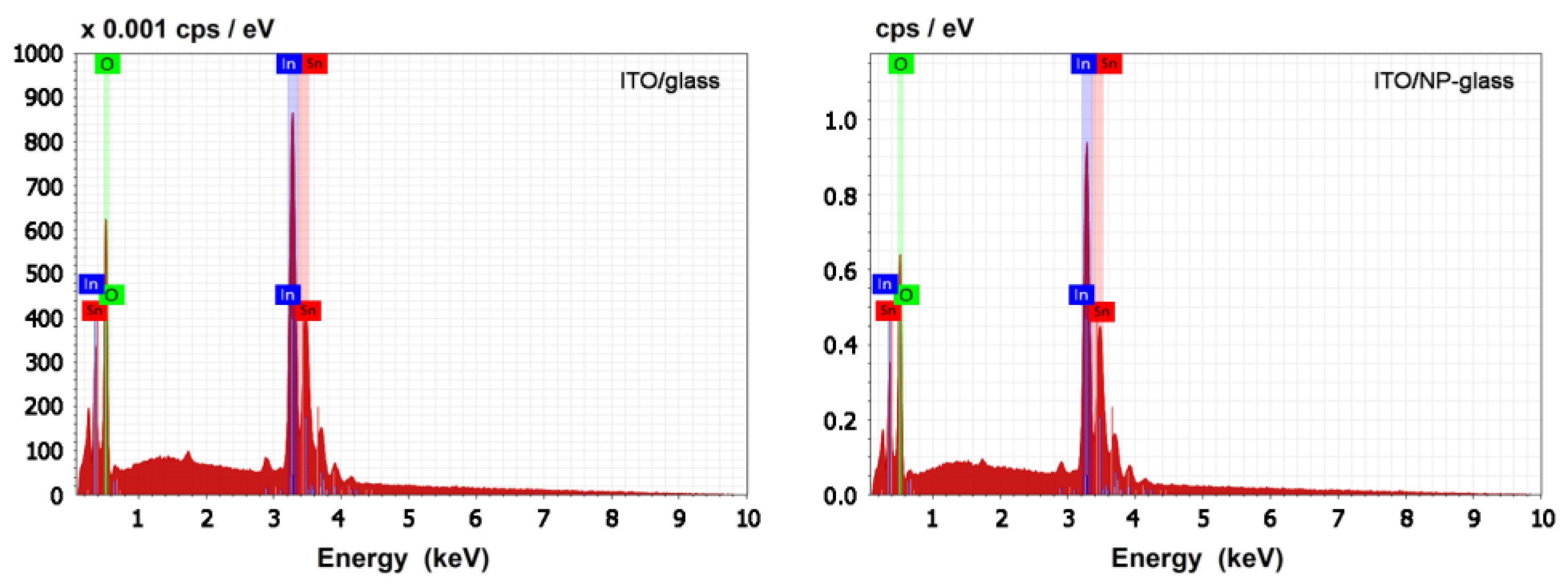
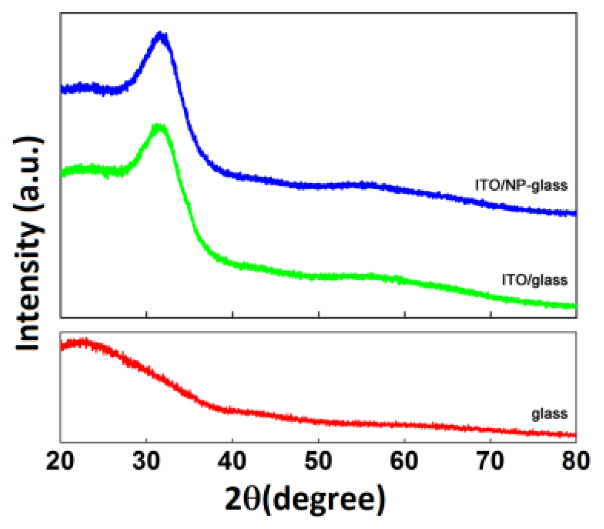
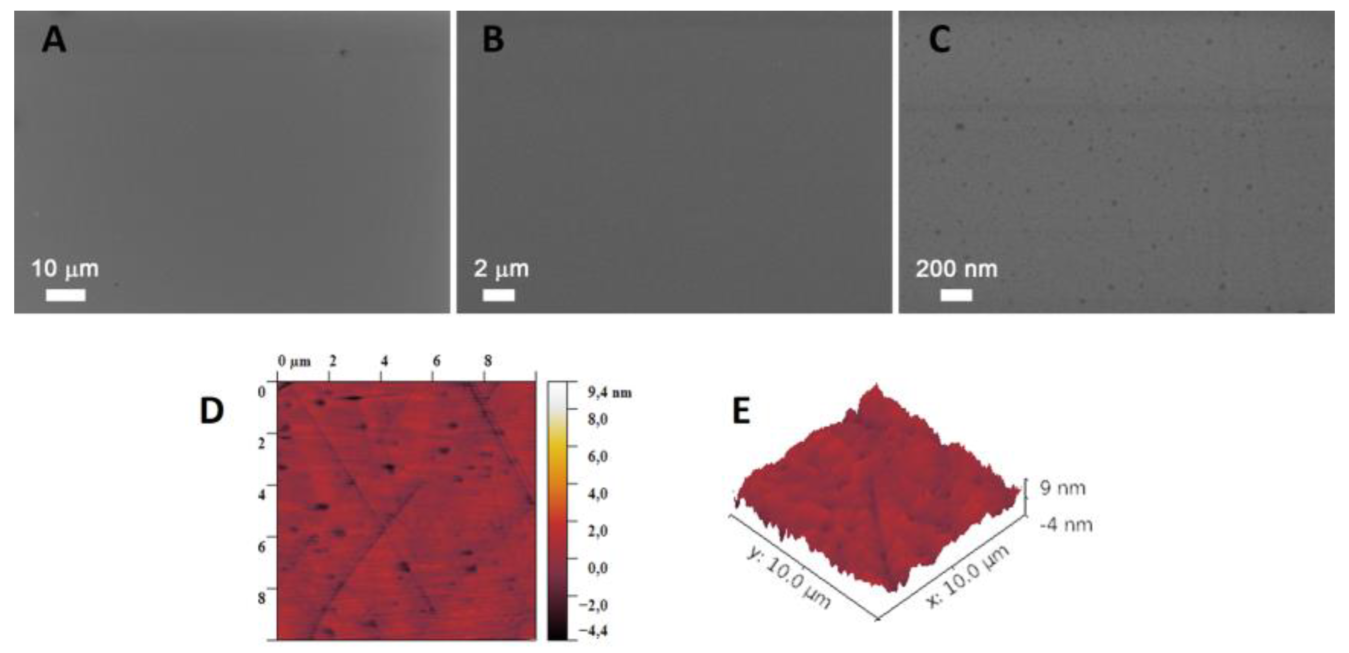
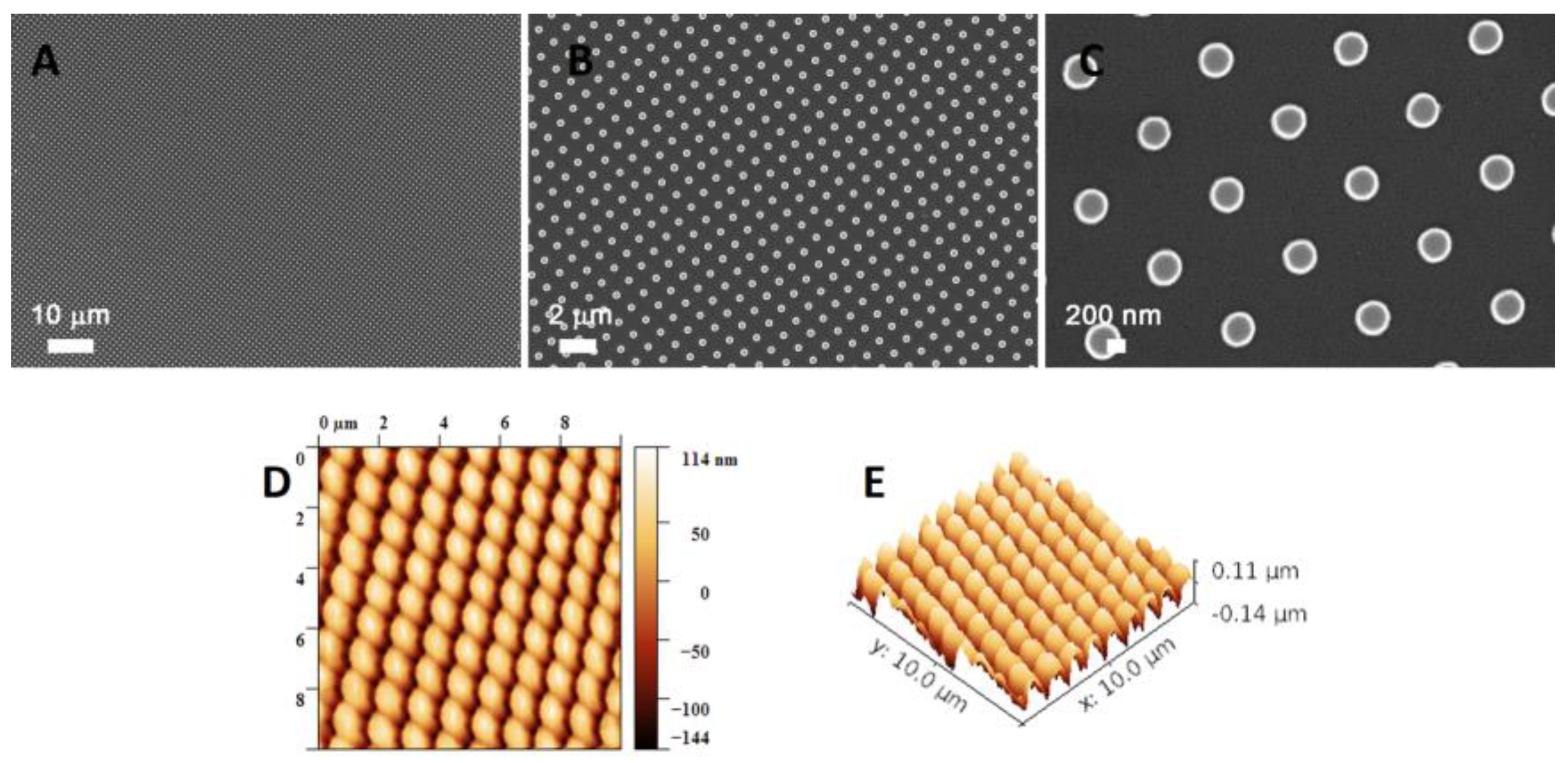
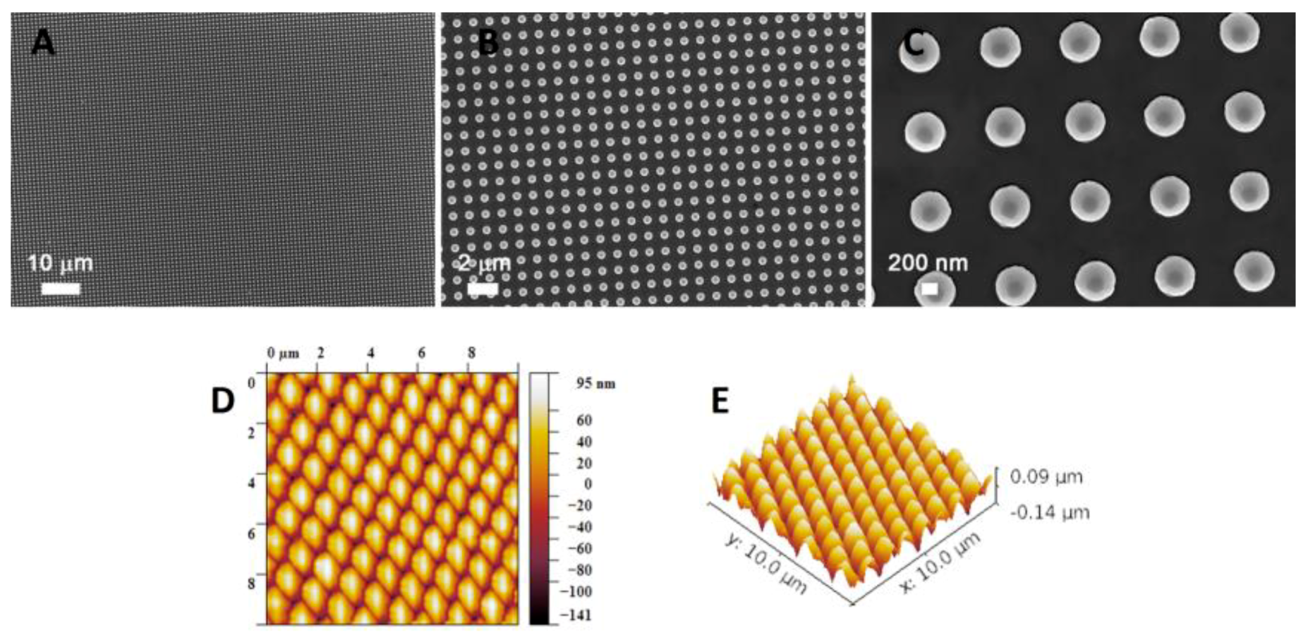
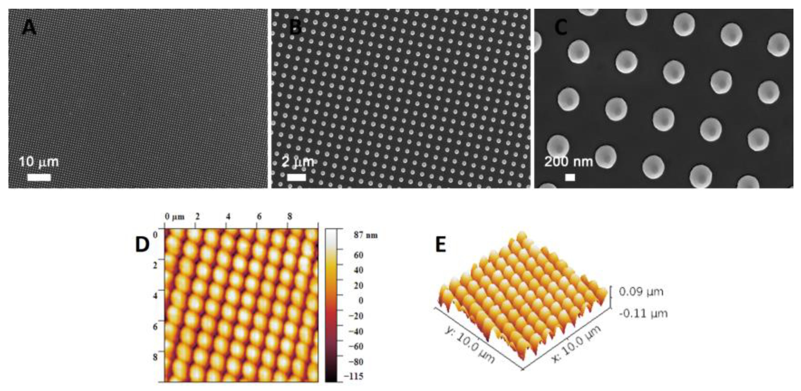
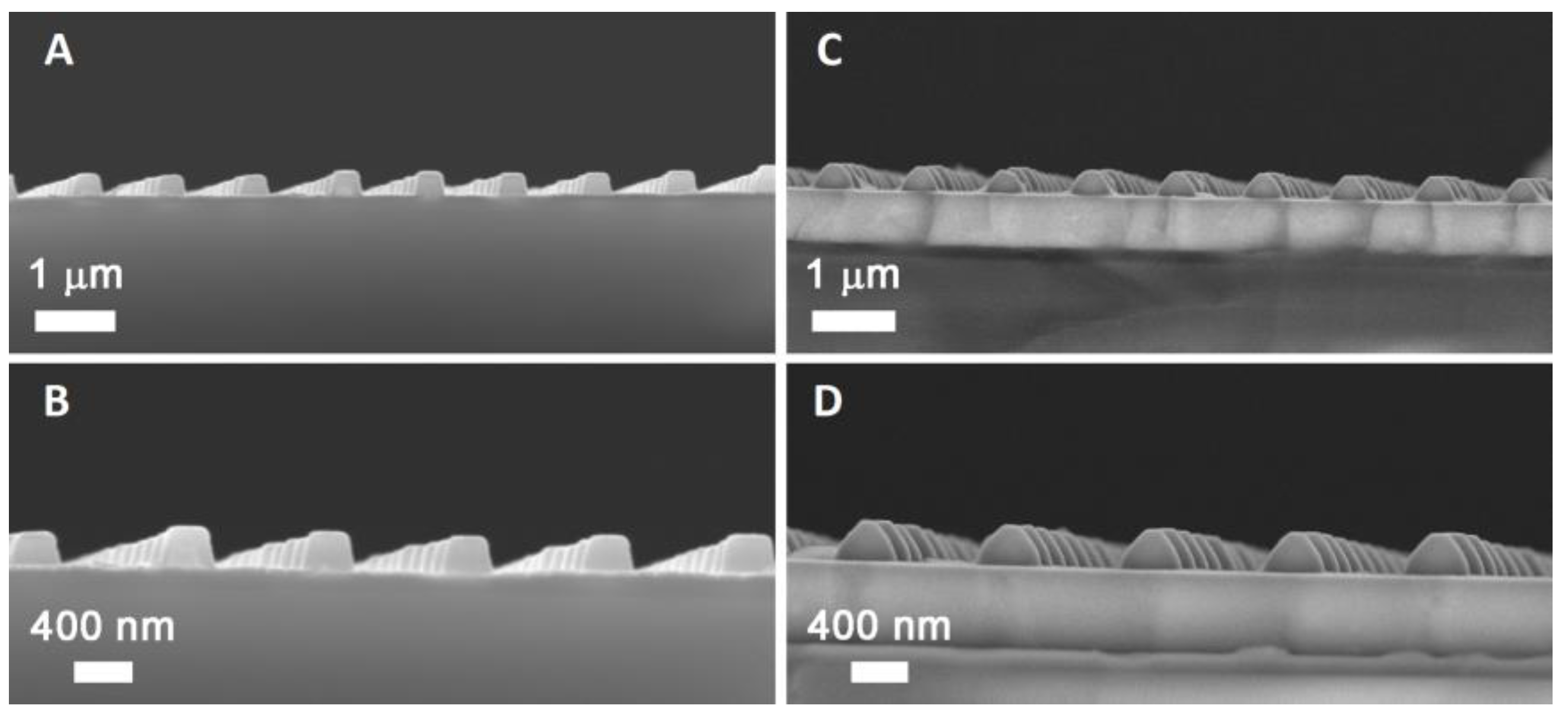
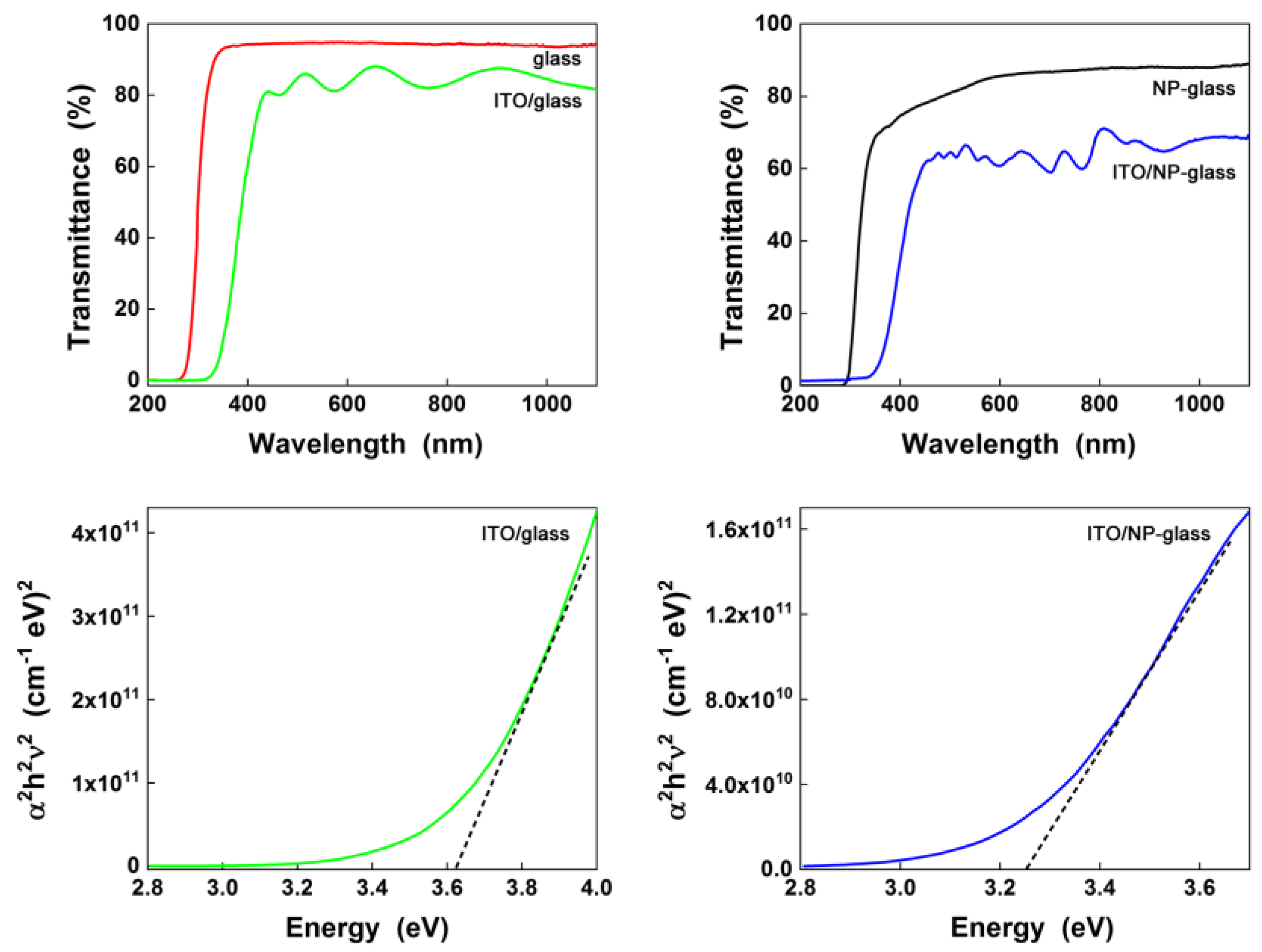
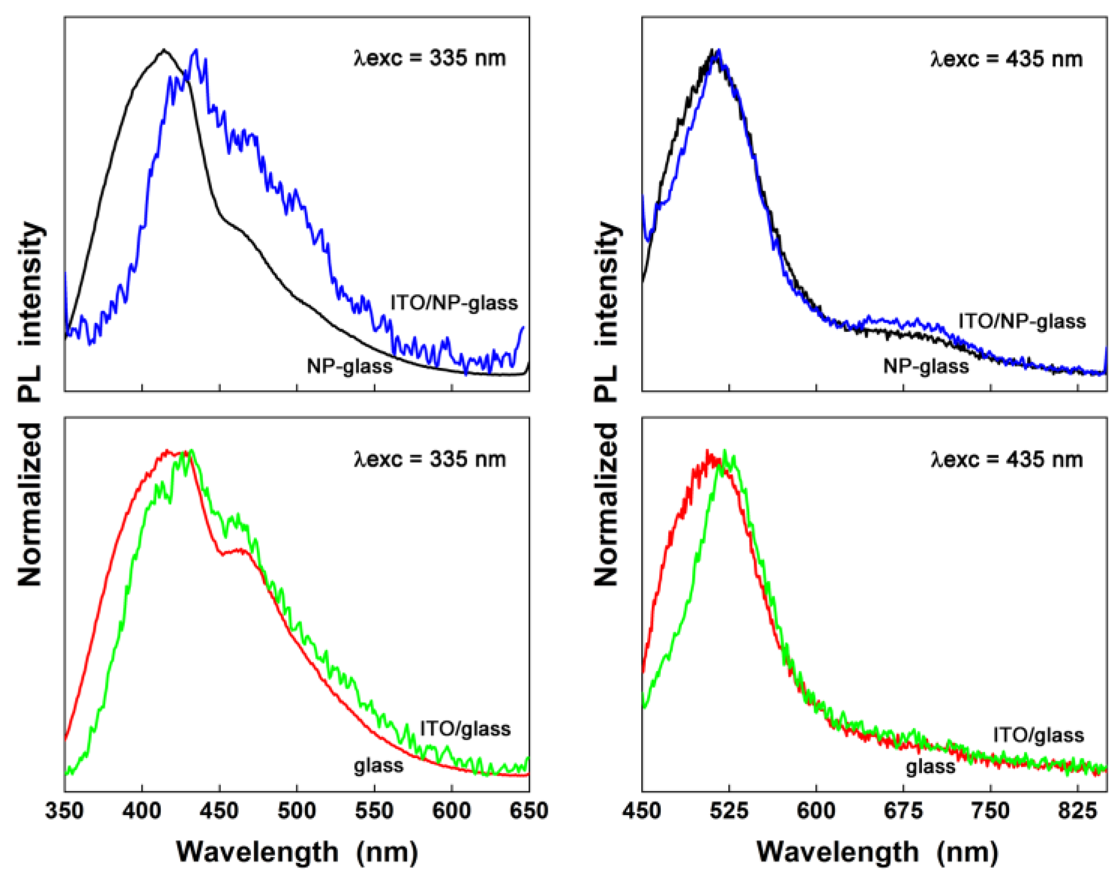
3. Results and Discussions

The elemental composition of the TCO films grown by PLD was evaluated by energy dispersive X-ray analysis (EDX), which is presented in the Figure 1. The EDX spectra of ITO/glass and ITO/NP-glass samples evidenced the presence of In, Sn, and O components. In both cases, the atomic percentage for Sn:O:In was found to be about 3.7:63.5:32.7, confirming that the PLD target composition was maintained in the deposited ITO film. The results are in agreement to those reported for ITO films obtained by PLD [35], as the technique allows a stoichiometric transfer of the material from the target to the deposited film. The other peaks observed in the EDX spectra originated from the glass used as deposition substrate.
As mentioned above, substrate temperature and oxygen pressure have determinant impact on the crystalline structure of the TCO films grown by PLD. Thus, the ITO/glass and ITO/NP-glass samples were investigated by X-ray diffraction (XRD). In Figure 2, the XRD patterns of the ITO films deposited on unheated substrates exhibit only a broad peak at ~31° which can be related to a microcrystalline structure with a preferred (222) orientation [36]. The result is consistent with other studies carried out on ITO films prepared by PLD at RT and low PO2, though with higher laser fluency (4 J/cm2) [37]. It was noticed that the patterning process has no influence on the ITO crystallinity.
Also, the morphology and the roughness of the TCO thin films are key features which influence their optical and electrical properties. Ergo, in the next step, all prepared samples were analyzed by field emission scanning electron microscopy (FESEM) and atomic force microscopy (AFM). These types of analyses for ITO/glass, NP-glass, ITO/NP-glass, and ITO/NP-glass_bis can be seen in Figure 3, Figure 4, Figure 5 and Figure 6, respectively.
The FESEM images of the ITO films deposited on flat glass substrate (Figure 3) disclose a smooth surface in accordance with observations reported in the case of ITO films prepared by solution-based fabrication methods [38].
In the case of the structures fabricated by UV–NIL on glass substrates, the FESEM images (Figure 4) show arrays of periodic pillars with diameters of ~350 nm and a distance between the pillars of ~1100 nm. As can be seen in Figure 5 and Figure 6, the deposition of the ITO by PLD resulted in the increase of the pillars’ width and the decrease of the separation step—the deposited films were trying to fill the space between pillars and to cover them.
Using the AFM investigations, the root mean square (RMS) parameter was evaluated as being: 1 nm for ITO/glass (Figure 3), 59 nm for NS-glass (Figure 4), 47 nm for ITO/NP-glass (Figure 5), and 44 nm for ITO/NP-glass_bis (Figure 6). The presence of the pillars lead, as was expected, to a roughness increase. In the case of the ITO/glass sample, the RMS value is lower in comparison with other values calculated for ITO films prepared by other methods [8], but it is comparable with those reported for ITO films grown by PLD, as this technique offers the possibility to obtain TCO films with a smooth surface when the deposition is made at low temperature and with a low laser fluency [19,39].
Additionally, the surface kurtosis (Rku) parameter, a peakedness indicator—also determined by AFM—has the following values: 5.2 for ITO/glass, 2.1 for NP-glass, 2.3 for ITO/NP-glass, and 2.4 for ITO/NP-glass_bis. Based on the Rku values, it can be mentioned that the ITO/glass film presents more peaks than valleys, while the ITO/NP-glass films present more valleys than peaks.
The EDX mapping images of the ITO films deposited on both flat (Figure 7A,B) and nanopatterned glass (Figure 7C,D) substrate illustrate a uniform distribution of the chemical elements Sn, O, and In contained in the PLD target. Over the fabricated pillars, no preferential arrangement of the elements as clusters is evidenced.
The height of the pillars obtained by UV-NIL was estimated at ~250 nm from the cross-sectional FESEM images shown in Figure 8A,B, as the height was reduced after their coating with ITO films Figure 8C,D. Furthermore, these FESEM images emphasize an interesting aspect: the shape of the pillars is changed after the deposition of the TCO towards a pyramid trunk-like shape.
The optical properties are presented in Figure 9 and Figure 10. The ITO film deposited on flat glass substrate presents a transmittance over 80% between 600 and 1100 nm, with the interference maxima and minima exhibited in the visible range being typical for the films with similar thickness (~340 nm) deposited by PLD or by magnetron sputtering [8,19]. The interference characteristics are also observed in the UV-VIS spectra of the ITO film deposited on nanopatterned glass substrate. Using these maxima and minima and the Swaneopel method [40], the refractive index (n) value was evaluated at ~1.9 for ITO/glass—a characteristic value for the ITO films deposited by PLD—and at ~2.4 for ITO/NP-glass. Some studies reported that the n value depended on the substrate temperature, since higher values were obtained for the ITO films prepared at a low temperature [19]. In addition, by plotting (αhν)2 versus photon energy, the band gap values for both ITO/glass and ITO/NP-glass samples were estimated at ~3.65 eV and ~3.21 eV, respectively. The band gap of ITO deposited on flat glass substrate is thickness-dependent and is in accordance with other reported films prepared by PLD with different SnO2 content (5% or 10%) [37,39]. It is well known that ITO is a semiconductor with a direct wide band gap greater than 3 eV [3]. The increase of this value is usually attributed to the increasing of the carrier density, a process known as Burstein-Moss effect [19]. Regarding the lowering of the band gap value of ITO film deposited on the nanopatterned glass substrate, a similar effect, related to oxygen deficiency, was observed for the ITO deposited by spin-coating on self-assembled polymer nanopattern [41].
The PL spectra of all investigated samples—recorded at two excitation wavelength (335 and 435 nm)—are shown in Figure 10, as such information is useful for the TCO applications in OPV or OLED devices [42]. Under UV excitation (335 nm), the ITO/glass sample revealed a structured emission band with peaks at about 410, 430, and 460 nm which can be attributed to the ITO [25,43]. Generally, these emissions are characteristic of ITO, appearing due to the In2O3 oxygen deficiencies [44]. However, it is difficult to make an assignment, since the glass substrate presents also a similar emission. The ITO/NP-glass sample disclosed a shift of the structured emission band compared with that of the NP/glass sample. Furthermore, the shoulder at about 500 nm can also be associated with the ITO emission [45]. Under visible excitation (435 nm), an emission band peaked at about 550 nm is evidenced by the ITO/glass sample being narrower in comparison with that of the glass substrate [46]. In the case of the patterned samples, the PL spectra near the emission band at 550 nm show another weak broad emission band between 600 and 800 nm, which can be as also related the deposited ITO film [46].
The electrical properties of the ITO films deposited on flat and nanopatterned glass substrate by PLD were evaluated from the Hall measurements (Table 1), which revealed that the electrons are the charge carriers.
The calculated electrical resistivity is lower for the ITO/glass sample in comparison with the values for ITO/NP/glass and ITO/NP-glass_bis samples. Therefore, ITO samples prepared by PLD on substrates maintained at RT have resistivity values close to those reported for the ITO films deposited by PLD using a heated substrate (300 °C)—a target with 5% SnO2, with the TCO film having 30 nm in thickness [17]. Our ITO samples are also similar to ITO films deposited using a 1 Pa O2 atmosphere, a target having 10% SnO2 content and different temperature substrate (beginning from 100 °C) [39,47]. In addition, the resistivity of the ITO/glass sample has a better value (1.8 × 10⁻⁴ Ω·cm) relative to others obtained in similar PLD experimental parameters (substrate kept at RT, SnO2 content, oxygen pressure) [48]. As mentioned above, the oxygen pressure is a key parameter in the PLD, as it influences the resistivity value of the TCO films—an influence owing to the number of formed oxygen vacancies in the laser transferred ITO films [25]. Thus, the electrical resistivity decreases with the increase of the SnO2 content over 5%. The increasing of the Sn amount leads to a higher concentration of the electron traps [19]. In our case, the ITO/glass sample has the highest carrier concentration (3.3 × 1021 cm−3), the values of the ITO/NP-glass and ITO/NP-glass_bis samples being similar. The results are in consensus with other results obtained for ITO samples prepared on heated substrate [19,48]. Also, in these studies, the carrier density is related to the Sn quantity, an increase in the carrier density being reported as effect of the Sn donor electrons for the samples grown from the target containing a higher Sn concentration [19]. The carrier density is connected to the band gap value: ITO/glass samples that featured the highest carrier density had Eg = 3.65 eV, whereas ITO/NP-glass characterized by a lower carrier density has Eg = 3.21 eV. Furthermore, an increase in the Hall mobility was evidenced for the ITO/NP-glass and ITO/NP-glass_bis samples—15.1 and 14.6 cm2/Vs, respectively—compared to the ITO/glass sample—10.6 cm2/Vs—which has smaller values than other reported values [25] due to the carrier-carrier scattering as an effect of high carrier density [1]. Taking into consideration that the only difference between the samples investigated in this study was the use of different substrate type, the increase in the Hall mobility for the ITO films deposited by PLD on nanopatterned glass is clearly owed to this patterned substrate.

4. Conclusions

PLD is an adequate technique to deposit ITO films on both flat and patterned glass substrates at room temperature, 1.2 J/cm2 laser fluency, and low oxygen pressure (1.5 Pa). The patterned substrates containing periodic pillars with ~350 nm in width, ~250 nm in height, and ~1100 nm separation step were fabricated by a UV-NIL process. The EDX analysis confirms that the laser-deposited ITO films preserve the stoichiometry of the solid ITO target (In2O3:SnO2 = 90%:10% weight), and the XRD data show a (222) preferential orientation for the grown film. The SEM and AFM images prove that the deposited ITO films retain the pattern of the glass substrates, while the nanopatterned TCO films featured a good optical transmittance. A low RMS value (1 nm) was estimated for the ITO film deposited on flat glass. The optical band gap and the refractive index were evaluated from the UV-VIS spectra, and the obtained values were in agreement with other results reported for ITO films deposited by PLD. The electrical measurements revealed that a n-type semiconductor was obtained, as the TCO films were characterized by a low electrical resistivity (<2.8 × 10⁻⁴) regardless the substrate type. However, an increase in the Hall mobility was observed in the case of the ITO films deposited on nanostructured glass. By combining UV-NIL—a cost-effective technique to fabricate nanopatterns on large areas—and PLD, a method for growing TCO films at low substrate temperature can be obtained for nanopatterned ITO films. This could have applications in organic photovoltaic cells or organic light emitting devices.

Author Contributions

Conceptualization, M.S.; Methodology, M.S. and N.P.; Validation, M.S., N.P. and G.S.; Formal Analysis, A.C., F.G. and G.S.; Investigation, A.C., N.P., G.S., F.G., O.R. and C.B.; Resources, G.S. and A.S.; Writing—Original Draft Preparation, M.S.; Writing—Review and Editing, N.P. and F.G.; Supervision, G.S. and A.S.

Funding

This research was funded by the Romanian Ministry of Research and Innovation through National Core Program from PN18-110101 and LAPLAS V (3N/2018) contracts and from ROSA STAR 179/2017 contract.

Conflicts of Interest

The authors declare no conflict of interest.

References

  1. Eason, R. Pulsed Laser Deposition of Thin Films: Applications-Led Growth of Functional Materials; John Wiley & Sons, Inc.: Hoboken, NJ, USA, 2007; pp. 240–255. [Google Scholar]
  2. Bright, C.I. Review of transparent conductive oxides (TCO). In 50 Years of Vacuum Coating Technology and the Growth of the Society of Vacuum Coaters; Society of Vacuum Coaters: Materials Park, OH, USA, 2007. [Google Scholar]
  3. Afre, R.A.; Sharma, N.; Sharon, M.; Sharon, M. Transparent conducting oxide films for various applications: A review. Rev. Adv. Mater. Sci. 2018, 53, 79–89. [Google Scholar]
  4. Hosono, H.; Ueda, K. Transparent conductive oxides. In Springer Handbook of Electronic and Photonic Materials; Kasap, S., Capper, P., Eds.; Springer: Berlin, Germany, 2017; pp. 1391–1404. [Google Scholar]
  5. Cao, W.; Li, J.; Chen, H.; Xue, J. Transparent electrodes for organic optoelectronic devices: A review. J. Photonics Energy 2014, 4, 040990. [Google Scholar] [CrossRef]
  6. Hosono, H.; Kim, J.; Toda, Y.; Kamiya, T.; Watanabe, S. Transparent amorphous oxide semiconductors for organic electronics: Application to inverted OLEDs. Pro. Nati. Acad. Sci. 2017, 114, 233–238. [Google Scholar] [CrossRef] [PubMed]
  7. Mbule, P.; Wang, D.; Grieseler, R.; Schaaf, P.; Muhsin, B.; Hoppe, H.; Mothudi, B.; Dhlamini, M. Aluminum-doped ZnO thin films deposited on flat and nanostructured glass substrates: Quality and performance for applications in organic solar cells. Sol. Energy 2018, 172, 219–224. [Google Scholar] [CrossRef]
  8. Prepelita, P.; Filipescu, M.; Stavarache, I.; Garoi, F.; Craciun, D. Transparent thin films of indium tin oxide: Morphology–optical investigations, inter dependence analyzes. Appl. Surf. Sci. 2017, 424, 368–373. [Google Scholar] [CrossRef]
  9. Starkov, I.A.; Nyapshaev, I.A.; Starkov, A.S.; Abolmasov, S.N.; Abramov, A.S.; Levitskii, V.S.; Terukov, E.I. Influence of substrate movement on the ITO film thickness distribution during magnetron sputtering. J. Vac. Sci. Technol. A Vac. Surf. Films 2017, 35, 061301. [Google Scholar] [CrossRef]
  10. Meng, L.J.; Gao, J.; Silva, R.A.; Song, S. Effect of the oxygen flow on the properties of ITO thin films deposited by ion beam assisted deposition (IBAD). Thin Solid Films 2008, 516, 5454–5459. [Google Scholar] [CrossRef] [Green Version]
  11. Kim, S.J.; Choi, S.Y.; Choi, K. Preparation and characterization of ITO thin films deposition by ion beam assisted deposition. J. Korean Inst. Met. Mater. 2014, 52, 475–484. [Google Scholar] [CrossRef]
  12. Atabaev, I.G.; Hajiev, M.U.; Pak, V.A. Growth of ITO films by modified chemical vapor deposition method. Int. J. Thin Films Sci. Technol. 2016, 5, 13–16. [Google Scholar]
  13. Nishinaka, H.; Yoshimoto, M. Mist chemical vapor deposition of single-phase metastable rhombohedral indium tin oxide epitaxial thin films with high electrical conductivity and transparency on various α-Al2O3 substrates. Cryst. Growth Des. 2018, 18, 4022–4028. [Google Scholar] [CrossRef]
  14. Socol, G.; Socol, M.; Stefan, N.; Axente, E.; Popescu-Pelin, G.; Craciun, D.; Duta, L.; Mihailescu, C.N.; Mihailescu, I.N.; Stanculescu, A.; et al. Pulsed laser deposition of transparent conductive oxide thin films on flexible substrates. Appl. Surf. Sci. 2012, 260, 42–46. [Google Scholar] [CrossRef]
  15. Craciun, V.; Chiritescu, C.; Kelly, F.; Singh, R.K. Low temperature growth of smooth indium tin oxide films by ultraviolet assisted pulsed laser deposition. J. Optoelectron. Adv. Mater. 2002, 4, 21–25. [Google Scholar]
  16. Ohta, H.; Orita, M.; Hirano, M.; Tanji, H.; Kawazoe, H.; Hosono, H. Highly electrically conductive indium-tin-oxide thin films epitaxially grown on yttria-stabilized zirconia (100) by pulsed-laser deposition. Appl. Phys. Lett. 2000, 76, 2740–2742. [Google Scholar] [CrossRef]
  17. Suzuki, A.; Mastsushita, T.; Aoki, T.; Yoneyama, Y.; Okuda, M. Pulsed laser deposition of transparent conducting indium tin oxide films in magnetic field perpendicular to plume. Jpn. J. Appl. Phys. 2001, 40, L401. [Google Scholar] [CrossRef]
  18. Kim, H.; Horwitz, J.S.; Pique, A.; Gilmore, C.M.; Chrisey, D.B. Electrical and optical properties of indium tin oxide thin films grown by pulsed laser deposition. Appl. Phys. A 1999, 69, S447–S450. [Google Scholar] [CrossRef]
  19. Kim, H.; Gilmore, C.M.; Pique´, A.; Horwitz, J.S.; Mattoussi, H.; Murata, H.; Kafafi, Z.H.; Chrisey, D.B. Electrical, optical, and structural properties of indium-tin-oxide thin films for organic light-emitting devices. J. Appl. Phys. 1999, 86, 6451–6461. [Google Scholar] [CrossRef]
  20. Bi, Y.-G.; Feng, J.; Ji, J.-H.; Yi, F.-S.; Li, Y.-F.; Liu, Y.-F.; Zhang, X.-L.; Sun, H.-B. Nanostructures induced light harvesting enhancement in organic photovoltaics. Nanophotonics 2018, 7, 371–391. [Google Scholar] [CrossRef]
  21. Ferry, V.E.; Verschuuren, M.A.; Lare, M.C.V.; Schropp, R.E.; Atwater, H.A.; Polman, A. Optimized spatial correlations for broadband light trapping nanopatterns in high efficiency ultrathin film a-Si:H solar cells. Nano Lett. 2011, 11, 4239–4245. [Google Scholar] [CrossRef]
  22. Choo, S.; Choi, J.; Choi, H.-J.; Huh, D.; Son, S.; Kim, Y.D.; Lee, H. Enhancement of light extraction efficiency for GaN-based light emitting diodes using ZrO2 high-aspect-ratio pattern as scattering layer. Ceram. Int. 2017, 43, S609–S612. [Google Scholar] [CrossRef]
  23. Saxena, K.; Jain, V.K.; Mehta, D.S. A review on the light extraction techniques in organic electroluminescent devices. Opt. Mater. 2009, 32, 221–233. [Google Scholar] [CrossRef]
  24. Tseng, A.A.; Chen, K.; Chen, C.D.; Ma, K.J. Electron beam lithography in nanoscale fabrication: Recent development. IEEE Trans. Electron. Packag. Manuf. 2003, 26, 141–149. [Google Scholar] [CrossRef]
  25. Breazu, C.; Preda, N.; Socol, M.; Stanculescu, F.; Matei, E.; Stavarache, I.; Iordache, G.; Girtan, M.; Rasoga, O.; Stanculescu, A.I. Investigations on the properties of a two-dimensional nanopatterned metallic electrode. Dig. J. Nanomater. Biostructures 2016, 11, 1213–1229. [Google Scholar]
  26. Matsui, S. Three-dimensional nanostructure fabrication by focused-ion-beam chemical-vapor-deposition. Microsc. Microanal. 2006, 12, 130–131. [Google Scholar] [CrossRef]
  27. Guo, L.J. Recent progress in nanoimprint technology and its applications. J. Phys. D Appl. Phys. 2004, 37, R123. [Google Scholar] [CrossRef]
  28. Lee, H.; Hong, S.; Yang, K.; Choi, K. Fabrication of nano-sized resist patterns on flexible plastic film using thermal curing nano-imprint lithography. Microelectron. Eng. 2006, 83, 323–327. [Google Scholar] [CrossRef]
  29. Austin, M.D.; Ge, H.; Wu, W.; Li, M.; Yu, Z.; Wasserman, D.; Lyon, S.A.; Chou, S.Y. Fabrication of 5 nm linewidth and 14 nm pitch features by nanoimprint lithography. Appl. Phys. Lett. 2004, 84, 5299–5301. [Google Scholar] [CrossRef]
  30. Akita, Y.; Sugimoto, Y.; Kobayashi, K.; Suzuki, T.; Oi, H.; Mita, M.; Yoshimoto, M. Crystal growth control of functional oxide thin films on nanopatterned substrate surfaces. J. Laser Micro/Nanoeng. 2009, 4, 202–206. [Google Scholar] [CrossRef]
  31. Akita, Y.; Miyake, Y.; Nakai, H.; Oi, H.; Mita, M.; Kaneko, S.; Mitsuhashi, M.; Yoshimoto, M. Evolution of atomically stepped surface of indium tin oxide thin films grown on nanoimprinted glass substrates. Appl. Phys. Express 2011, 4, 035201. [Google Scholar] [CrossRef]
  32. Liu, Y.; Kirsch, C.; Gadisa, A.; Aryal, M.; Mitran, S.; Samulski, E.T.; Lopez, R. Effects of nano-patterned versus simple flat active layers in upright organic photovoltaic devices. J. Phys. D Appl. Phys. 2013, 46, 024008. [Google Scholar] [CrossRef]
  33. Stanculescu, A.; Socol, M.; Socol, G.; Mihailescu, I.N.; Girtan, M.; Preda, N.; Albu, A.-M.; Stanculescu, F. Effect of maleic anhydride-aniline derivative buffer layer on the properties of flexible substrate heterostructures: Indium tin oxide/nucleic acid base/metal. Thin Solid Films 2011, 520, 1251–1258. [Google Scholar] [CrossRef]
  34. Stanculescu, A.; Rasoga, O.; Preda, N.; Socol, M.; Stanculescu, F.; Ionita, I.; Albu, A.-M.; Socol, G. Preparation and characterization of polar aniline functionalized copolymers thin films for optical non-linear applications. Ferroelectrics 2009, 389, 159–173. [Google Scholar] [CrossRef]
  35. Tseng, K.-S.; Lo, Y.-L. Effects of cumulative ion bombardment on ITO films deposited on PET and Si substrates by DC magnetron sputtering. Opt. Mater. Express 2014, 4, 764–775. [Google Scholar] [CrossRef]
  36. Ohshima, T.; Matsunaga, T.; Kawasaki, H.; Suda, Y.; Yagyu, Y. Preparation of ITO thin films by pulsed laser deposition for use as transparent electrodes in electrochromic display devices. Trans. Mater. Res. Soc. Jpn. 2010, 35, 583–587. [Google Scholar] [CrossRef]
  37. Schou, J. Physical aspects of the pulsed laser deposition technique: The stoichiometric transfer of material from target to film. Appl. Surf. Sci. 2009, 255, 5191–5198. [Google Scholar] [CrossRef]
  38. Chen, Z.; Li, W.; Li, R.; Zhang, Y.; Xu, G.; Cheng, H. Fabrication of highly transparent and conductive indium-tin oxide thin films with a high figure of merit via solution processing. Langmuir 2013, 29, 13836–13842. [Google Scholar] [CrossRef] [PubMed]
  39. Kim, S.H.; Park, N.M.; Kim, T.; Sung, G.Y. Electrical and optical characteristics of ITO films by pulsed laser deposition using a 10 wt.% SnO2-doped In2O3 ceramic target. Thin Solid Films 2005, 475, 262–266. [Google Scholar] [CrossRef]
  40. Swanepoel, R. Determination of surface roughness and optical constants of inhomogeneous amorphous silicon films. J. Phys. E Sci. Instrum. 1984, 17, 896–903. [Google Scholar] [CrossRef]
  41. Xia, G.; Wang, S. Solution patterning of ultrafine ITO and ZnRh2O4 nanowire array below 20 nm without etching process. Nanoscale 2011, 3, 3598–3600. [Google Scholar] [CrossRef]
  42. Babu, S.H.; Rao, N.M.; Kaleemulla, S.; Amarendra, G.; Krishnamoorthi, C. Room-temperature ferromagnetic and photoluminescence properties of indium–tin-oxide nanoparticles synthesized by solid-state reaction. Bull. Mater. Sci. 2017, 40, 17–23. [Google Scholar] [CrossRef]
  43. Luo, S.; Kohiki, S.; Okada, K.; Shoji, F.; Shishido, T. Hydrogen effects on crystallinity, photoluminescence, and magnetization of indium tin oxide thin films sputter-deposited on glass substrate without heat treatment. Phys. Status Solidi A 2010, 207, 386–390. [Google Scholar] [CrossRef]
  44. Lee, M.S.; Choi, W.C.; Kim, E.K.; Kim, C.K.; Min, S.K. Characterization of the oxidized indium thin films with thermal oxidation. Thin Solid Films 1996, 279, 1–3. [Google Scholar] [CrossRef]
  45. Thirumoorthi, M.; Thomas Joseph Prakash, J. Structure, optical and electrical properties of indium tin oxide ultrathin films prepared by jet nebulizer spray pyrolysis technique. J. Asian Ceram. Soc. 2016, 4, 124–132. [Google Scholar] [CrossRef]
  46. Venkatesh, P.S.; Ramakrishnan, V.; Jeganathan, K. Vertically aligned indium doped zinc oxide nanorods for the application of nanostructured anodes by radio frequency magnetron sputtering. CrystEngComm 2012, 14, 3907–3914. [Google Scholar] [CrossRef]
  47. Fang, X.; Mak, C.L.; Zhang, S.; Wang, Z.; Yuan, W.; Ye, H. Pulsed laser deposited indium tin oxides as alternatives to noble metals in the near-infrared region. J. Phys. Condens. Matter 2016, 28, 224009. [Google Scholar] [CrossRef] [PubMed] [Green Version]
  48. Wu, Y.; Maree, C.H.M.; Haglund, R.F., Jr.; Hamilton, J.D.; Morales Paliza, M.A.; Huang, M.B.; Feldman, L.C.; Weller, R.A. Resistivity and oxygen content of indium tin oxide films deposited at room temperature by pulsed-laser ablation. J. Appl. Phys. 1999, 86, 991–994. [Google Scholar] [CrossRef]
Figure 1. Energy dispersive X-ray analysis (EDX) spectra of indium tin oxide ITO/glass and ITO/nanopatterned (NP)-glass samples.
Coatings 09 00019 g001
Figure 2. X-ray diffraction (XRD) patterns of glass, ITO/glass and ITO/NP-glass samples.
Coatings 09 00019 g002
Figure 3. Field emission scanning electron microscopy (FESEM) images at different magnifications (A,B,C) and atomic force microscopy (AFM) images (D,E) in 2D and 3D format of the ITO/glass sample.
Coatings 09 00019 g003
Figure 4. FESEM images at different magnifications (A,B,C) and AFM images (D,E) in 2D and 3D format of the NP-glass sample.
Coatings 09 00019 g004
Figure 5. FESEM images at different magnifications (A,B,C) and AFM images (D,E) in 2D and 3D format of the ITO/NP-glass sample.
Coatings 09 00019 g005
Figure 6. FESEM images at different magnifications (A,B,C) and AFM images (D,E) in 2D and 3D format of the ITO/NP-glass_bis sample.
Coatings 09 00019 g006
Figure 7. FESEM (A,C) and EDX mapping (B,D) images of ITO/glass (A,B) and ITO/NP-glass (C,D) samples.
Coatings 09 00019 g007
Figure 8. Cross-sectional FESEM images at two magnifications of NP-glass (A,B) and ITO/NP-glass (C,D) samples.
Coatings 09 00019 g008
Figure 9. UV-VIS spectra and (αhν)2 vs. E dependency of ITO/glass and ITO/NP-glass samples.
Coatings 09 00019 g009
Figure 10. Photoluminescence (PL) spectra at two excitation wavelengths of glass, NP-glass, ITO/glass and ITO/NP-glass samples.
Coatings 09 00019 g010
Table 1. Electrical parameters of the ITO deposited by PLD estimated from the Hall measurements.
SampleResistivity (Ωcm)Mobility (cm2/Vs)Carrier Concentration (cm−3)Sheet Resistance (Ω/sq)
ITO/glass1.8 × 10−410.63.3 × 10215.3
ITO/NP-glass2.8 × 10−415.11.5 × 10218
ITO/NP-glass_bis2.7 × 10−414.61.6 × 10217.9

