Article

The Effect of Energy Level of Transport Layer on the Performance of Ambient Air Prepared Perovskite Solar Cell: A SCAPS-1D Simulation Study

1
School of Physics, East China University of Science and Technology, 130 Meilong Road, Shanghai 200237, China
2
Department of Applied Physics, Graduate School of Engineering, Osaka University, Yamadaoka, Suita-City 565-0871, Osaka, Japan
*
Author to whom correspondence should be addressed.
Crystals 2022, 12(1), 68; https://doi.org/10.3390/cryst12010068
Submission received: 7 December 2021 / Revised: 22 December 2021 / Accepted: 27 December 2021 / Published: 4 January 2022

Abstract

:
The perovskite solar cell (PSC) as an emerging and promising type has been extensively studied. In this study, a model for a PSC prepared in ambient air was established by using SCAPS-1D. After that, it was further analyzed through varying the defect density of the perovskite absorber layer (Nt), the thin film thickness and energy-level matching between the electron transport layer (ETL), the perovskite absorber layer and the hole transport layer (HTL), for a better understanding of the carrier features. The Nt varied from 1.000 × 10¹¹ to 1.000 × 1017 cm−3. The performance of the solar cell is promoted with improved Nt. When Nt is at 1.000 × 1015 cm−3, the carrier diffusion length reaches μm, and the carrier lifetime comes to 200 nm. The thickness of the absorber layer was changed from 200 to 600 nm. It is shown that the absorber layer could be prepared thinner for reducing carrier recombination when at high Nt. The thickness effect of ETL and HTL is weakened, since Nt dominates the solar cell performance. The effect of the affinity of ETL (3.4–4.3 eV) and HTL (2.0–2.7 eV), together with three energy-level matching situations “ETL(4.2)+HTL(2.5)”, “ETL(4.0)+HTL(2.2)” and “ETL(4.0)+HTL(2.5)” on the performance of the solar cell were analyzed. It was found that the HTL with valence band 0.05 eV lower than that of the perovskite absorber layer could have a blocking effect that reduced carrier recombination. The effect of energy-level matching becomes more important with improved Nt. Energy-level matching between the ETL and perovskite absorber layer turns out counterbalance characteristic on Jsc and Voc, and the “ETL(4.0)+HTL(2.5)” case can result in solar cell with Jsc of 27.58 mA/cm2, Voc of 1.0713 V, FF of 66.02% and efficiency of 19.51%. The findings would be very useful for fabricating high-efficiency and low-cost PSC by a large-scale ambient air route.

1. Introduction

Perovskite, due to its outstanding optoelectronic and material properties (for example, high optical absorption coefficient, large carrier lifetime, balanced electron–hole diffusion length and efficient ambipolar charge transport [1,2,3]) together with a defect-tolerant nature and easy fabrication from solution [4,5,6,7,8,9], has provided enormous potential to trigger a revolution in solar-to-electricity conversion for the coming generation. Perovskite generally has the formula of ABX3, where A is CH3NH3+, CH(NH2)2+ or Cs+, B is Pb2+ or Sn2+ and X is I, Br or Cl [10]. Additionally, it has obtained tremendous attention since perovskite was introduced into a dye-sensitized solar cell as a solid-state light absorber layer in 2009 [1]. The power conversion efficiency of the perovskite solar cell (PSC) has been boosted rapidly and it has now reached a certified 25.2% [11], which is comparable to or even exceeds other well-studied solar cells such as CuInxGa1−x(S,Se)2, CdTe or polycrystalline silicon solar cells [12,13,14,15].
PSCs generally consist of a 200–600 nm photoactive absorber layer, sandwiched between two charged transport layers (TL), the electron transport layer (ETL) and the hole transport layer (HTL) that have the function of selectively transporting the photo-generated electrons and holes to the cathode and anode, respectively. The solar cell that effectively converts solar radiation into electrical power needs to absorb the incident photons by the absorber layer and create charge carriers inside the absorber layer, and then separate the carriers at the absorber layer/TL interfaces and transport them through the TL to the external circuit. In an ideal solar cell, all incident photons are absorbed by the absorber layer, generating electrons and holes with unit efficiency. In the open-circuit condition, the only recombination channel is the radiative recombination of free electrons and holes. In principle, this would allow open-circuit voltages (Voc) close to the radiative limit. However, the commonly reported values for Voc are much lower due to unwanted nonradiative recombination [16]. This is the main reason that the experimental efficiency is still far from the Shockley–Queisser theoretical efficiency of up to 30% [17], despite the tremendous effort that has been devoted by the scientific community on the improvement of PSC technology. In past years, many studies have been conducted for identifying the possible nonradiative recombination channel [18,19,20,21]. More recently, measurements of the photoluminescence quantum yield on individual perovskite/TL junctions have been used to interpret the lossy Voc through quasi-Fermi level splitting (QFLS) losses in perovskite bulk [22,23,24,25]. The selectivity of a TL is defined as its ability to maintain the QFLS of the absorber layer while providing efficient majority carrier extraction. Despite these advances, however, the relation between the internal QFLS and the external Voc remains poorly understood today. The significance and impact of energy-level alignment remains as important now, and it even has become a heavily debated topic in the PSC field. For example, several studies have shown that the energy-level alignment between the perovskite and the TL is beneficial, while other studies do not agree with this view [26,27,28,29,30]. Therefore, to exploit the full potential of the magical perovskite material for solar cells, a more comprehensive understanding of the underlying physical processes and loss characteristics is still essential. In particular, the dynamic influence characteristics of the energy-level alignment with varied Nt has not been reported yet.
On the other hand, almost all of state-of-the-art PSCs nowadays are fabricated inside a glove-box with controlled atmospheric conditions. For example, most highly efficient PSCs are prepared inside a nitrogen- or argon-filled glove-box (H2O < 0.1 ppm and O2 < 0.1 ppm). This significantly limits the scaling-up of fabrication processes and also causes an extra budget for atmosphere control during the fabrication [31,32]. In recent years, PSCs are hungry for air atmosphere preparation technology in order to realize commercial production as soon as possible. Therefore, several studies have been conducted on the preparation of perovskite absorber layer under open ambient air. Several fabrication methods such as anti-solvent [33], dual-step thermal engineering technique [34] and crystal engineering [35] have been reported. The property of the PSC prepared under ambient air is acceptable as compared to that prepared in inert conditions [34,35,36,37], which offers a very promising way to large-scale industrial production of PSC. In such ambient air, the prepared PSC may produce different or important underlying physical processes and loss characteristics, which would call for more studies.
For these purposes, in this work, the characteristics of ambient air prepared PSC were studied by employing the SCAPS-1D software (ver.3.3.07, developed by Prof. Burgelman and his team at the University of Ghent, Belgium). First, a model was built with experimental parameters from the virtual ambient air fabricated PSC and other well-known published parameters [38,39,40,41]. The simulation results coming from the SCAPS-1D fitted well with the experimental results, indicating the built model is feasible. Then, the defect density of the perovskite absorber layer (Nt) and the thin film thickness were analyzed by using the SCAPS-1D. Finally, the dynamic influence characteristics of the energy-level alignment with varied Nt on the carrier generation, recombination and transport were investigated in detail by the SCAPS-1D, for understanding of the underlying physical processes and loss characteristics in the ambient air processed PSC.

2. Methodology

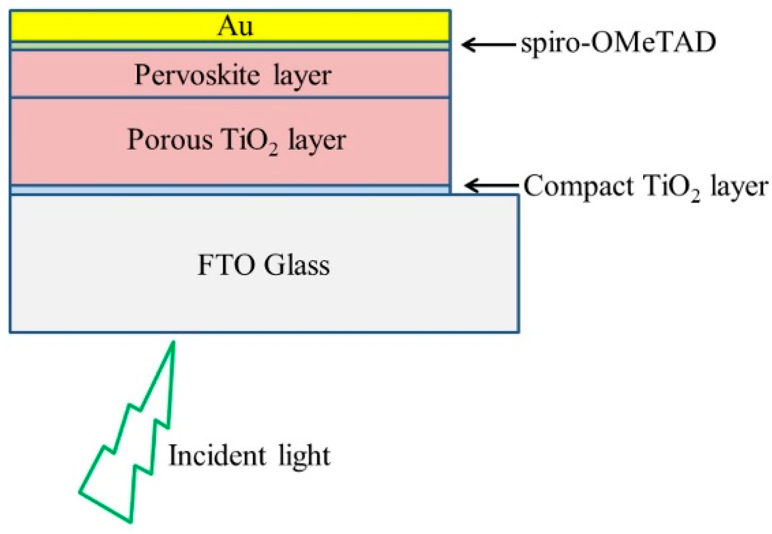
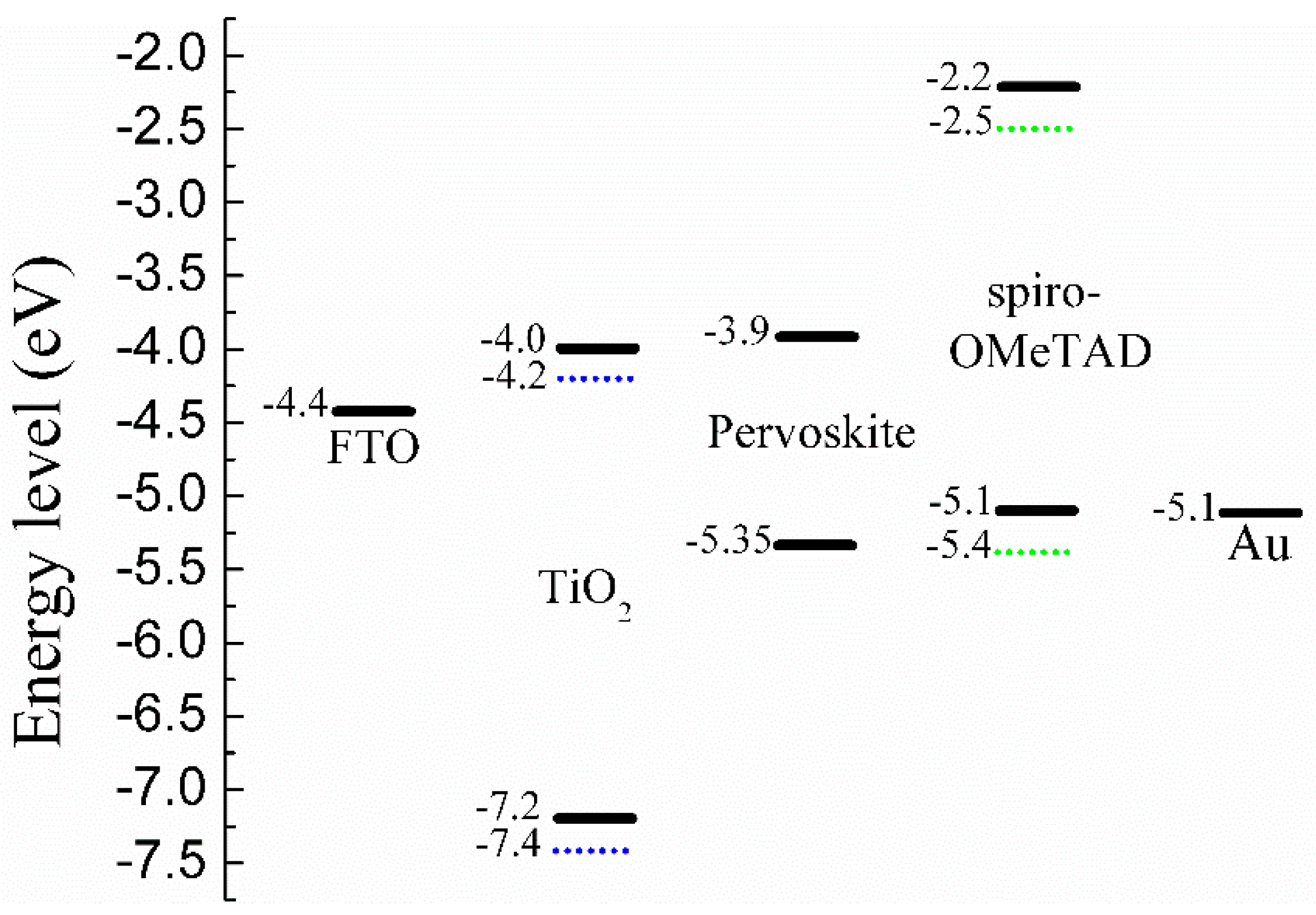
2.1. Solar Cell Structure for the Study

Fluorine-doped tin oxide (FTO) was adopted as front contact and thin layer of gold (Au) was used as back metal contact. The solar cell configuration for this study was FTO glass/compact TiO2/porous TiO2/perovskite absorber layer/spiro-OMeTAD/Au. In this n-i-p device structure, the perovskite layer acted as light harvesting material, inserted between n-type ETL (TiO2) and p-type HTL (spiro-OMeTAD). The solar cell structure is presented in Figure 1.

2.2. Simulation Methodology

The SCAPS-1D simulation software was selected for this study, which was developed by the University of Ghent, Belgium. The simulation calculation carried out inside SCAPS-1D is mainly derived from three fundamental equations: Poisson equation, electron continuity equation and hole continuity equation. In SCAPS-1D, a heterostructure solar cell can be designed with up to seven different layers and simulation can be performed in various variables about the electron and optics properties of the solar cell functional thin films.
The model was built by the SCAPS-1D with experimental parameters from the virtual ambient air fabricated PSC in structure of FTO glass/c-TiO2/m-TiO2/CH3NH3PbI3/spiro-OMeTAD/Au and other well-known published parameters [38,39,40,41]. The detail of the ambient air prepared PSC can be found in our published reference [38], and the Jsc, Voc, FF and efficiency of the ambient air prepared solar cell were 25.71 mA/cm2, 0.8000 V, 42.45% and 8.73%. The band gap of the ambient air prepared perovskite absorber layer together with the thickness of the thin films for modelling were taken from experimental results. The experimental parameters were adjusted slightly within the measurement error before they were used, to make the experimental and simulated solar cell performance parameters fit well with each other. Initial defect density of the perovskite absorber layer (Nt) was set at 1.000 × 1015 cm−3. The basic parameters used to perform the simulation were collected and listed in Table 1 [38,39,40,41]. Table 2 lists the contact parameters used in the simulation. Table 3 presents the defect density inside the absorber layer and at the interface of the device.
After the model mentioned above was built, the Nt was changed and its effect on the performance of the ambient air prepared PSC was further studied. Then, the thickness of several important functional thin films were further analyzed by the SCAPS-1D. Finally, the effect of energy-level alignment with varied Nt on the characteristics of ambient air prepared PSC was thoroughly investigated.

3. Results and Discussion

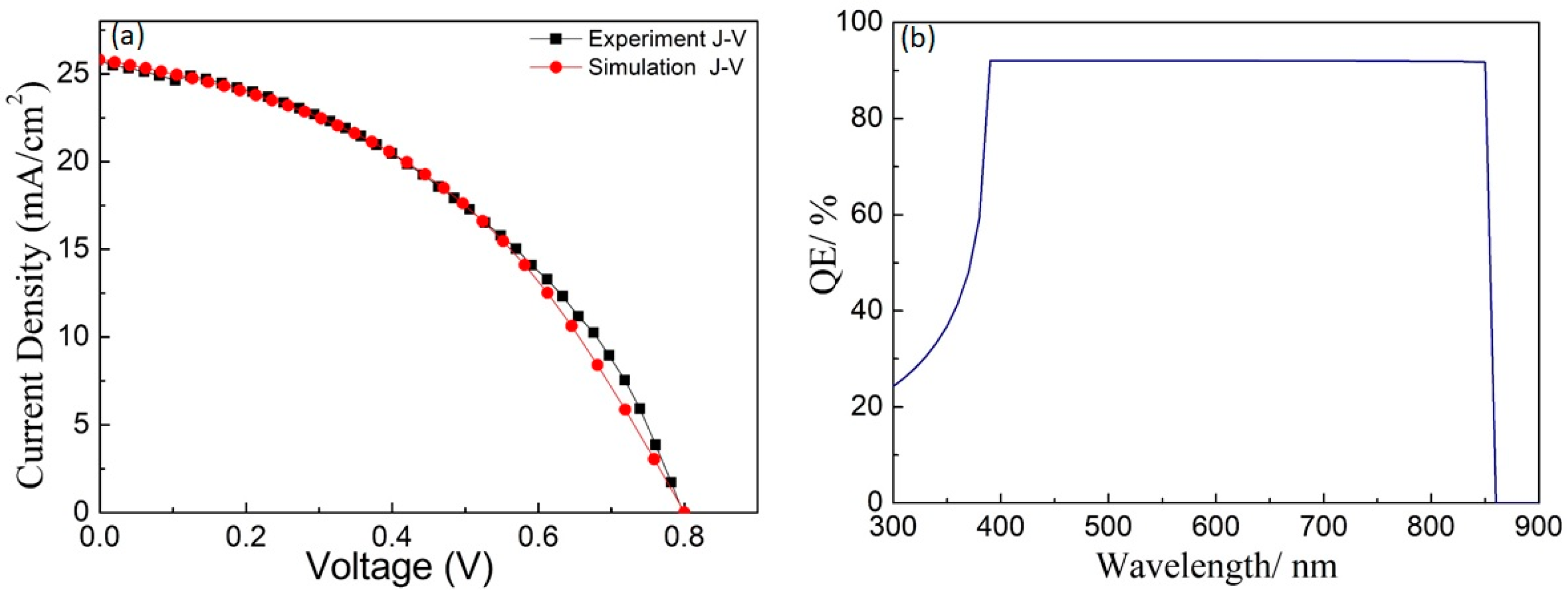
3.1. Fitting and Establishment of the Model

First, we carried out the fitting and establishment of the model for the PSC prepared in ambient air, as mentioned in Section 2. The band gap of the ambient air prepared perovskite absorber layer together with the thickness of the thin films for modelling were taken from the experimental results. The experimental parameters were adjusted slightly within the measurement error before they were used, to make the experimental and simulated solar cell performance parameters fit well with each other. The initial defect density of the perovskite absorber layer (Nt) was set at 1.000 × 1015 cm−3. The basic parameters used to perform the simulation are listed in Table 1. The results are in Figure 2a and Table 4. The QE result by the SCAPS is also displayed in Figure 2b.
As can be seen in Table 4 and Figure 2a, the Jsc, Voc, FF and efficiency of the prepared solar cell were 25.71 mA/cm2, 0.8000 V, 42.45% and 8.73%, respectively. The fitted Jsc, Voc, FF and efficiency from the model by the SCAPS-1D were 25.81 mA/cm2, 0.8001 V, 42.37% and 8.75%, respectively. The experimental and simulated performance parameters of the PSC fitted well with each other, which indicates the model is feasible. Figure 2b shows the QE result by the SCAPS, which indicates that the photon utilization efficiency of the PSC in the shortwave region of 300–400 nm was relatively low.

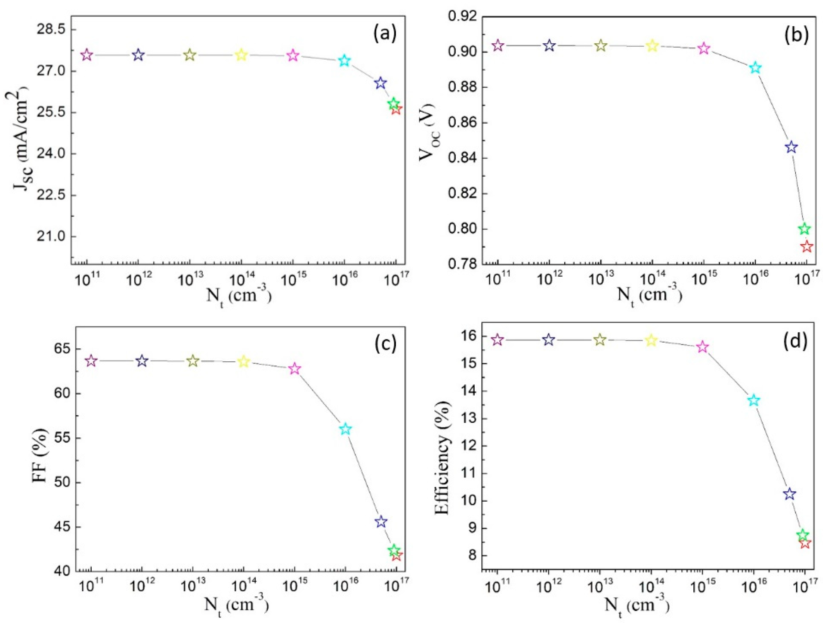
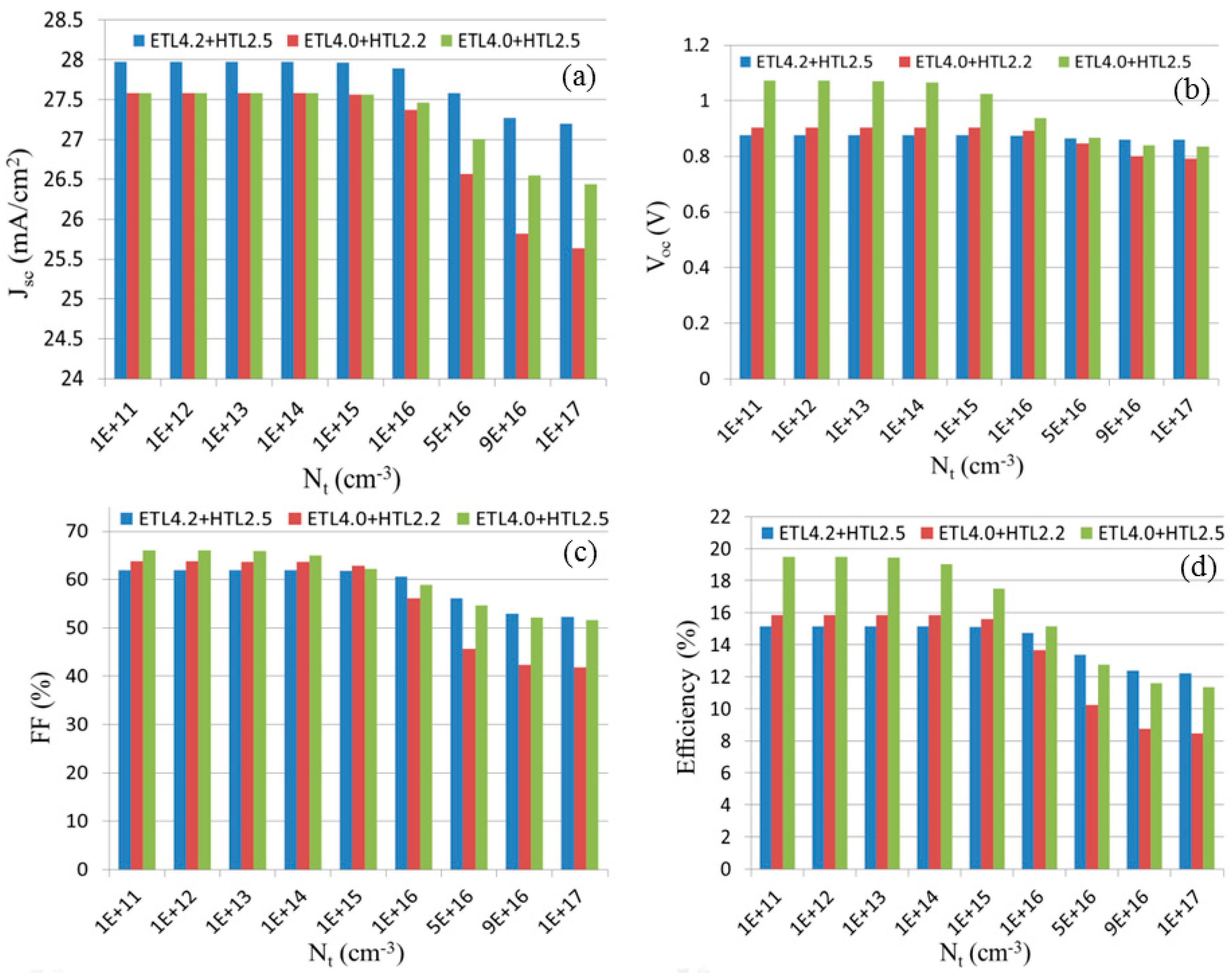
3.2. Effect of Defect Density (Nt) on the Performance of the Perovskite Solar Cell

As can be seen in Table 4, the Jsc of the ambient air prepared solar cell is considered to be high [42,43,44,45,46], however, the efficiency of the solar cell prepared in the ambient air is still limited by the low Voc and thus the low FF, which indicates the carrier recombination in the absorber layer and (ionic) defect recombination at the absorber layer/TL interfaces could be still serious [47]. The carrier recombination in the absorber layer could be the major recombination pathway in the prepared PSC, which can be confirmed from the simulation result that the defect density (Nt) of the perovskite absorber layer prepared in ambient air was very high to 9.000 × 1016 cm−3. Although the three-dimensional solar cell structure as mentioned in reference [38] can keep the Jsc high, the high Nt of the perovskite absorber layer directly pulls down the Voc of the solar cell and thus the FF and efficiency. In the Shockley–Read–Hall recombination that governs the absorber layer, the carriers in valence (holes) and conduction (electrons) bands recombine via trap states [48,49]. Therefore, by decreasing the defect density, less recombination in the absorber layer that corresponds to longer carrier diffusion length and larger carrier lifetime (tn and tp) could be realized [48,49]. This would be further studied in the following.
The performance of the solar cell with a varied Nt (1.000 × 10¹¹~1.000 × 1017 cm−3) of the perovskite absorber layer was carried out by using the SCAPS-1D simulator, and the results are shown in Figure 3. It can be seen from the Figure, the performance parameter Jsc slightly increased from 25.81 to 27.58 mA/cm2 as the Nt was improved from 9.000 × 10¹⁶ to 1.000 × 1011 cm−3. However, it reached near saturation when the Nt was improved to 1.000 × 1015 cm−3. Thus, in the prepared PSC, the Jsc was less dependent on the Nt of the perovskite absorber layer. Meanwhile, the value of the crucial parameter Voc was promoted significantly from 0.8001 to 0.9037 V as the Nt of the absorber layer was reduced from 9.000 × 10¹⁶ to 1.000 × 1011 cm−3, nearly a 13% improvement. The FF changed from 42.37 to 63.68%, which may have been due to the improved quality of the perovskite absorber layer with Nt from 1017 to 1011 cm−3. During this change process, there exists a near saturation phenomenon for the FF when Nt is improved to 1013 cm−3, which indicates that the Nt is good enough for solar cell application and is no longer the main influencing factor for solar cell performance. The efficiency of the solar cell was improved correspondingly from 8.75 to 15.87%. It is worth mentioning, the efficiencies of the solar cells reached 15.61% and 15.85% when the Nt of the absorber were at 1.000 × 1015 cm−3 and 1.000 × 1014 cm−3, which is easy to implement by experiment. The variation in carrier diffusion length of the absorber layer with the variation of Nt is also present in Table 5. As can be seen from the Table, the diffusion length of the carriers reached μm, and the carrier lifetime came to 200 nm when the Nt of the perovskite absorber layer was at 1.000 × 1015 cm−3. Therefore, for the ambient air prepared PSC, the Nt of the perovskite absorber layer could be a focus for work to further improve its performance.

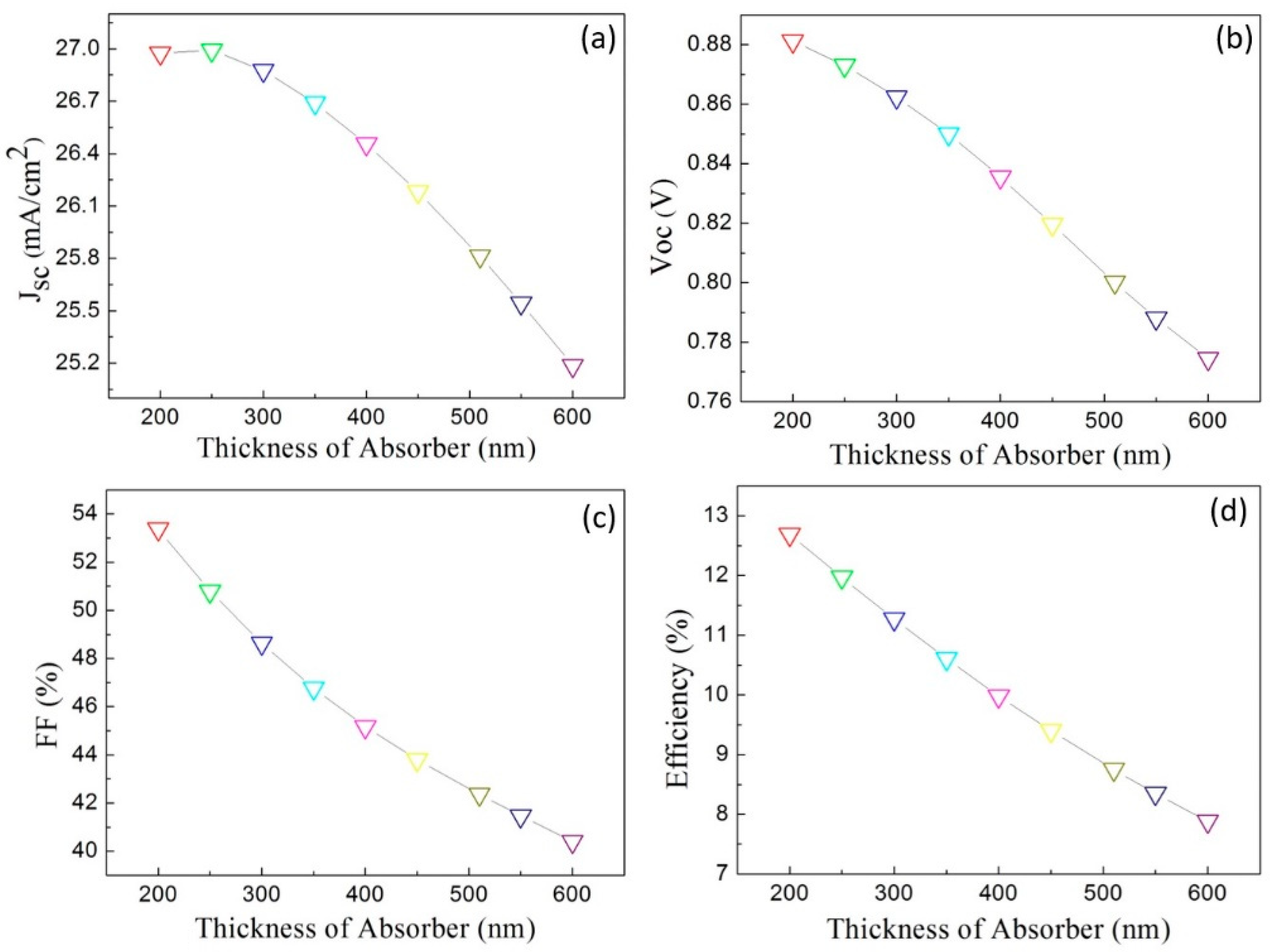
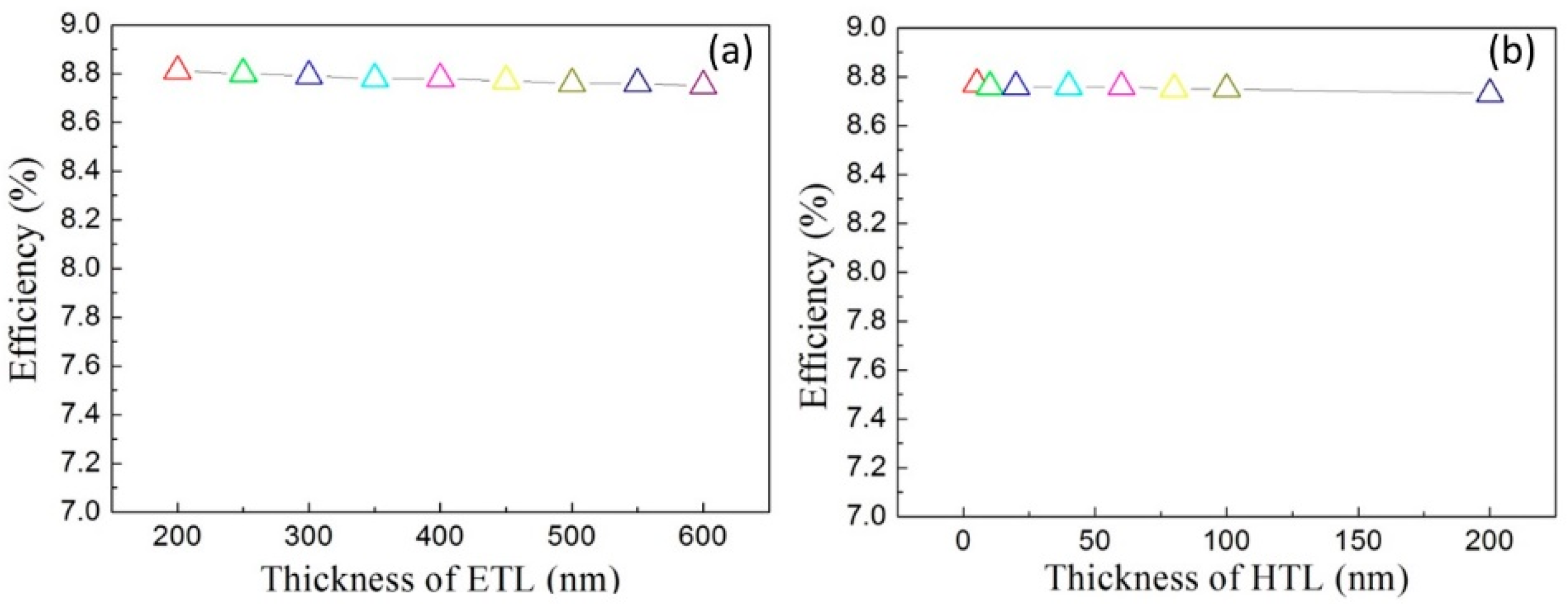
3.3. Thickness Effect of the Absorber Layer, ETL and HTL Layer on the Performance of the Perovskite Solar Cell

The thickness effects of the absorber layer, ETL and HTL layer on the performance of the PSC were studied by the SCAPS-1D and the results are displayed in Figure 4 and Figure 5, while keeping the Nt of the perovskite absorber layer at experimental value of 9.000 × 1016 cm−3. In the case of a variation in absorber layer thickness, we have taken all the basic parameters shown in Section 2. The absorber thickness was varied from 200 to 600 nm and the results are shown in Figure 4 for the required parameters, i.e., Jsc, Voc, FF and efficiency of the solar cell. It is depicted in Figure 4a–d that the Jsc slightly increased from 25.81 to 26.97 mA/cm2 as the thickness of the absorber was reduced from 600 to 200 nm. However, the Voc was increased from 0.8001 to 0.8812 V as the thickness of the absorber layer reduced from 600 to 200 nm, nearly 10% improvement. The FF was thus changed from 42.37 to 53.37%, the efficiency of the solar cell was improved from 8.75 to 12.69%. The change trend was similar to that mentioned in Section 3.2. Figure 5 presents the thickness effects of the ETL (200~600 nm) and HTL (5~200 nm) on the efficiency of the solar cell. As can be seen in the Figure, they had no significant impact on the performance of the solar cell.
The thickness effect of absorber, ETL and HTL could be important in the case of PSC heterostructures, as reported in the literature [50,51,52]. The results described above could be due to the high Nt of the perovskite absorber layer prepared in ambient air. Although, a thicker absorber is expected to absorb more incident light and therefore more carriers could be generated. The generated electron-hole pairs would be recombined easily in the absorber layer with high Nt. The decrement in FF is basically due to the internal recombination inside the perovskite material, originating from the short carrier lifetime of the electron (tn) and hole (tp) (just around 1.1 ns), as shown in Table 5. When the Nt of the perovskite absorber layer is high, the thickness effect of ETL and HTL is weakened, since internal recombination inside the perovskite absorber layer dominates the performance of solar cells. According to the results, when it is difficult to reduce the Nt of the absorber layer fabricated in ambient air technology, preparing a thin absorber layer could be a compromise choice to save material costs and, meanwhile, improve the efficiency of the PSC.

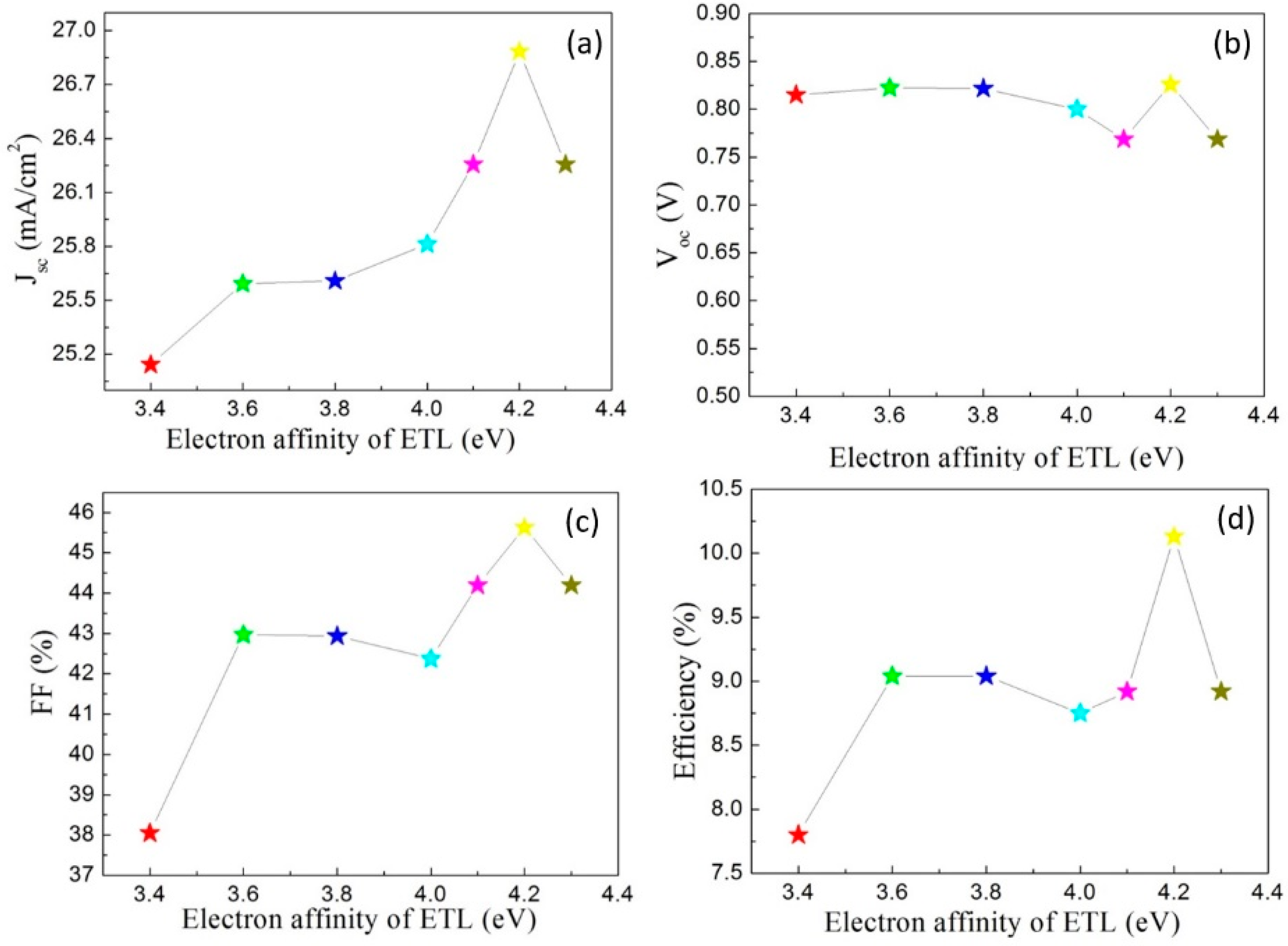
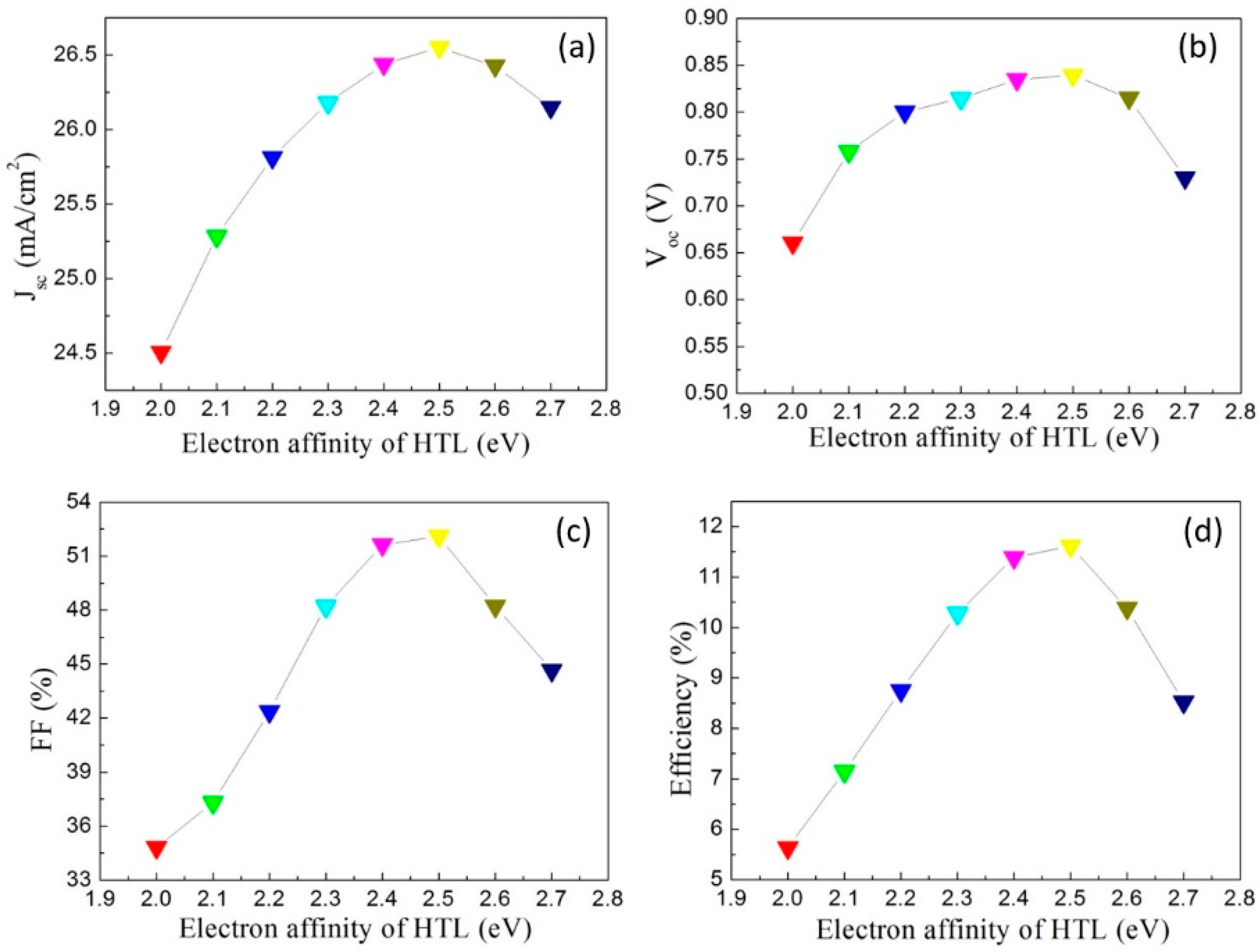
3.4. Effect of Electron Affinity of ETL and HTL Layer on the Performance of the Perovskite Solar Cell

The electron affinities of ETL and HTL set up the energy-level alignment between the absorber layer and the TLs, which could be significant for the efficiency of the PSC because they create interfaces for charge transport [25,53,54,55,56]. However, the underlying physical processes and loss characteristics of the energy-level alignment are still not clear. In particular, the dynamic influence characteristics of the energy-level alignment with a varied Nt has not been reported yet.
In the light of this, first, we checked the effect of the varied affinity of ETL (3.4–4.3 eV) and HTL (2.0–2.7 eV) on the performance of the PSC, while keeping the Nt of the perovskite absorber layer at the experimental value of 9.000 × 1016 cm−3. The values of Jsc, Voc, FF and the efficiency of the solar cell were recorded and plotted in Figure 6 for ETL when the electron affinity of HTL was kept at 2.2 eV, and in Figure 7 for HTL when the electron affinity of ETL was kept at 4.0 eV. It can be seen from Figure 6 that the Jsc, FF and efficiency increased when the electron affinity of ETL increased from 4.0 to 4.2 eV, which could be due to the more effective electron transport from the perovskite absorber layer to the ETL. However, when the electron affinity of ETL was further increased to 4.3 eV, the performance of the solar cell came down, which may be due to the energy-level mismatch between the absorber layer and the ETL for electron transport, while, from Figure 6b, we can see that the Voc did not present a significant change with the varied affinity of ETL from 3.4 to 4.3 eV. This phenomenon may be due to insufficient carriers under the high Nt of 9.000 × 1016 cm−3 that weakened the effect of energy-level matching between the absorber layer and the ETL on the Voc. In the condition of high Nt, the Jsc was the major influencing factor for the performance of PSC. The FF followed the change trend of the Jsc, and thus the efficiency of the PSC, as shown in Figure 6c,d. In the case of the HTL, it can be seen from Figure 7 that the Jsc, Voc, FF and efficiency decreased when the electron affinity of HTL decreased from 2.2 to 2.0 eV, which could be due to the gradually decreased efficiency in hole transport from the perovskite absorber layer to the HTL (energy gap of the valence band between these two layers is increased gradually). In contrast, when increasing the electron affinity of the HTL from 2.2 to 2.5 eV, the performance of the solar cell showed significant improvement, which may be due tothe better energy level between the absorber layer and the HTL for the hole transport [57,58,59]. However, when the electron affinity of the HTL was further increased to 2.7 eV, the energy level between the absorber layer and the HTL for the hole transport showed an obvious mismatch, and the performance of the solar cell came down sharply. In the HTL case, at a condition of high Nt, the Jsc was still the major influencing factor for the performance of PSC. Yet, it is worth noting that in Figure 7, the performance reached the top when the electron affinity of the HTL was at 2.5 eV, which made the valence band of the HTL 0.05 eV lower than that of the perovskite absorber layer and this usually would hinder the hole transport to a certain degree. This could be an unusual phenomenon and would be studied further in the following paragraphs.
In order to further understand the effect of energy-level matching between the ETL, perovskite absorber layer and HTL on the performance of the PSC, three groups of electron affinity of ETL and HTL, named “ETL(4.2)+HTL(2.5)” (electron affinities of ETL and HTL were 4.2 eV and 2.5 eV, respectively), “ETL(4.0)+HTL(2.2)” (electron affinities of ETL and HTL were 4.0 eV and 2.2 eV, respectively) and “ETL(4.0)+HTL(2.5)” (electron affinities of ETL and HTL were 4.0 eV and 2.5 eV, respectively), were studied with the varied Nt of the perovskite absorber layer. The energy-level diagram of the ETL, the perovskite absorber layer and the HTL, including the three cases is shown in Figure 8, and the corresponding performance of the solar cell is presented in Figure 9. As can be seen from Figure 9a, for all three cases, the Jsc increased with the improvement of the Nt of the perovskite absorber layer because of reduced carrier recombination and therefore more electrons and holes could be extracted. However, they had different characteristics between the three cases. When at a high Nt value, there were not so many carriers available, the effect of the energy-level matching was obvious. In this situation, the normal “ETL(4.0)+HTL(2.2)” was not good enough, and the Jsc would be enhanced when the electron affinity of the HTL was increased to 2.5 eV, resulting in the valence band of the HTL 0.05 eV being lower than that of the perovskite absorber layer. This could have benefitted from the blocking effect that reduced the carrier recombination from the Au electrode to the perovskite absorber layer. The effect could be further enhanced by increasing the electron affinity of the ETL to 4.2 eV, which made the electron transport from the absorber layer to the ETL easier. As for the Voc shown in Figure 9b, when at high Nt, it did not make a big difference between the three cases. However, when the Nt of the absorber layer was improved, the energy-level matching became important. In the “ETL(4.0)+HTL(2.5)” case, although it was not the best combination for the Jsc of the solar cell, it presented minimum loss between the three cases for the Voc since it matched well with the QFLS in the perovskite absorber layer under light illumination [25]. As for the parameter FF, it generally followed the Jsc, and was also affected by Voc, as can be observed in Figure 9c. Since the efficiency of the solar cell equals the product of Jsc, Voc and FF, hence, the efficiency is affected by the evident Voc to a greater extent, as can be seen from Figure 9. Therefore, the effect of energy-level matching on the performance of the PSC is affected by the Nt, and the energy-level matching between the ETL and the perovskite absorber layer produces a counterbalancing characteristic on Jsc and Voc at improved Nt. When the Nt of the absorber layer is at 1.000 × 1011 cm−3, the “ETL(4.0)+HTL(2.5)” case can push the solar cell to high performance with a Jsc of 27.58 m A/cm2, Voc of 1.0713V, FF of 66.02% and efficiency of 19.51%.

4. Conclusions

In this study, a model for a PSC prepared in ambient air was established by employing the SCAPS-1D. Then, the model was analyzed with a varying of the Nt of the perovskite absorber layer, the thickness of the absorber, ETL and HTL, and finally the electron affinity of ETL and HTL. It was found that (1) the Nt of the perovskite absorber layer is very important for the performance of the solar cell, especially for the Voc; (2) when at a high Nt for the perovskite absorber layer prepared in ambient air, the absorber layer could be prepared thinner (such as 200 nm) to reduce the carrier transport distance, in order to reduce recombination. This would overcome the defect of the high Nt to a certain degree, although a thin absorber layer decreases the absorption of the incident light. When the Nt is high, the thickness effect of the ETL and HTL is weakened, since internal recombination inside the perovskite absorber layer dominates the performance of the solar cells; (3) the electron affinities of ETL and HTL could be significant for the performance of the solar cell. It was found that the HTL with a valence band 0.05 eV lower than that of the perovskite absorber layer could have a blocking effect that reduced the carrier recombination from the Au electrode to the perovskite absorber layer. The effect could be further enhanced by reducing the conduction band energy of the ETL to −4.2 eV, which made the electron transport from the absorber layer to ETL more easily. As for Voc, at high Nt, it did not make a big difference between the three studied cases. However, when the Nt of the absorber layer was improved, the energy-level matching became important. In the “ETL(4.0)+HTL(2.5)” situation it presented a minimum Voc loss between the three cases since it matched well with the quasi-Fermi level splitting (QFLS) of the perovskite absorber layer under light illumination. For the parameter FF, it generally followed the Jsc, and was also affected by Voc. The efficiency of the solar cell was more affected by the evident Voc. Therefore, the effect of energy-level matching on the performance of the PSC is affected by the Nt, and the energy-level matching between the ETL and the perovskite absorber layer has a counterbalancing characteristic on the Jsc and Voc at improved Nt. When the Nt of the absorber layer was at 1.000 × 1014 cm−3 and 1.000 × 1015 cm−3, which were easy to achieve by the experimental route, the “ETL(4.0)+HTL(2.5)” case resulted in efficiencies of 17.53% and 19.06%, respectively. The solar cell exhibited an efficiency of 19.51% with Jsc of 27.58 mA/cm2, Voc of 1.0713 V and FF of 66.02% when Nt was at 1.000 × 1011 cm−3. This study may contribute to the improvement of the PSC in the optimization of defect density, thin film thickness and energy-level balance.

Author Contributions

Conceptualization, Q.C. and X.D.; methodology, Q.C. and Y.N.; formal analysis, Q.C., Y.N. and Y.Y.; investigation, Q.C., Y.N. and X.D.; writing—original draft preparation, Q.C.; writing—review and editing, Y.N., X.D. and Y.Y.; project administration, Q.C.; funding acquisition, Q.C. All authors have read and agreed to the published version of the manuscript.

Funding

The project was supported by the National Natural Science Foundation of China (No. 11604097).

Institutional Review Board Statement

Not applicable.

Informed Consent Statement

Not applicable.

Data Availability Statement

Not applicable.

Acknowledgments

The authors would like to acknowledge Burgelman’s group from University of Ghent, Belgium for providing the SCAPS simulator.

Conflicts of Interest

The authors declare no conflict of interest.

References

  1. Kojima, A.; Teshima, K.; Shirai, Y.; Miyasaka, T. Organometal Halide Perovskites as Visible-Light Sensitizers for Photovoltaic Cells. J. Am. Chem. Soc. 2009, 131, 6050–6051. [Google Scholar] [CrossRef]
  2. Stranks, S.D.; Eperon, G.E.; Grancini, G.; Menelaou, C.; Alcocer, M.J.P.; Leijtens, T.; Herz, L.M.; Petrozza, A.; Snaith, H.J. Electron-Hole Diffusion Lengths Exceeding 1 Micrometer in an Organometal Trihalide Perovskite Absorber. Science 2013, 342, 341–344. [Google Scholar] [CrossRef] [Green Version]
  3. Ahmed, S.; Jannat, F.; Khan, M.A.K.; Alim, M.A. Numerical development of eco-friendly Cs2TiBr6 based perovskite solar cell with all-inorganic charge transport materials via SCAPS-1D. Optik 2021, 225, 165765. [Google Scholar] [CrossRef]
  4. Santos, I.M.D.L.; Cortina-Marrero, H.J.; Ruíz-Sánchez, M.A.; Hechavarría-Difur, L.; Sánchez-Rodríguez, F.J.; Courel, M.; Hu, H. Optimization of CH3NH3PbI3 perovskite solar cells: A theoretical and experimental study. Sol. Energy 2020, 199, 198–205. [Google Scholar] [CrossRef]
  5. Singh, S.; Laxmi; Kabra, D. Defects in halide perovskite semiconductors: Impact on photo-physics and solar cell performance. J. Phys. D Appl. Phys. Superlattices Microstruct. 2020, 53, 503003. [Google Scholar] [CrossRef]
  6. Burschka, J.; Pellet, N.; Moon, S.J.; Humphry-Baker, R.; Gao, P.; Nazeeruddin, M.K.; Grätzel, M. Sequential Deposition as a Route to High-Performance Perovskite-Sensitized Solar Cells. Nature 2013, 499, 316–319. [Google Scholar] [CrossRef] [PubMed]
  7. Jeon, N.J.; Noh, J.H.; Kim, Y.C.; Yang, W.S.; Ryu, S.; Seok, S.I. Solvent engineering for high-performance inorganic–organic hybrid perovskite solar cells. Nat. Mater. 2014, 13, 897–903. [Google Scholar] [CrossRef]
  8. Snaith, H.J. Present status and future prospects of perovskite photovoltaics. Nat. Mater. 2018, 17, 372–376. [Google Scholar] [CrossRef]
  9. Rong, Y.; Hu, Y.; Mei, A.; Tan, H.; Saidaminov, M.I.; Seok, S.I.; McGehee, M.D.; Sargent, E.H.; Han, H. Challenges for commercializing perovskite solar cells. Science 2018, 361, eaat8235. [Google Scholar] [CrossRef] [Green Version]
  10. Cheng, Z.; Lin, J. Layered organic–inorganic hybrid perovskites: Structure, optical properties, film preparation, patterning and templating engineering. CrystEngComm 2010, 12, 2646–2662. [Google Scholar] [CrossRef]
  11. Jung, E.H.; Jeon, N.J.; Park, E.Y.; Moon, C.S.; Shin, T.J.; Yang, T.Y.; Noh, J.H.; Seo, J.W. Efficient, stable and scalable perovskite solar cells using poly(3-hexylthiophene). Nature 2019, 567, 511–515. [Google Scholar] [CrossRef]
  12. Available online: https://www.nrel.gov/pv/cell-efficiency.html (accessed on 7 December 2021).
  13. Ashraf, M.A.; Alam, I. Numerical simulation of CIGS, CISSe and CZTS-based solar cells with In2S3 as buffer layer and Au as back contact using SCAPS 1D. Eng. Res. Express 2020, 2, 035015. [Google Scholar] [CrossRef]
  14. Uliná, S.; Welch, L.M.; Abbas, A.; Togay, M.; Tsai, V.; Betts, T.R.; Malkov, A.V.; Walls, J.M.; Bowers, J.W. Sodium doping of solution-processed amine-thiol based CIGS solar cells by thermal evaporation of NaCl. Prog. Photov. Res. Appl. 2021, 29, 546–557. [Google Scholar] [CrossRef]
  15. Ablekim, T.; Duenow, J.N.; Zheng, X.; Moutinho, H.; Metzger, W.K. Thin film solar cells with 19% efficiency by thermal evaporation of CdSe and CdTe. ACS Energy Lett. 2022, 5, 892–896. [Google Scholar] [CrossRef]
  16. Krückemeier, L.; Rau, U.; Stolterfoht, M.; Kirchartz, T. How to Report Record Open-Circuit Voltages in Lead-Halide Perovskite Solar Cells. Adv. Energy Mater. 2020, 10, 1902573. [Google Scholar] [CrossRef]
  17. Tress, W. Perovskite Solar Cells on the Way to Their Radiative Efficiency Limit-Insights Into a Success Story of High Open-Circuit Voltage and Low Recombination. Adv. Energy Mater. 2017, 7, 1602358. [Google Scholar] [CrossRef]
  18. Shi, D.; Adinolfi, V.; Comin, R.; Yuan, M.; Alarousu, E.; Buin, A.; Chen, Y.; Hoogland, S.; Rothenberger, A.; Katsiev, K.; et al. Low trap-state density and long carrier diffusion in organo lead trihalide perovskite single crystals. Science 2015, 347, 519–522. [Google Scholar] [CrossRef] [Green Version]
  19. Yang, Y.; Yang, M.; Moore, D.T.; Yan, Y.; Miller, E.M.; Zhu, K.; Beard, M.C. Top and Bottom Surfaces Limit Carrier Lifetime in Lead Iodide Perovskite Films. Nat. Energy 2017, 2, 16207. [Google Scholar] [CrossRef]
  20. Zheng, X.; Chen, B.; Dai, J.; Fang, Y.; Bai, Y.; Lin, Y.; Wei, H.; Zeng, X.C.; Huang, J. Defect passivation in hybrid perovskite solar cells using quaternary ammonium halide anions and cations. Nat. Energy 2017, 2, 17102. [Google Scholar] [CrossRef]
  21. Son, D.Y.; Lee, J.W.; Choi, Y.J.; Jang, I.H.; Lee, S.; Yoo, P.J.; Shin, H.; Ahn, N.; Choi, M.; Kim, D.; et al. Self-formed grain boundary healing layer for highly efficient CH3NH3PbI3 perovskite solar cells. Nat. Energy 2016, 1, 16081. [Google Scholar] [CrossRef]
  22. Abdi-Jalebi, M.; Andaji-Garmaroudi, Z.; Cacovich, S.; Stavrakas, C.; Philippe, B.; Richter, J.M.; Alsari, M.; Booker, E.P.; Hutter, E.M.; Pearson, A.J.; et al. Maximizing and stabilizing luminescence from halide perovskites with potassium passivation. Nature 2018, 555, 497–501. [Google Scholar] [CrossRef] [PubMed]
  23. Stolterfoht, M.; Wolff, C.M.; Ma´rquez, J.A.; Zhang, S.; Hages, C.J.; Rothhardt, D.; Albrecht, S.; Burn, P.L.; Meredith, P.; Unold, T.; et al. Visualization and suppression of interfacial recombination for high-efficiency large-area pin perovskite solar cells. Nat. Energy 2018, 3, 847–854. [Google Scholar] [CrossRef]
  24. Sarritzu, V.; Sestu, N.; Marongiu, D.; Chang, X.; Masi, S.; Rizzo, A.; Colella, S.; Quochi, F.; Saba, M.; Mura, A.; et al. Optical determination of Shockley-Read-Hall and interface recombination currents in hybrid perovskites. Sci. Rep. 2017, 7, 44629. [Google Scholar] [CrossRef] [PubMed] [Green Version]
  25. Stolterfoht, M.; Caprioglio, P.; Wolff, C.M.; Márquez, J.A.; Nordmann, J.; Zhang, S.; Rothhardt, D.; Hrmann, U.; Amir, Y.; Redinger, A. The impact of energy alignment and interfacial recombination on the internal and external open-circuit voltage of perovskite solar cells. Energy Environ. Sci. 2019, 12, 2778–2788. [Google Scholar] [CrossRef] [Green Version]
  26. Wolff, C.M.; Zu, F.; Paulke, A.; Toro, L.P.; Koch, N.; Neher, D. Reduced interface-mediated recombination for high open-circuit voltages in CH3NH3PbI3 solar cells. Adv. Mater. 2017, 29, 1700159. [Google Scholar] [CrossRef] [PubMed]
  27. Schulz, P.; Edri, E.; Kirmayer, S.; Hodes, G.; Cahen, D.; Kahn, A. Interface energetics in organo-metal halide perovskite-based photovoltaic cells. Energy Environ. Sci. 2014, 7, 1377–1381. [Google Scholar] [CrossRef]
  28. Polander, L.E.; Pahner, P.; Schwarze, M.; Saalfrank, M.; Koerner, C.; Leo, K. Hole-transport material variation in fully vacuum deposited perovskite solar cells. APL Mater. 2014, 2, 081503. [Google Scholar] [CrossRef] [Green Version]
  29. Gelmetti, I.; Montcada, N.F.; Pérez-Rodríguez, A.; Barrena, E.; Ocal, C.; García-Benito, I.; Molina-Ontoria, A.; Martín, N.; Vidal-Ferran, A.; Palomares, E. Energy alignment and recombination in perovskite solar cells: Weighted influence on the open circuit voltage. Energy Environ. Sci. 2019, 12, 1309–1316. [Google Scholar] [CrossRef]
  30. Belisle, R.A.; Jain, P.; Prasanna, R.; Leijtens, T.; McGehee, M.D. Minimal Effect of the Hole-Transport Material Ionization Potential on the Open-Circuit Voltage of Perovskite Solar Cells. ACS Energy Lett. 2016, 1, 556–560. [Google Scholar] [CrossRef]
  31. Guo, Q.; Yuan, F.; Zhang, B.; Zhou, S.; Zhang, J.; Bai, Y.; Fan, L.; Hayat, T.; Alsaedi, A.; Tan, Z.A. Passivation of the grain boundaries of CH3NH3PbI3 using carbon quantum dots for highly efficient perovskite solar cells with excellent environmental stability. Nanoscale 2019, 11, 115–124. [Google Scholar] [CrossRef] [PubMed]
  32. Li, H.; Zhu, K.; Zhang, K.; Huang, P.; Li, D.; Yuan, L.; Cao, T.; Sun, Z.; Li, Z.; Chen, Q.; et al. 3,4-Dihydroxybenzhydrazide as an additive to improve the morphology of perovskite films for efficient and stable perovskite solar cells. Org. Electron. 2019, 66, 47–52. [Google Scholar] [CrossRef]
  33. Yang, Z.; Pan, J.; Liang, Y.; Li, Q.; Xu, D. Ambient Air Condition for Room-Temperature Deposition of MAPbI3 Films in Highly Efficient Solar Cells. Small 2018, 14, 1802240. [Google Scholar] [CrossRef]
  34. Moyez, S.A.; Roy, S. Dual-step thermal engineering technique: A new approach for fabrication of efficient CH3NH3PbI3-based perovskite solar cell in open air condition. Sol. Energy Mater. Sol. Cells 2018, 185, 145–152. [Google Scholar] [CrossRef]
  35. Nia, N.Y.; Zendehdel, M.; Cinà, L.; Matteocci, F.; Carlo, A.D. A crystal engineering approach for scalable perovskite solar cells and module fabrication: A full out of glove box procedure. J. Mater. Chem. A 2018, 6, 659–671. [Google Scholar]
  36. Troughton, J.; Charbonneau, C.; Carnie, M.J.; Davies, M.L.; Worsley, D.A.; Watson, T.M. Rapid processing of perovskite solar cells in under 2.5 seconds. J. Mater. Chem. A 2015, 3, 9123–9127. [Google Scholar] [CrossRef]
  37. Huang, Y.C.; Li, C.F.; Huang, Z.H.; Liu, P.H.; Tsao, C.S. Rapid and sheet-to-sheet slot-die coating manufacture of highly efficient perovskite solar cells processed under ambient air. Sol. Energy 2019, 177, 255–261. [Google Scholar] [CrossRef]
  38. Zhu, W.; Chen, Q.M.; Yamaguchi, Y.; Zhao, F.; Hao, D.C.; Liu, X.H.; Dou, X.M. Perovskite solar cells prepared under infrared irradiation during fabrication process in air ambience. J Mater. Sci. Mater. Electron. 2020, 31, 9535–9542. [Google Scholar] [CrossRef]
  39. Caprioglio, P.; Wolff, C.M.; Sandberg, O.J.; Armin, A.; Stolterfoht, M. On the Origin of the Ideality Factor in Perovskite Solar Cells. Adv. Energy Mater. 2020, 10, 2000502. [Google Scholar] [CrossRef]
  40. Sandberg, O.J.; Kurpiers, J.; Stolterfoht, M.; Neher, D.; Meredith, P.; Shoaee, S.; Armin, A. On the Question of the Need for a Built-In Potential in Perovskite Solar Cells. Adv. Mater. Interfaces 2020, 7, 2000041. [Google Scholar] [CrossRef] [Green Version]
  41. Caprioglio, P.; Stolterfoht, M.; Wolff, C.M.; Unold, T.; Rech, B.; Albrecht, S.; Neher, D. On the Relation between the Open-Circuit Voltage and Quasi-Fermi Level Splitting in Efficient Perovskite Solar Cells. Adv. Energy Mater. 2019, 9, 1901631. [Google Scholar] [CrossRef] [Green Version]
  42. Nanu, M.; Schoonman, J.; Goossens, A. Nanocomposite Three-Dimensional Solar Cells Obtained by Chemical Spray Deposition. Nano Lett. 2005, 5, 1716–1719. [Google Scholar] [CrossRef]
  43. Nanu, M.; Schoonman, J.; Goossens, A. Inorganic Nanocomposites of n- and p-Type Semiconductors: A New Type of Three-Dimensional Solar Cell. Adv. Mater. 2004, 16, 453–456. [Google Scholar] [CrossRef]
  44. Guldin, S.; Hüttner, S.; Kolle, M.; Welland, M.E.; Müller-Buschbaum, P.; Friend, R.H.; Steiner, U.; Tétreault, N. Dye-Sensitized Solar Cell Based on a Three-Dimensional Photonic Crystal. Nano Lett. 2010, 10, 2303–2309. [Google Scholar] [CrossRef] [PubMed] [Green Version]
  45. van Bavel, S.S.; Sourty, E.; de With, G.; Loos, J. Three-Dimensional Nanoscale Organization of Bulk Heterojunction Polymer Solar Cells. Nano Lett. 2009, 9, 507–513. [Google Scholar] [CrossRef]
  46. Xiao, Z.; Dong, Q.; Bi, C.; Shao, Y.; Yuan, Y.; Huang, J. Solvent Annealing of Perovskite-Induced Crystal Growth for Photovoltaic-Device Efficiency Enhancement. Adv. Mater. 2014, 26, 6503–6509. [Google Scholar] [CrossRef]
  47. Ameri, M.; Ghaffarkani, M.; Ghahrizjani, R.T.; Safari, N.; Mohajerani, E. Phenomenological morphology design of hybrid organic-inorganic perovskite solar cell for high efficiency and less hysteresis. Sol. Energy Mater. Sol. Cells 2020, 205, 110251. [Google Scholar] [CrossRef]
  48. Sherkar, T.S.; Momblona, C.; Gil-Escrig, L.; Avila, J.; Sessolo, M.; Bolink, H.J.; Koster, L.J.A. Recombination in perovskite solar cells: Significance of grain boundaries, interfacetraps, and defect ions. ACS Energy Lett. 2017, 2, 1214–1222. [Google Scholar] [CrossRef]
  49. Zekry, A.; Shaker, A.; Salem, M. Chapter 1-solar cells and arrays: Principles, analysis, and design. In Advances in Renewable Energies and Power Technologies; Yahyaoui, I., Ed.; Elsevier: Amsterdam, The Netherlands, 2018; pp. 3–56. [Google Scholar]
  50. Kumar, M.; Raj, A.; Kumar, A.; Anshul, A. An optimized lead-free formamidinium Sn-based perovskite solar cell design for high power conversion efficiency by SCAPS simulation. Opt. Mater. 2020, 108, 110213. [Google Scholar] [CrossRef]
  51. Chowdhury, M.S.; Shahahmadi, S.A.; Chelvanathan, P.; Tiong, S.K.; Suklueng, M. Effect of Deep-Level Defect Density of the Absorber Layer and n/i Interface in Perovskite Solar Cells by SCAPS-1D. Results Phys. 2019, 16, 102839. [Google Scholar] [CrossRef]
  52. Abdelaziz, S.; Zekry, A.; Shaker, A.; Abouelatta, M. Investigating the performance of formamidinium tin-based perovskite solar cell by SCAPS device simulation. Opt. Mater. 2020, 101, 109738. [Google Scholar] [CrossRef]
  53. Wang, Q.; Mosconi, E.; Wolff, C.; Li, J.M.; Neher, D.; Angelis, F.D.; Paolo, G.; Roberto, S.; Abate, G.A. Rationalizing the Molecular Design of Hole-Selective Contacts to Improve Charge Extraction in Perovskite Solar Cells. Adv. Energy Mater. 2019, 9, 1900990. [Google Scholar] [CrossRef]
  54. Hima, A.; Lakhdar, N.; Benhaoua, B.; Saadoune, A.; Kemerchou, I.; Rogti, F. An optimized perovskite solar cell designs for high conversion efficiency. Superlattices Microstruct. 2019, 129, 240–246. [Google Scholar] [CrossRef]
  55. Rai, S.; Pandey, B.K.; Dwivedi, D.K. Modeling of highly efficient and low cost CH3NH3Pb(I1−xClx)3 based perovskite solar cell by numerical simulation. Opt. Mater. 2020, 100, 109631. [Google Scholar] [CrossRef]
  56. Burgelman, M.; Nollet, P.; Degrave, S. Modelling polycrystalline semiconductor solar cells. Thin Solid Film. 2000, 361–362, 527–532. [Google Scholar] [CrossRef]
  57. Azadinia, M.; Ameri, M.; Ghahrizjni, R.T.; Fathollahi, M. Maximizing the performance of single and multijunction MA and lead-free perovskite solar cell. Mater. Today Energy 2021, 20, 100647. [Google Scholar] [CrossRef]
  58. Shariatinia, Z. Recent progress in development of diverse kinds of hole transport materials for the perovskite solar cells: A review. Renew. Sust. Energy Rev. 2020, 119, 109608. [Google Scholar] [CrossRef]
  59. Kung, P.K.; Li, M.H.; Lin, P.Y.; Chiang, Y.H.; Chan, C.R. A Review of Inorganic Hole Transport Materials for Perovskite Solar Cells. Adv. Mater. Interfaces 2018, 5, 1800882. [Google Scholar] [CrossRef]
Figure 1. Device configuration of the perovskite solar cell.
Crystals 12 00068 g001
Figure 2. (a) The experimental and theoretical J-V curves of the PSC, (b) the QE result from the SCAPS.
Crystals 12 00068 g002
Figure 3. Effect of Nt of the perovskite on the (a) Jsc, (b) Voc, (c) FF and (d) efficiency of the solar cell.
Crystals 12 00068 g003
Figure 4. Thickness effect of the absorber layer on the (a) Jsc, (b) Voc, (c) FF and (d) efficiency of the solar cell.
Crystals 12 00068 g004
Figure 5. Thickness effect of (a) ETL and (b) HTL on the efficiency of the solar cell.
Crystals 12 00068 g005
Figure 6. Effect of electron affinity of ETL on the (a) Jsc, (b) Voc, (c) FF and (d) efficiency of the solar cell.
Crystals 12 00068 g006
Figure 7. Effect of electron affinity of HTL on (a) Jsc, (b) Voc, (c) FF and (d) efficiency of the solar cell.
Crystals 12 00068 g007
Figure 8. Energy-level diagram of the perovskite solar cell.
Crystals 12 00068 g008
Figure 9. Effect of electron affinity of the TL on the (a) Jsc, (b) Voc, (c) FF and (d) efficiency of the solar cell.
Crystals 12 00068 g009
Table 1. Physical parameters of different layers used for the simulation.
ParametersPerovskiteFTOTiO2Spiro-OMeTAD
Thickness (nm)51025060080
Band gap (eV)1.453.5003.202.90
Electron affinity (eV)3.904.4004.002.20
Dielectric permittivity22.009.000100.003.00
CB effective density of states (cm−3)3.100 × 10182.200 × 10181.000 × 10202.500 × 1020
VB effective density (cm−3)3.100 × 10181.800 × 10192.000 × 10202.500 × 1020
Electron thermal velocity (cm/S)1.000 × 1071.000 × 1071.000 × 1071.000 × 107
Hole thermal velocity (cm/s)1.000 × 1071.000 × 1071.000 × 1071.000 × 107
Electron mobility (cm2/Vs)102.000 × 103751.000 × 10−4
Hole mobility (cm2/Vs)101.000 × 102501.000 × 10−4
Shallow uniform donor density (ND, cm−3)1.000 × 10152.000 × 10191.000 × 10190
Shallow uniform acceptor density (NA, cm−3)1.000 × 1015001.000×1019
Table 2. Contact parameters used in the simulation.
ContactsBack Metal Contact PropertiesFront Metal Contact Properties
Metal work function (eV)5.104.06
Surface recombination velocity of electron (cm/s)1.000 × 1071.000 × 107
Surface recombination velocity of hole (cm/s)1.000 × 1071.000 × 107
Table 3. Defect density inside the absorber layer and at interface of the device.
ParameterAbsorberETL/AbsorberAbsorber/HTL
Defect densityNeutralNeutralNeutral
Capture cross section for electron (cm−2)1.000 × 10–151.000 × 10−102.000 × 10⁻¹⁵
Capture cross section for hole (cm−2)1.000 × 10–152.000 × 10−151.000 × 10⁻¹⁰
Energetic distributionSingleSingleSingle
Energy level with respect to Ev0.600.600.60
Characteristic energy (eV)NANANA
Table 4. Comparison of performance parameters of the experiment and simulation results.
ParameterExperimentSimulation
Jsc (mA/cm2)25.7125.81
Voc (V)0.80000.8001
FF (%)42.4542.37
Efficiency (%)8.738.75
Table 5. Variation in carrier diffusion length of the absorber layer according to variation in defect density (Nt).
Nt (cm−3)1.000 × 10179.000 × 10165.000 × 10161.000 × 10161.000 × 10151.000 × 10141.000 × 10131.000 × 10121.000 × 1011
Diffusion Length, L (μm)1.600 × 10−11.700 × 10−12.300 × 10−15.100 × 10−11.6005.1001.600 × 1015.100 × 1011.600 × 102
Lifetime, τn,p (ns)1.0001.1002.0001.000 × 1011.000 × 1021.000 × 1031.000 × 1041.000 × 1051.000 × 106
Publisher’s Note: MDPI stays neutral with regard to jurisdictional claims in published maps and institutional affiliations.

