
Effects of Radio Frequency Bias on the Structure Parameters and Mechanical Properties of Magnetron-Sputtered Nb Films

1
College of Metrology and Measurement Engineering, China Jiliang University, Hangzhou 310018, China
2
Center for Advanced Measurement Science, National Institute of Metrology, Beijing 100029, China
*
Author to whom correspondence should be addressed.
Crystals 2022, 12(2), 256; https://doi.org/10.3390/cryst12020256
Submission received: 17 January 2022
/
Revised: 2 February 2022
/
Accepted: 10 February 2022
/
Published: 14 February 2022
(This article belongs to the Section Inorganic Crystalline Materials)
Abstract
:Due to its highly unreactive nature and advanced biocompatibility, niobium (Nb) coating films are increasingly being used to improve the corrosion resistance and biocompatibility of base implant materials. However, Nb films have relatively low yield strengths and surface hardness; therefore, it is necessary to explore a simple and low-cost method to improve their mechanical properties. Magnetron sputtering is a commonly used tool for Nb film deposition. Applying substrate bias can introduce Ar+ bombard to the film surface, which is effective to improve the film’s mechanical properties. As the direct current (DC) bias-sputtering tool requires an extra DC power supply, applying the negative bias by a radio frequency (RF) power source (usually installed in the sputtering system to conduct substrate pre-cleaning) will be more economical and convenient. Moreover, the RF bias was accompanied with higher ion density and energy compared to the DC bias. In this study, Nb films were deposited on silicon wafers by magnetron sputtering under different RF bias powers. The effects of the RF bias on the structural parameters and mechanical properties of the films were studied via stress measurements, X-ray diffraction, and indentation tests. The results show that the RF bias can change the crystal distribution, grain size, and lattice parameter of the film, as well as the mechanical properties. The stress of the Nb film was compressive; it increased markedly when an RF power was applied and saturated when the RF power was over 40 W. The hardness of the film increased from 4.17 GPa to 5.34 GPa with an elevating RF power from 0 W to 60 W. This study aimed to enhance the mechanical properties of the Nb films deposited by RF-biased sputtering, which provides wider potentials for Nb film as protective coatings for medical–biological implant bodies. Although the research was carried out on Si substrates to facilitate the study of film stress, we believe that the evolution trends of our results will also apply to other metal substrates, because the measured film mechanical properties are intrinsic.
1. Introduction
Niobium (Nb) is a rare metal with a wide range of applications in many industrial fields owing to its good superconductivity, high melting point, chemically inert, and corrosion resistance. Recently, due to its highly unreactive nature and advanced biocompatibility, Nb has been receiving increasing attention in the area of biomaterials and used in medical implants, such as bone plates and dental implant roots. Although other candidate materials, such as titanium alloys and stainless steels, have good mechanical properties, they also present limitations for practical applications because their corrosion products are toxic to human tissue [1,2]. Eisenbarth et al. tested pure crystalline Nb samples and confirmed that the Nb metal is superior to stainless steel in terms of cell proliferation and mitochondrial activity [3]. However, Nb’s mechanical limitations have restricted its widespread use as medical implant main bodies. Alternatively, Nb coating films on strong base implant materials are increasingly being used to improve the corrosion resistance and biocompatibility of the implants and enhance their surface properties. To improve the biocompatibility of stainless steel, Olivares et al. deposited Nb coatings on stainless steel substrates by magnetron sputtering and obtained biological implant materials with a high volume and excellent surface properties [4]. Nevertheless, Nb films have relatively low yield strengths and surface hardness, which lead to poor fatigue properties. To further improve the application potential of modified Nb film coatings, it is necessary to explore a simple and low-cost method to improve the mechanical properties of Nb films.
Direct current (DC) magnetron sputtering is a simple and reliable method that is frequently used for preparing high-quality Nb films [5,6,7,8,9,10]. Generally, in the process of DC magnetron sputtering, controlling the sputtered atoms and clusters’ energy is essential to improve the film’s mechanical properties. The particle’s energy may affect the film’s internal structure, surface hardness, and stress, ultimately affecting its mechanical properties [11,12]. Therefore, enhancing the sputtered particle’s energy within a reasonable region is crucial to promote the Nb film’s quality.
Applying a negative bias to the substrate is effective to improve a particle’s energy for physical vapour-deposited films [13,14,15]. The negative bias attracts positive ions and accelerates them to the substrate’s surface [16,17,18]. There are two ways to introduce bias in the process of film deposition: DC bias and RF bias. In practice, the use of DC-biased sputtering usually requires customising the sputtering systems by adding an extra DC power source. Fortunately, in most cases, the magnetron sputtering system has a radio frequency (RF) power supply to conduct substrate plasma pre-cleaning, which could also ignite plasma and produce a negative bias during sputtering. Except for being economical and convenient for most sputtering system owners, the RF bias method has a higher ionization rate and can provide ions with higher density and energy than the DC bias one [19].
At present, there is still a lack of comprehensive and systematic research on the effects of RF bias on the mechanical properties of magnetron-sputtered Nb films. To shed light on this, in this study, we explored the method of RF power-generated negative bias to the substrate during the magnetron-sputtering process of a Nb film. The influence of the negative power bias on the stress, internal crystallisation structure, and hardness of the Nb film were explored. This research was carried out on Si substrates to facilitate the study of film stress; we believe that the evolution trends of our results also apply to other metal substrates, because the measured film mechanical properties are intrinsic. It was inferred that optimising the applied RF power bias can improve the mechanical properties of the sputtered Nb films.
2. Materials and Methods
2.1. Experimental Principle
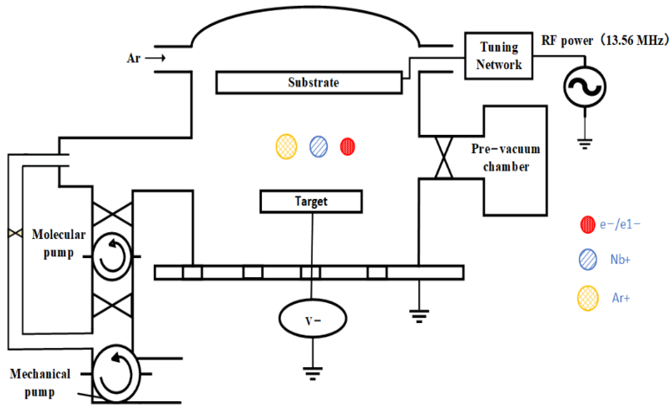
In traditional DC magnetron sputtering, the working gas particles (typically Ar) in the sputtering chamber are ionised near the target by colliding with electrons (e−) moving at high speeds under the influence of electromagnetic fields. The generated Ar+ ions bombard the target surface under the electric field to complete the sputtering process. As shown in Figure 1, compared with the traditional DC magnetron sputtering, an RF power source was added to the substrate, which supplied a frequency of 13.56 MHz. Because electrons move much faster than Ar+ ions, the RF power supply produced a negative bias, which promoted the entire sputtering process by guiding Ar+ and Nb+ ions in the sputtering chamber to bombard the substrate surface and improving the kinetic energy of Nb atoms, which both affected the deposition rate.
2.2. Experimental Procedure
Thin Nb films were deposited on silicon substrates (with ∼150 nm oxidation layers) using a two-chamber (load–lock chamber and process chamber) DC magnetron sputtering system (Kurt J. Lesker CSM18, Jefferson Hills, PA, USA).
The effects of the RF power on the properties of the Nb film were investigated using the control variable method. Therefore, the conventional process parameters remained unchanged during the deposition process. The substrate was 13 cm away from the Nb target, which was 99.95% pure. The DC sputtering power was set to 500 W and the sputtering pressure was maintained at 5 mTorr to control the free path between the sputtered particles, on the premise that the sputtering cavity could be turned on. The deposition time was set to 450 s to direct the film thickness. In addition, the substrate and target were equipped with cooling water devices, and the temperature was maintained at approximately 20 °C. Before transferring the substrate, the load–lock chamber was vacuumed with a mechanical pump and a molecular pump for approximately 2–3 h. Because the impurities on the substrate surface were not ideal, the RF pre-cleaning process was initiated when the pressure in the vacuum chamber reached 3 × 10⁻⁸ Torr by pumping in argon gas at 100 W for 300 s until the pressure reached 10 mTorr. During this process, the RF bias was approximately −287 V. Before the sputter deposition process, another 300 s of pumping was conducted to restore the vacuum degree of the process chamber to 3 × 10⁻⁸ Torr.
Under the above sputtering environment and process conditions, 0 W, 20 W, 40 W, and 60 W of RF power was provided to prepare four sets of samples. During the characterisation stage, the hardness, elastic moduli, and internal structures of the Nb film samples were tested. The crystal structure of the films was measured at room temperature (300 K) by X-ray diffraction (XRD, PANalytical X’pert PRO MRD, Malvern Panalytical, The Netherlands) with Cu-Kα radiation (λ = 0.15419 nm). The stress of the Nb film samples was measured and calculated using a multi-beam optical scanning curvature measurement system (kSA MOS Ultra Scan, k-Space ASSOCIATES, INC., Dexter, MI, USA). The indentation hardness and elastic moduli of the samples were measured via indentation tests using a Berkovich diamond tip with a nominal radius of curvature of 100 nm.
3. Results
3.1. RF Bias
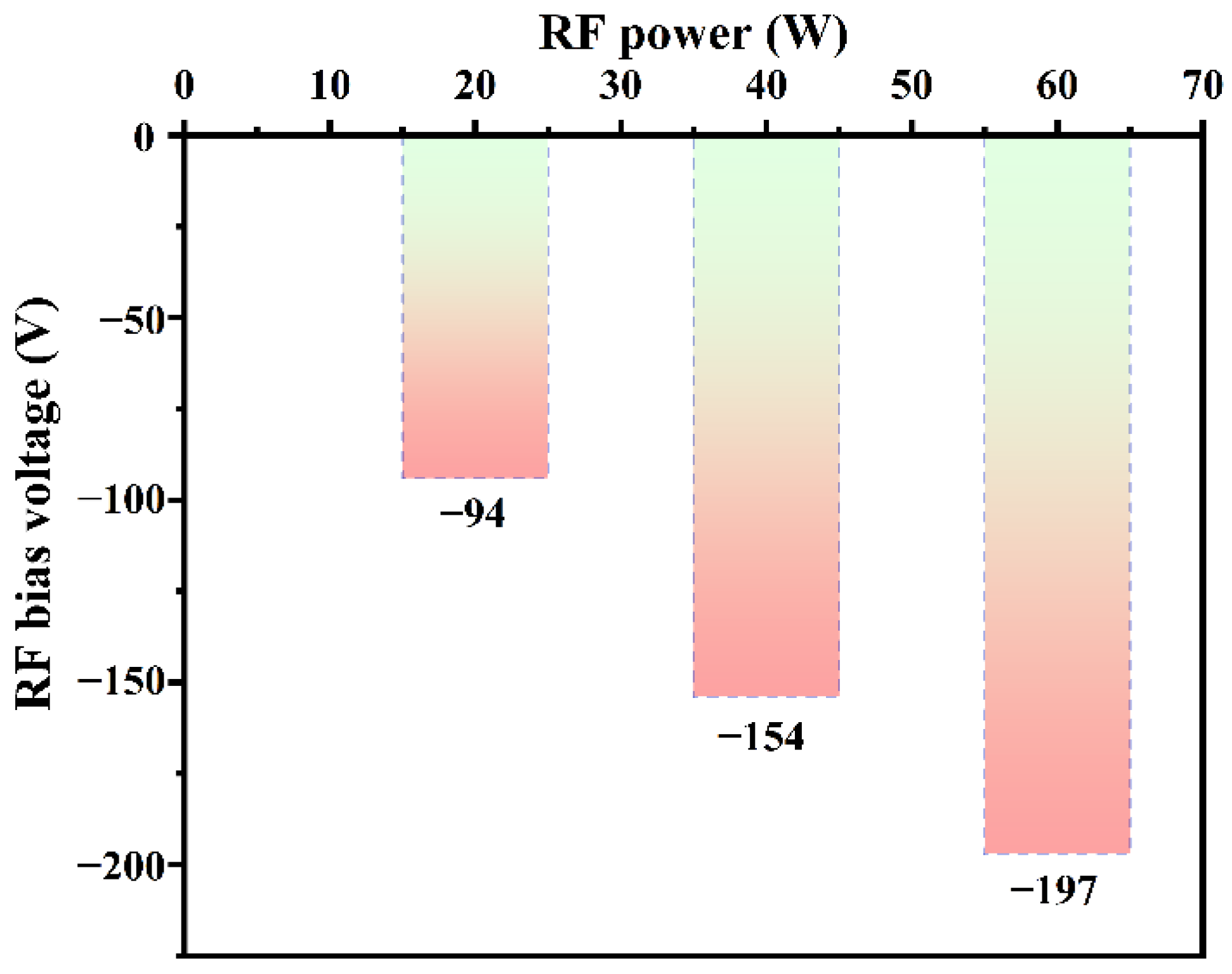
In this experiment, the amplitude of the RF bias was controlled by adjusting the RF power. As shown in Figure 2, no RF bias was produced at 0 W, while under RF powers of 20 W, 40 W, and 60 W, RF biases of −94 V, −154 V, and −197 V were produced, respectively. The substrate was used both as an anode and cathode for receiving ions, driven by an RF power supply [20]. Because electrons move much faster than ions, the substrate will accept a large number of electrons and become negatively charged during the positive half cycle of the power signal.
During the negative half cycle that follows, a small number of ions is received that move more slowly, neutralising the negative charge in the process. After a few cycles, the generated plasma exhibits a stable negative potential.
3.2. Film Stress
The thicknesses of the Nb films were 308.8 nm, 298.8 nm, 322.4 nm, and 319.1 nm for the films prepared at RF bias powers of 0 W, 20 W, 40 W, and 60 W, respectively. The stress of the Nb film was measured and calculated using a multi-beam optical scanning curvature measurement system (kSA MOS Ultra Scan, k-Space ASSOCIATES, INC., MI, USA). A negative value indicates that the stress of the Nb film is compressive, and a positive value indicates the occurrence of tensile stress. The minimum, maximum, average, and standard deviation of the Nb film stresses under different RF powers are shown in Figure 3. Figure 4 illustrates the direct variation trend of the stress with the RF power. Under zero RF bias, the compressive stress of the Nb film was −130.44 MPa. When the RF power was 20 W, the compressive stress of the Nb film increased rapidly to −691.79 MPa. Notably, when the RF powers were 40 W and 60 W, the compressive stresses of the Nb film were similar, namely −888.15 MPa and −883.72 MPa, respectively.
Although the film lattice remained undamaged under increased compressive stress, the excessive internal stress caused the film to fall off and curl, among other adverse effects. The generation mechanism of membrane compressive stress is complex. The deposition method and environmental conditions determine the stress state of the film. Under different deposition principles and environments, the film structure undergoes various changes. In the case of magnetron sputtering, there are three main factors affecting the structure of the resulting film: (1) the atomic shot peening effect during the sputtering process; (2) the variation of the lattice parameter with crystallite size and atomic rearrangement within the film; and (3) the grain boundaries, impurities, and defects in the films [21,22]. The change in the internal stress in the Nb film can be expressed by Equation (1):
where is the residual stress of the film, is the internal stress, and is the thermal stress.
The RF power, which guides the continuous bombardment of Ar+ ions on the surface of the Nb film during the sputtering process, can result in the pinning of some Ar+ ions on the surface of the Nb film and the subsequent formation of impurities. In addition, Ar+ ion bombardment induces complex physical movements within the Nb film, such as cascade collisions, which cause the inner grains to squeeze each other and deform and increase the internal stress.
3.3. Crystal Structure
We employed standard procedures for the structural characterisation of the thin Nb films that have been reported elsewhere [23,24]. The crystal structures of the films were measured via XRD in the 2θ scanning range of 10–90°. The X-ray incidence angle was set to 1° to the film surface to pass through Si substrate’s signal on the scanning results. Finally, Gaussian fitting was used on the peaks to remove some irregular points and improve the interpretability. Figure 5 shows the XRD patterns of the Nb film deposited at various RF powers. When the X-rays were at the incident angle (2θ), diffraction peaks appeared at 38.5°, 55.6°, 69.7°, and 82.5°, corresponding to the (110), (200), (211) and (220) crystal planes of the Nb film grains, respectively. The Nb film exhibited a body-centred cubic (bcc) structure [25], and the (110) planes with the lowest surface energy were closely packed.
The changes in the diffraction peak intensities can be seen in Figure 5, which reflect the crystallinity of the film. The Nb film presented a polycrystalline structure, and the XRD results showed that the diffraction peaks on the (110) and (211) crystal planes were the most obvious. The effect of RF bias on the crystal distribution in niobium films can be judged by the intensity ratio of I(110)/I(211), where I(110) and I(211) represent different crystal plane diffraction peak intensities, respectively.
When the RF power was 0 W, the ratio of I(110)/I(211) was 1.09, which indicates that the diffraction peak intensities on the (110) and (211) planes were almost similar. When the RF power increased to 20 W, the ratio of I(110)/I(211) increased to 1.34. When the RF power further increased to 40 W and 60 W, I(110)/I(211) decreased to 0.99 and 0.59 respectively.
The change in the crystal distribution in the film was mainly due to the change in the mobility of the deposited particles, which was a non-equilibrium process governed by the competition between kinetics and thermodynamics [24,25,26]. Therefore, the change in the preferred orientation of the crystal plane in the Nb film under different RF powers was due to the atoms’ migration on the film surface.
The grain size is an important index used to evaluate the growth of thin films. Regarding the mechanical properties, a refined grain size implies the improved strength and fatigue resistance of the Nb material. As a polycrystalline film, the grain size of the Nb film is affected by various parameters. Figure 6a shows the full-width at half-maximum (FWHM) data of the diffraction peaks of the (110) crystal plane, which were 0.536, 0.552, 0.575, and 0.662 when the RF powers were 0 W, 20 W, 40 W, and 60 W, respectively. It is shown that the FWHM increased when the RF power was raised.
The average grain size (g) can be evaluated using Scherrer’s formula [27,28]:
where (0.15419 nm for Cu–Kα radiation) is the wavelength of the X-ray radiation, FWHM is the full-width at half-maximum of the peaks, and is the angle between the incident X-rays. The grain size of the (110) crystal plane was calculated using Equation (2), and its changing trend is shown in Figure 6b. It was shown that the grain size decreased with the raised RF power, which were 16 nm, 15.5 nm, 14.9 nm and 12.8 nm when the RF powers were 0 W, 20 W, 40 W and 60 W respectively.
Under the influence of the RF bias, the positive ions bombarding the surface of the Nb film was a process that lasted for the entire sputtering stage. This had the following two effects: (1) the ion bombardment-induced defects and higher re-nucleation rates caused the grain size to decrease; (2) the positive ion bombardment improved the mobility of the Nb atoms and clusters [29].
As shown in Figure 7a, under a constant X-ray incident angle, as the RF power increased, the occurrence angles of all diffraction peaks on the same crystal plane of the Nb film gradually decreased, which indicated lattice expansion. To further confirm the correlation between the lattice expansion of the Nb film and the RF power, we calculated the changes in the lattice parameters (a) on the crystal plane of the Nb film (110) using Equation (3) (Bragg’s law) and Equation (4):
where is the interplanar spacing, is the wavelength of the X-ray radiation used, is the angle between the incident X-ray and the crystal plane, and , , and are the crystal plane indices.
The lattice parameter variation of the Nb thin film with the RF power is illustrated in Figure 7b. The lattice parameter varied from 3.297 Å to 3.315 Å as the RF power varied from 0 W to 60 W. Generally, the lattice parameters of the Nb films prepared by introducing RF power were relatively larger than those of the bulk Nb by 3.30 Å. This variation in the lattice parameter is expected to result in the generation of the residual compressive stress, which is consistent with the stress measurement results in Section 3.2.
3.4. Hardness and Elastic Modulus
The hardness and the elastic moduli of the Nb films were tested using an Anton Parr UNHT indentation instrument. For the tests, the maximum load was 0.3 mN. The load function was 15 s in the loading stage, followed by a 5 s pause and 15 s in the unloading stage. Each sample was tested five times. The Poisson’s ratio (nu) was set to 0.30 in the data analysis process. Figure 8 shows the load-displacement nano scaling curve of the Nb films prepared under different RF powers. The hardness and elastic modulus were extracted using the Oliver and Pharr methods [30], and the average values and standard deviations of the data are given in Table 1. The average hardness of the Nb film was between 4.17 GPa and 5.34 GPa and increased along with the RF power. This behaviour was attributed to the following two reasons: (1) the internal grain size of the Nb film decreased along with the increasing RF power; and (2) under the guidance of the RF power, the bombardment of Ar+ ions on the surface of the Nb film penetrated the interior and increased the film’s density [31,32]. It can be therefore concluded that Nb films with higher hardness values can be obtained under higher RF bias voltages.
Table 1 shows that the elastic moduli of the Nb films were all around 140.70 GPa. Under the same external force, the lower the elastic modulus of the film, the more susceptible it was to deformation (but the better its flexibility). On the contrary, the higher the elastic modulus, the more difficult it was for the film to deform, but its brittleness was more robust. The results show that the elastic moduli of the Nb films were not affected by adjusting the RF bias voltage.
4. Conclusions
In this study, the stresses, internal structures, and hardnesses of Nb films that were DC-sputtered under different RF powers were analysed. The results show that RF bias effectively changed the growth pattern and grain size of the internal structure of the film. The stress of the Nb film was compressive, and the hardness of the film increased from 4.17 GPa to 5.34 GPa with an elevated RF power from 0 W to 60 W. This study aimed to enhance the mechanical properties of Nb films deposited by RF-biased sputtering. The results show that the RF power can effectively improve the mechanical properties and internal structure of deposited Nb films, which provides wider potential for Nb films as protective coatings for medical–biological implant bodies. Although this research was carried out on Si substrates to facilitate the study of film stress, we believe that the evolution trends of our results will also apply to other metal substrates, because the film mechanical properties are intrinsic.
Author Contributions
Conceptualization, Y.Z. and Z.N.; methodology, Y.Z. and Z.N.; validation and testing, Z.N., X.T., W.L. and H.G.; formal analysis, Y.Z. and Z.N.; investigation, Y.Z.; resources, Y.Z. and Y.Y.; data curation, Z.N.; writing logic guidance Y.Z. and Y.Y.; writing—original draft preparation, Z.N.; writing—review and editing, Y.Z.; visualization, Z.N.; supervision, Y.Z.; project administration, Y.Z.; funding acquisition, Y.Z. All authors have read and agreed to the published version of the manuscript.
Funding
This research was supported in part by the National Natural Science Foundation of China (Grant No. 61971471), and in part by the Strategic Priority Research Program of Chinese Academy of Sciences under Grant XDC07010100.
Institutional Review Board Statement
Not applicable.
Informed Consent Statement
Not applicable.
Data Availability Statement
The data are contained within the article.
Acknowledgments
The authors thank Wenhui Cao, Huang Lu, Xu Li, and Jian Chen for their helpful discussion.
Conflicts of Interest
The authors declare no conflict of interest.
References
- Godmann, S.B.; Davidson, J.A.; Fornasier, V.L.; Mishra, A.K. Histological response to cylinders of a low modulus Titanium alloy (Ti-13Nb-13Zr) and a wear resistant Zirconium alloy (Zr-2.5Nb) implanted in the rabbit tibia. J. Appl. Biomater. 1993, 4, 331–339. [Google Scholar] [CrossRef]
- Matsuno, H.; Yokoyama, A.; Watari, F.; Uo, M.; Kawasaki, T. Biocompatibility and osteogenesis of refractoy metal implants, titanium, hafnium, niobium, tantalum and rhenium. Biomaterials 2001, 22, 1253–1262. [Google Scholar] [CrossRef]
- Eisenbarth, E.; Velten, D.; Müller, M.; Thull, R.; Brene, J. Biocompatibility of β-stabilizing elements of titanium alloys. Biomaterials 2004, 25, 5705–5713. [Google Scholar] [CrossRef]
- Olivares-Navarrete, R.; Olaya, J.J.; Ramírez, C.; Rodil, S.E. Biocompatibility of niobium coatings. Coatings 2011, 1, 72–87. [Google Scholar] [CrossRef]
- Iosad, N.N.; Klapwijk, T.M.; Polyakov, S.N.; Roddatis, V.V.; Kov’ev, E.K.; Dmitriev, P.N. Properties of DC magnetron sputtered Nb and NbN films for different source conditions. IEEE Trans. Appl. Supercond. 1999, 9, 1720–1723. [Google Scholar] [CrossRef]
- Wu, C.T. Intrinsic stress of magnetron-sputtered niobium films. Thin Solid Films 1979, 64, 103–110. [Google Scholar] [CrossRef]
- Gao, H.; Wang, S.; Xu, D.; Wang, X.; Zhong, Q.; Zhong, Y.; Li, J.; Cao, W. Study of DC Magnetron Sputtered Nb Films. Crystals 2022, 12, 31. [Google Scholar] [CrossRef]
- Dobrovolskiy, O.V.; Huth, M. Crossover from dirty to clean superconducting limit in dc magnetron-sputtered thin Nb films. Thin Solid Films 2012, 520, 5985–5990. [Google Scholar] [CrossRef]
- De Freitas, T.C.; Gonzalez, J.L.; Nascimento, V.P.; Passamani, E.C. The role of the substrate temperature on superconducting properties of sputtered Nb films. Thin Solid Films 2016, 611, 33–38. [Google Scholar] [CrossRef]
- Li, X.; Cao, W.H.; Tao, X.F.; Ren, L.L.; Zhou, L.Q.; Xu, G.F. Structural and nanomechanical characterization of niobium films deposited by DC magnetron sputtering. Appl. Phys. A 2016, 122, 505. [Google Scholar] [CrossRef]
- Valente-Feliciano, A.M. Nb films: Substrates, nucleation & crystal growth. In Proceedings of the 15th International Conference on RF Superconductivity, Chicago, IL, USA, 25–29 July 2011; pp. 332–342. [Google Scholar]
- Okolo, B.; Lamparter, P.; Welzel, U.; Mittemeijer, E.J. Stress, texture, and microstructure in niobium thin films sputter deposited onto amorphous substrates. J. Appl. Phys. 2004, 95, 466–476. [Google Scholar] [CrossRef]
- Zhang, K.; Wen, M.; Meng, Q.N.; Hu, C.Q.; Li, X.; Liu, C.; Zheng, W.T. Effects of substrate bias voltage on the microstructure, mechanical properties and tribological behavior of reactive sputtered niobium carbide films. Surf. Coat. Technol. 2012, 212, 185–191. [Google Scholar] [CrossRef]
- Sekhar, M.C.; Kondaiah, P.; Chandra, S.J.; Rao, G.M.; Uthanna, S. Effect of substrate bias voltage on the structure, electric and dielectric properties of TiO2 thin films by DC magnetron sputtering. Appl. Surf. Sci. 2011, 258, 1789–1796. [Google Scholar] [CrossRef]
- Khamseh, S.; Alibakhshi, E.; Ramezanzadeh, B.; Sari, M.G. A tailored pulsed substrate bias voltage deposited (aC: Nb) thin-film coating on GTD-450 stainless steel: Enhancing mechanical and corrosion protection characteristics. Chem. Eng. J. 2021, 404, 126490. [Google Scholar] [CrossRef]
- Imamura, T.; Hasuo, S. Effects of intrinsic stress on sub-micrometer Nb/AlO/sub x//Nb Josephson junctions. IEEE Trans. Magn. 1989, 25, 1119–1122. [Google Scholar] [CrossRef]
- Amos, R.S.; Breyer, P.E.; Huang, H.H.; Lichtenberger, A.W. Stress and source conditions of DC magnetron sputtered Nb films. IEEE Trans. Appl. Supercond. 1995, 5, 2326–2329. [Google Scholar] [CrossRef]
- Ding, J.C.; Mei, H.; Jeong, S.; Zheng, J.; Wang, Q.M.; Kim, K.H. Effect of bias voltage on the microstructure and properties of Nb-DLC films prepared by a hybrid sputtering system. J. Alloys Compd. 2021, 861, 158505. [Google Scholar] [CrossRef]
- Huang, K.; Li, L.; Wang, L.; Li, G.; Xu, Y. Effect of DC bias and RF self-bias on the structure and properties of chromium oxide coatings prepared by vacuum cathodic arc deposition. Vacuum 2019, 164, 325–331. [Google Scholar] [CrossRef]
- Ou, J.; Men, Z. Formation of the radio frequency sheath of plasma with Cairns–Tsallis electron velocity distribution. Phys. Plasmas 2020, 27, 083517. [Google Scholar] [CrossRef]
- Doerner, M.; Nix, W. Stresses and deformation processes in thin films on substrates. Crit. Rev. Solid State Mater. Sci. 1988, 14, 225–268. [Google Scholar] [CrossRef]
- Windischmann, H. Intrinsic stress in sputter-deposited thin films. Crit. Rev. Solid State Mater. Sci. 1992, 17, 547–596. [Google Scholar] [CrossRef]
- Battu, A.K.; Makeswaran, N.; Ramana, C.V. Fabrication, characterization and optimization of high conductivity and high quality nanocrystalline molybdenum thin films. J. Mater. Sci. Technol. 2019, 35, 2734–2741. [Google Scholar] [CrossRef]
- Battu, A.K.; Zade, V.B.; Deemer, E.; Ramana, C.V. Microstructure-Mechanical Property Correlation in Size Controlled Nanocrystalline Molybdenum Films. Adv. Eng. Mater. 2018, 20, 1800496. [Google Scholar] [CrossRef]
- Xiang, P.; Liu, J.S.; Li, M.Y.; Yang, H.F.; Liu, Z.T.; Fan, C.C.; Shen, D.W.; Wang, Z.; Liu, Z. In Situ Electronic Structure Study of Epitaxial Niobium Thin Films by Angle-Resolved Photoemission Spectroscopy. Chin. Phys. Lett. 2017, 34, 077402. [Google Scholar] [CrossRef]
- Nivedita, L.R.; Haubert, A.; Battu, A.K. Correlation between crystal structure, surface/interface microstructure, and electrical properties of nanocrystalline niobium thin films. Nanomaterials 2020, 10, 1287. [Google Scholar] [CrossRef]
- Hussein, E.T.A.; Yousif, B.A. Effect of silver nanoparticle on structural and some (optical, electrical) properties of poly (vinyl chloride) films AIP Conference Proceedings. AIP Publ. LLC 2020, 2213, 020199. [Google Scholar] [CrossRef]
- Holzwarth, U.; Gibson, N. The Scherrer equation versus the ‘Debye-Scherrer equation’. Nat. Nanotechnol. 2011, 6, 534. [Google Scholar] [CrossRef]
- Bunshah, R.F.; Weissmantel, C. Handbook of Hard Coatings; Noyes Publications: Park Ridge, NJ, USA, 2001; Volume 3, pp. 77–107. [Google Scholar]
- Oliver, W.C.; Pharr, G.M. An improved technique for determining hardness and elastic modulus using load and displacement sensing indentation experiments. J. Mater. Res. 1992, 7, 1564–1583. [Google Scholar] [CrossRef]
- O’Brien, B. Niobium Biomaterials; Springer: Berlin/Heidelberg, Germany, 2015. [Google Scholar] [CrossRef]
- Caicedo, J.C.; Gonzalez, R.; Caicedo, H.H.; Gholipourmalekabadi, M.; Amaya, C. Mechanical and tribological properties of V–C–N coatings as a function of applied bias voltage. J. Superhard Mater. 2016, 38, 337–350. [Google Scholar] [CrossRef]
Figure 1.
Processing chamber scheme.

Figure 2.
Correlation between RF bias and RF power.

Figure 3.
Stress mappings for samples deposited under various RF bias powers: (a) 0 W, (b) 20 W, (c) 40 W, and (d) 60 W.
Figure 3.
Stress mappings for samples deposited under various RF bias powers: (a) 0 W, (b) 20 W, (c) 40 W, and (d) 60 W.


Figure 4.
Film stress of the samples deposited under various RF bias powers.

Figure 5.
XRD patterns of the Nb films deposited under various RF bias powers.

Figure 6.
(a) FWHMs of the (110) crystal plane diffraction peak and (b) grain sizes of the Nb films deposited under different RF bias powers.
Figure 6.
(a) FWHMs of the (110) crystal plane diffraction peak and (b) grain sizes of the Nb films deposited under different RF bias powers.

Figure 7.
(a) Diffraction angle offset and (b) lattice parameters of the Nb films deposited under RF bias powers.
Figure 7.
(a) Diffraction angle offset and (b) lattice parameters of the Nb films deposited under RF bias powers.

Figure 8.
Load-displacement nanoindentation curves of the films deposited under different RF bias powers.
Figure 8.
Load-displacement nanoindentation curves of the films deposited under different RF bias powers.


Table 1.
Hardness and elastic moduli of the Nb films deposited under different RF bias powers, calculated based on the load-displacement curves.
Table 1.
Hardness and elastic moduli of the Nb films deposited under different RF bias powers, calculated based on the load-displacement curves.
| RF Bias Power (W) | Hardness (GPa) | Elastic Modulus (GPa) |
|---|---|---|
| 0 | 4.17 ± 0.45 | 143.19 ± 18.49 |
| 20 | 4.42 ± 0.65 | 138.82 ± 21.21 |
| 40 | 5.16 ± 0.59 | 140.70 ± 5.08 |
| 60 | 5.34 ± 0.58 | 140.72 ± 13.76 |
Publisher’s Note: MDPI stays neutral with regard to jurisdictional claims in published maps and institutional affiliations. |
© 2022 by the authors. Licensee MDPI, Basel, Switzerland. This article is an open access article distributed under the terms and conditions of the Creative Commons Attribution (CC BY) license (https://creativecommons.org/licenses/by/4.0/).
Share and Cite
MDPI and ACS Style
Ni, Z.; Zhong, Y.; Tao, X.; Li, W.; Gao, H.; Yao, Y. Effects of Radio Frequency Bias on the Structure Parameters and Mechanical Properties of Magnetron-Sputtered Nb Films. Crystals 2022, 12, 256. https://doi.org/10.3390/cryst12020256
AMA Style
Ni Z, Zhong Y, Tao X, Li W, Gao H, Yao Y. Effects of Radio Frequency Bias on the Structure Parameters and Mechanical Properties of Magnetron-Sputtered Nb Films. Crystals. 2022; 12(2):256. https://doi.org/10.3390/cryst12020256
Chicago/Turabian StyleNi, Zegang, Yuan Zhong, Xingfu Tao, Wei Li, Huifang Gao, and Yan Yao. 2022. "Effects of Radio Frequency Bias on the Structure Parameters and Mechanical Properties of Magnetron-Sputtered Nb Films" Crystals 12, no. 2: 256. https://doi.org/10.3390/cryst12020256
Note that from the first issue of 2016, this journal uses article numbers instead of page numbers. See further details here.