Article

Charge State Effects in Swift-Heavy-Ion-Irradiated Nanomaterials

1
Ruđer Bošković Institute, Bijenička 54, 10000 Zagreb, Croatia
2
National Institute of Materials Physics, Atomistilor 405A, 077125 Magurele, Romania
3
Faculty of Physics, University of Bucharest, Atomistilor 405, 077125 Magurele, Romania
*
Author to whom correspondence should be addressed.
Crystals 2022, 12(6), 865; https://doi.org/10.3390/cryst12060865
Submission received: 26 May 2022 / Revised: 13 June 2022 / Accepted: 16 June 2022 / Published: 19 June 2022
(This article belongs to the Special Issue 2D Crystalline Nanomaterials)

Abstract

:
The aim of this experimental work was to investigate the influence of the ion beam charge state on damage production in nanomaterials. To achieve this, we employed Raman spectroscopy, atomic force microscopy, and transmission electron microscopy to investigate nanomaterials irradiated by a 23 MeV I beam. We found a significant influence of the ion charge state on damage production in monolayer graphene, but found no evidence of this effect in bilayer and trilayer graphene, nor in graphite. Furthermore, we found no evidence of this effect in CaF2 and SiO2 nanocrystals irradiated with the same ion beam.

1. Introduction

Heavy ion irradiation is a versatile tool for materials nanostructuring, particularly for 2D materials and surfaces [1,2]. Usually, ion beam irradiation parameters (such as ion type, energy, fluence, and angle of irradiation) can be controlled to a great degree, and consequently, the effects of irradiation can be precisely tuned [3,4,5]. High-energy heavy ion irradiation offers some additional benefits, such as an extended ion range in materials and cylindrical-shaped permanent damage along the ion path, called an ion track. Among a plethora of other applications, high-energy heavy ion irradiation (often called swift heavy ion (SHI) irradiation) has found use in the production of nanomembranes, as ion tracks in thin polymer films can be easily etched away. Membranes produced in this way have narrow pore size distribution, while porosity can be easily tuned by the applied ion fluence. Furthermore, by placing graphene on the polymer substrate, this approach offers a facile route for the production of graphene nanomembranes with exceptionally small nanopores [6].
Another advantage of SHI irradiation (related to the straight path of the SHI through the material) is its exceptional usefulness in 2D materials and surface nanostructuring when irradiation is performed under the grazing angle of incidence. This approach enables exciting possibilities of producing unique structures on material surfaces, such as chains of nanodots [7], perforated graphene [8] and nanoscale ripples [9]. However, understanding and describing mechanisms leading to the formation of such nanostructures remain challenging. For example, the deposition and retention of SHI energy in thin films are difficult to model, but recently, some progress has been made [10,11,12].
In the present work, we investigate the effects of the SHI charge state on the response of the nanomaterials to the SHI irradiation. Depending on its velocity, SHI acquires an equilibrated charge state during passage through the material due to numerous collisions with electrons. Many experimental and theoretical works studied this effect, because deceleration of the SHI due to inelastic collisions with electrons (i.e., electronic stopping) is dependent on the SHI charge state, and thus SHI velocity [13]. This is important because materials’ modification under SHI irradiation (i.e., ion track formation) depends on the density of SHI-deposited energy. In the bulk, this is equal to the electronic stopping of SHI, but on the surface or within 2D material, this might not be the case. The reason for this is that in nanomaterials, not all of the deposited energy is retained within the SHI impact site [10,11,12]. Furthermore, SHI delivered by the ion accelerator often has a charge state lower than the equilibrated one, and such SHI deposits less energy into the nanomaterial than the fully equilibrated one. Since the amount of deposited energy in the primary stage of the ion track formation is a critical parameter that profoundly affects later stages of ion track formation (irrespectively of the damage formation mechanisms), concerns have been voiced over the necessity of using the so-called stripper foil in SHI irradiation experiments on nanomaterials [14,15,16]. Additionally, well-known recrystallisation of the ion tracks in the bulk can be suppressed in the near-surface regions [17]. Thus, in the case of thin films and nanomaterials, surface proximity can make nanomaterials prone to radiation damage if recrystallisation, as a way to heal material after the ion impact, is inactive. To correctly evaluate the radiation hardness of nanomaterials, it might be necessary to exclude possible charge state effects (that can occur in the same near-surface region) by using equilibrated ion beams.
Thus, the purpose of this work was to investigate the influence of the ion charge state in experiments where SHI beam is used for the nanostructuring of nanomaterials, and to establish conditions when the use of stripper foils is mandatory.

2. Experimental Details

Samples of monolayer, bilayer and trilayer graphene were purchased from Graphenea (San Sebastian, Spain). Graphene samples were grown by the chemical vapor deposition (CVD) method, and later transferred onto 90 nm thick amorphous SiO2 film on top of a Si wafer. High-quality, highly oriented pyrolytic graphite (ZYA grade HOPG) samples were purchased from 2SPI (West Chester, PA, USA). The CaF2 samples were purchased from Korth (Altenholz, Germany) and quartz SiO2 samples were purchased from Crystec (Berlin, Germany). For the TEM measurements, CaF2 and SiO2 samples were crushed in the mortar and the obtained nanocrystal grains were deposited on the TEM grids before irradiation. Deposition was achieved by dispersing nanocrystals in ethanol and dripping the solution on the TEM grid, followed by drying in ambient conditions [18].
All samples were irradiated using 6 MV EN Tandem Van de Graaff accelerator (HVEC, Burlington, MA, USA) at the Ruđer Bošković Institute in Zagreb. In the present study, a 23 MeV I6+ ion beam was used. The scanning ion beam irradiation was carried out at normal incidence and at room temperature at the ToF-ERDA beamline [18,19]. Applied fluences were within the range of 1011–5 × 10¹³ ions/cm2. The ion beam fluence was established by the ion current measurements in the Faraday cup both before and after the exposures. Longer exposures were occasionally interrupted for current monitoring. We estimate that the fluence measurements errors were less than 10%. Graphene and HOPG samples were exposed multiple times because the ion irradiation exposed areas were 3 × 2 mm2 in size, while the samples were 1 × 1 cm2 in size.
All samples were irradiated using either ion beam with Q = 6+ charge state or with fully equilibrated ion beam obtained after passing through 100 nm thin carbon foil (Micromatter, Surrey, Canada). Equilibration of the used ion beam results in an increase in the ion charge state from Q = 6+ to Q = 14+ (with the FWHM Q = 5 of the resulting charge state distribution) and, consequently, an increase in the electronic stopping power [20]. The change in the kinetic energy of the ion when passing through the thin carbon stripper foil is less than 700 keV, which decreases electronic stopping by only 2% [21]. The value of the nuclear stopping is less than 5% of the electronic stopping [21], and is not influenced by the charge state of the ion [22]. In Table 1, all ion irradiation parameters obtained by the SRIM 2013 [21] and CasP 5.2 [20] codes are given. The SRIM code is the most often used code for the calculation of ion stopping and range in materials, and is considered a standard for the parametrisation of ion track experiment results [4,5,9,12,15]. We used both codes because the SRIM code can calculate both nuclear and electronic stopping, but can only calculate electronic stopping for fully equilibrated ions. On the other hand, the CasP code can calculate the ion charge state-dependent electronic stopping power, but cannot calculate nuclear stopping [20]. The range of the ions is typically several micrometres, i.e., they completely pass through the studied nanomaterials, so the effects of the ion implantation are not relevant.
After the irradiation, graphene and graphite samples were investigated by Raman spectroscopy measurements within several hours. For this, Raman spectrometer Horiba Jobin Yvon T64000 located at the RBI was used. A 532 nm laser with a 50× long working distance objective and the power of a few mW was used for excitation. Additionally, monolayer graphene samples were investigated with atomic force microscope (AFM) N’Tegra Prima from NT-MDT. The AFM was operated in the tapping mode using NT-MDT cantilevers with resonance frequencies of approximately 130 kHz. Images were analysed using the Gwyddion code [23], and only the polynomial background was subtracted from the rows that were aligned to the same median level. No additional surface treatment (cleaning, annealing, etc.) was carried out during this investigation.
After the irradiation, CaF2 and SiO2 nanocrystals were studied with a JEM 2100 transmission electron microscope operated at 200 kV acceleration voltage and at room temperature. Procedures from ref. [18] were followed to avoid electron beam-induced defects in the studied samples.

3. Results and Discussion

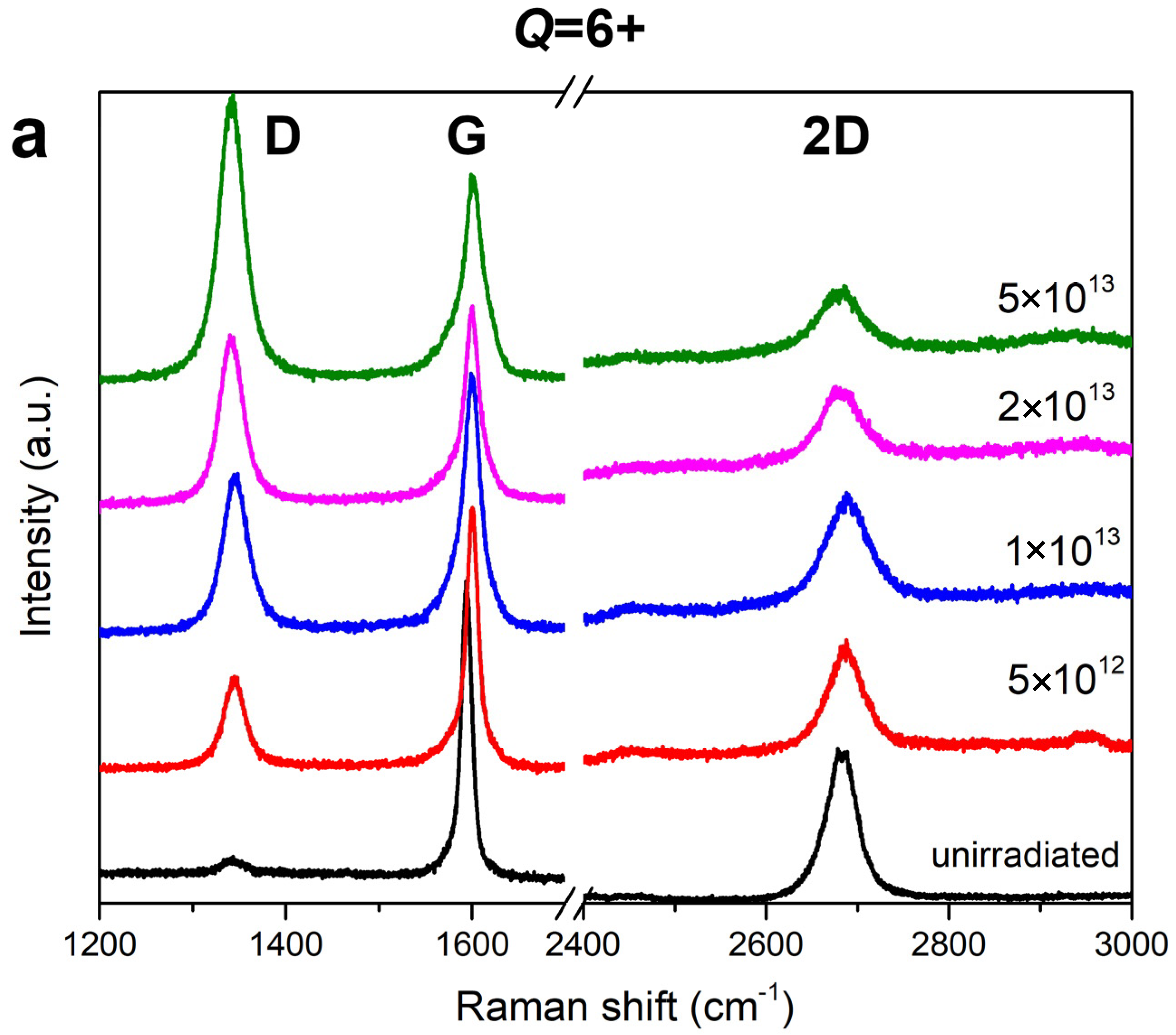
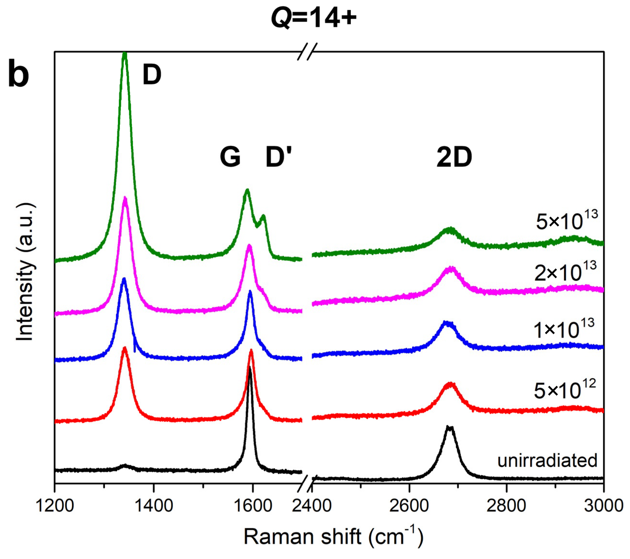
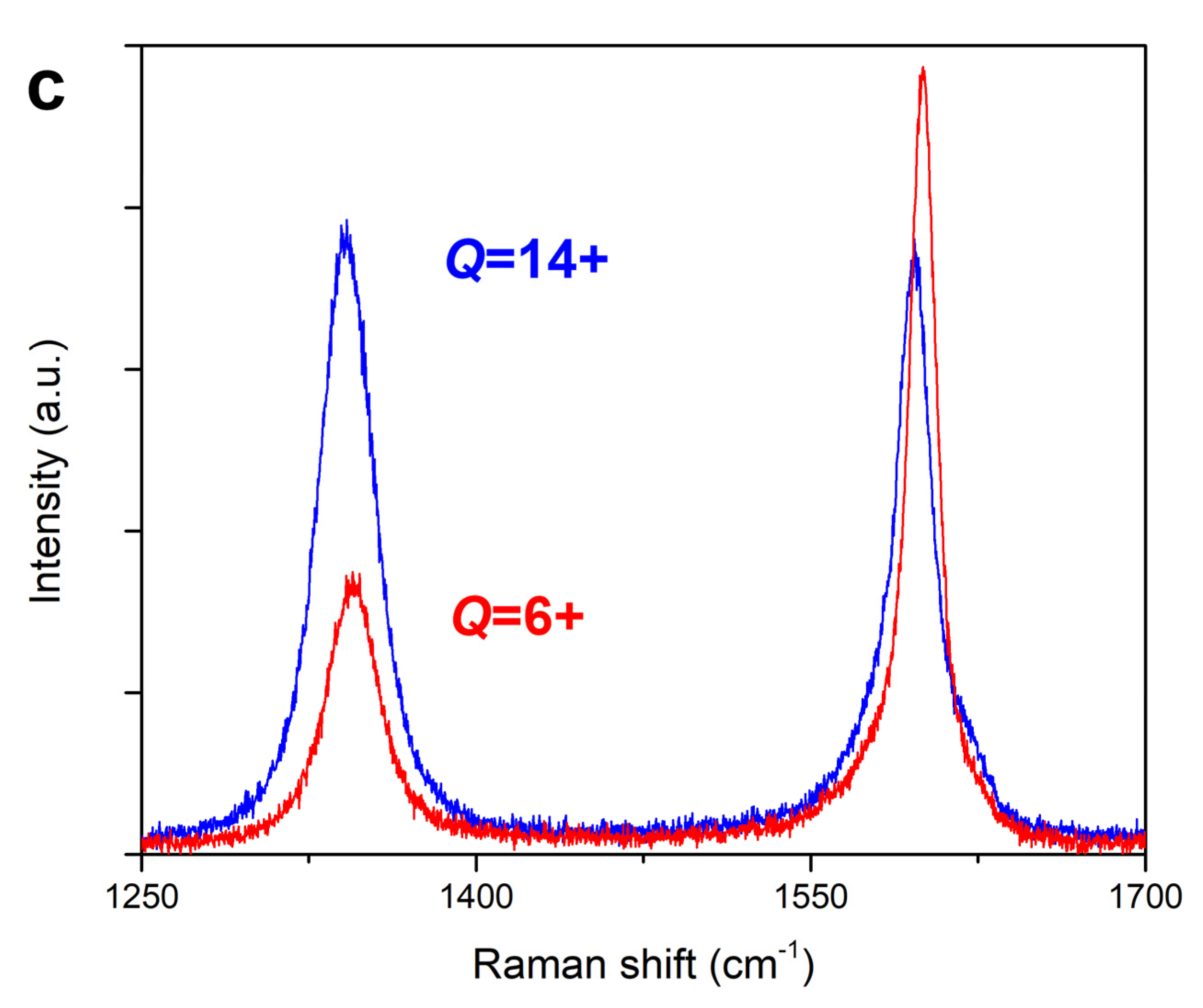
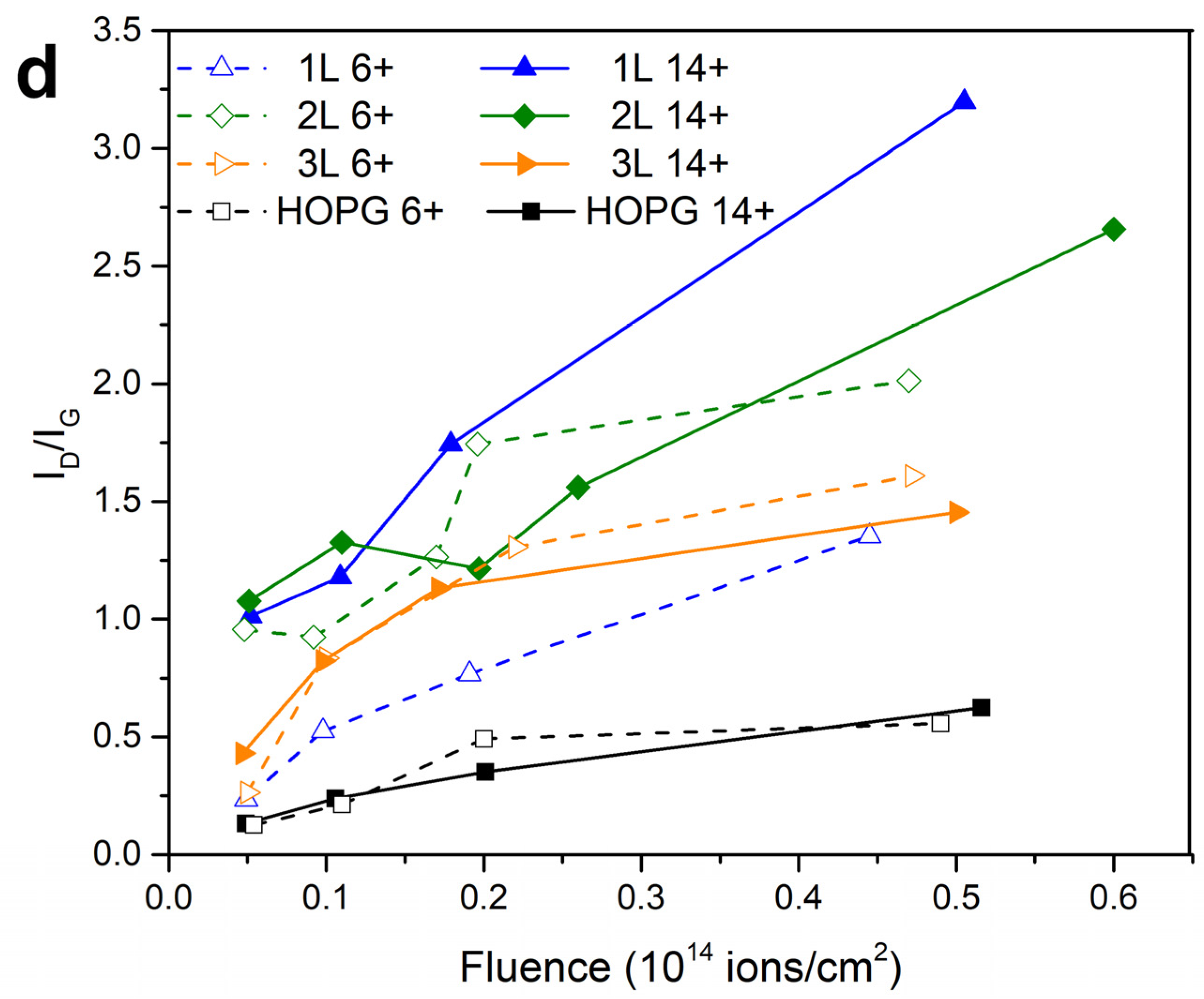
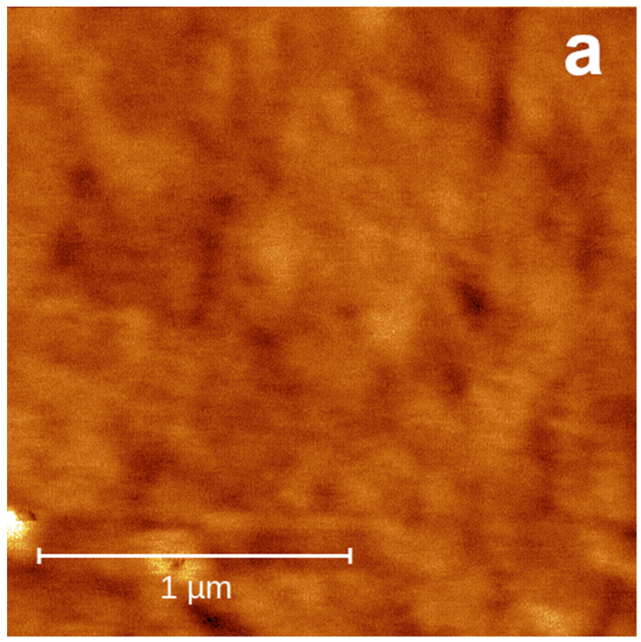
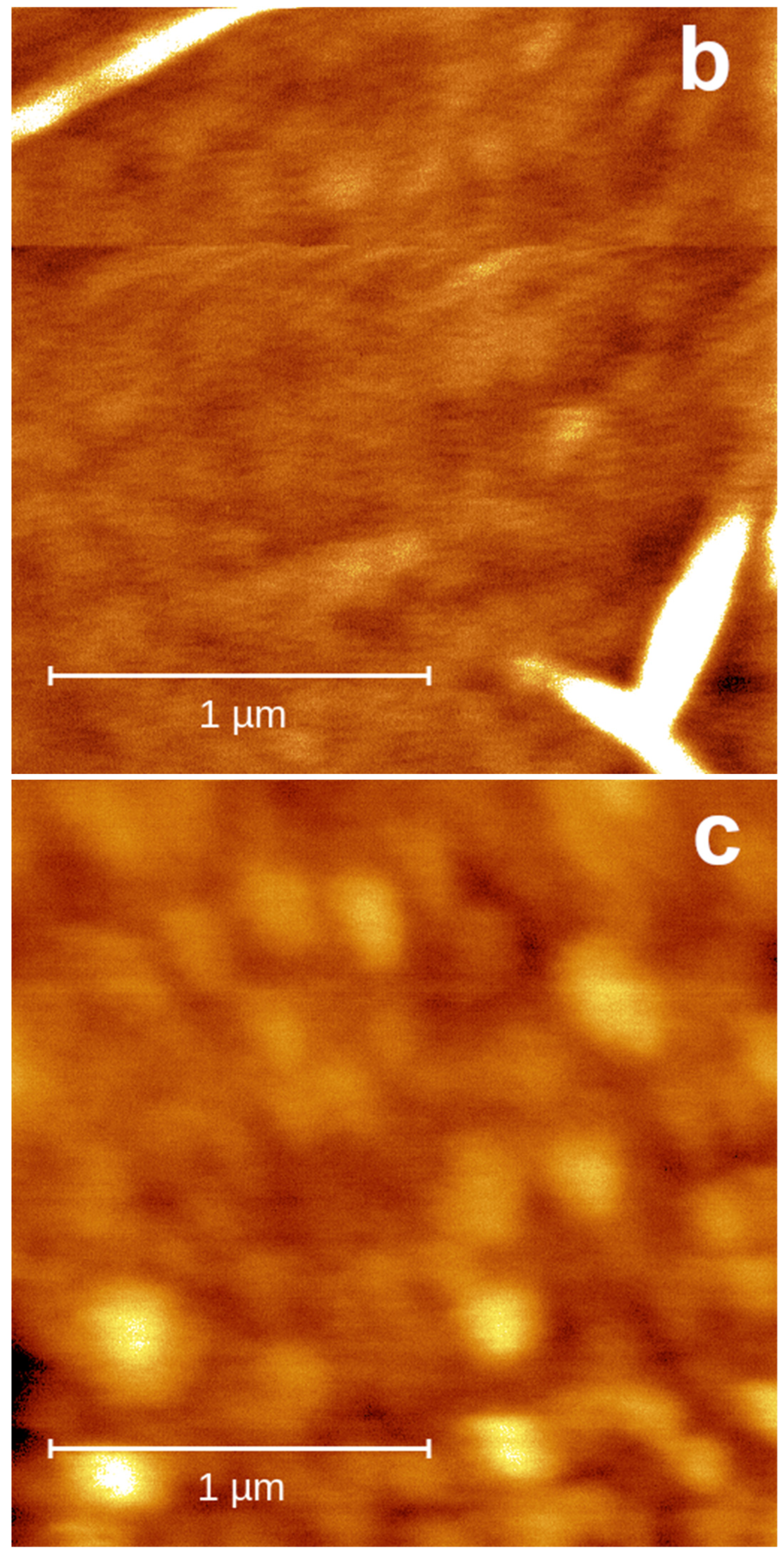
3.1. Graphene and Graphite

Raman spectra from the irradiated monolayer graphene samples are presented in Figure 1. The Raman spectrum from the unirradiated part of the sample shows good crystallinity with a rather low number of defects from CVD growth and transfer, as the defect-activated D peak at 1350 cm−1 is very small. Other peaks analysed here, namely, G mode at 1580 cm−1 and 2D mode at 2700 cm−1, are well visible, while another defect-activated peak from D’ mode at 1620 cm−1 is absent. As expected, damage in graphene accumulates by applying increasing SHI irradiation fluence. Raman spectra in Figure 1a show a steady increase in the D peak together with a decrease in the G peak when ion fluence is increased from 5 × 10¹² ions/cm2 to 5 × 10¹³ ions/cm2. We also observed the reduction in the 2D peak with increasing fluence. The spectra on Figure 1a were collected from a monolayer graphene sample irradiated with the 23 MeV iodine beam with the charge state of Q = 6+, i.e., as delivered from the Tandem accelerator. For comparison, in Figure 1b, we present Raman spectra collected from another monolayer graphene sample, irradiated with the same ion beam, but in this case, thin carbon foil was placed in front of the sample. As described previously, the foil increased the charge state of the ion beam up to the Q = 14+, while the kinetic energy of the ions was decreased by only ~700 keV. This small decrease in the kinetic energy resulted in negligible changes to the stopping powers, but the change in the ion charge state had a significant influence on the electronic stopping power, as shown in Table 1. Therefore, while the damage kinetics are similar both in Figure 1a and in Figure 1b, it is clear the same amount of damage is produced for much lower fluences in Figure 1b. For example, the shoulder on the G peak, i.e., the appearance of the D’ peak, is found already at a fluence of 2 × 10¹³ ions/cm2 in Figure 1b, while the D’ peak is never observed (even for the highest fluence of 5 × 10¹³ ions/cm2) in Figure 1a. This indicates that more damage has been inflicted on the graphene by 2 × 10¹³ ions/cm2 fluence of the Q = 14+ charge state ion beam than with 5 × 10¹³ ions/cm2 fluence of the Q = 6+ charge state ion beam. The same conclusion can be achieved by comparison of the spectra in Figure 1a,b for a given ion fluence. As an example, Raman spectra for both charge states and for common ion fluence of 5 × 10¹² ions/cm2 are plotted together in Figure 1c, where a significantly larger D peak is observed for Q = 14+ than for Q = 6+ charge state.
As shown in Figure 1d, the ratio of D peak to G peak intensity (ID/IG) increases with applied fluence for all graphene and graphite samples in this study. The remaining Raman spectra are presented in Supplemental Material S1–S3. These spectra and the resulting ID/IG analysis shown in Figure 1d adhere to the previously established observation that for a given fluence, damage production decreases with the number of graphene layers, with graphite being the most radiation-resistant material [24]. Usually, the damage accumulation dynamics shown in Figure 1d can be fitted to the simple model of Lucchese [25] to evaluate the size of defects. The model was originally used to describe the amorphisation of graphene by low-energy ion irradiations (via nuclear stopping power), but since it is a phenomenological model, it was also successfully used in the description of SHI-induced damage [26,27]. In the present study, we do not apply this approach because data points from higher fluences would be needed, when the ID/IG ratio starts to decrease due to ion track overlap. Still, a number of observations can be made. Most importantly, charge state-related effects are observed only in the monolayer graphene. For the graphite, this result is expected because the laser penetration length is around 50 nm [27] and the charge equilibration length is less than 10 nm [14]. Therefore, Raman spectra from the graphite sample irradiated by the Q = 6+ beam [28] are practically indistinguishable from the spectra obtained from the graphite sample irradiated by the Q = 14+ beam. However, the absence of the charge state effects in bilayer and trilayer graphene is surprising. While the bilayer data exhibit scattering of data points to some degree, trilayer data prove this convincingly. This finding implies that charge equilibration occurs already within two or three graphene layers.
The AFM measurements were also used to observe the morphology of the SHI-irradiated monolayer graphene on the a-SiO2 substrate. In our previous work, the threshold for perforation of the graphene after grazing incidence SHI irradiation was experimentally found between 4.3 and 6 keV/nm [29]. While it was expected that ion tracks in the graphene (i.e., nanopores) would be much smaller when it is irradiated at normal incidence, a feature seen in other materials [30,31], nanopores in graphene were observed directly only after extremely high-energy SHI irradiations [6]. Therefore, the threshold for ion track (possibly nanopore) formation in graphene after normal incidence irradiation is not known, but is expected to be higher than the previously established value of ~6 keV/nm for perforation of graphene by grazing incidence irradiation, although the molecular dynamics simulations suggest that nanopores could appear after 23 MeV I irradiation [32]. As shown in Figure 2, graphene does not show any noticeable topographical changes after normal incidence SHI irradiation when inspected by the AFM. The graphene seems to remain intact even after being exposed to high fluences, although a certain type of structure on the micrometre scale does appear, possibly related to the swelling of the substrate. Images presented here indicate that nanopores (if any) produced in the graphene after 23 MeV I irradiation are indeed so small that they cannot be resolved by the AFM. The applied ion fluences should be sufficient to yield a high density of nanopores even in the case of reduced ion track production efficiency, which is known to occur close to the threshold [33]. Furthermore, high-fluence irradiated graphene areas do not show an increase in roughness, which was observed previously in other materials under the conditions of ion track formation [34].
Although AFM images do not show changes due to SHI irradiation, the presented results of the Raman spectroscopy measurements clearly show that monolayer graphene is sensitive to charge state effects when irradiated with a 23 MeV I beam. The charge state equilibration, i.e., the increase in the ion charge state from Q = 6+ to Q = 14+, results in an increase in the electronic stopping by 50% in graphene and by 30% in a-SiO2 substrate. Usually, the electronic stopping of monolayer graphene is assumed to be one-third of the electronic stopping of graphite because the thickness of graphene is only 0.3 nm [32]. In our previous work, we showed that energy deposited in very thin graphite films can easily dissipate [12], and similar findings were reported in other works [10,11,35]. However, in our work, we established that the percentage of the energy that remains in the thin film only weakly depends on the ion charge state [12]. Thus, damage formation in monolayer graphene is primarily driven by the charge state-dependent electronic stopping, which should be influenced by the proximity of the (still unknown) ion track formation threshold in the monolayer graphene.
The effect of the substrate on the damage build-up in the graphene has been considered important for the low-energy ion irradiation when nuclear stopping dominates [36]. Actually, both backscattered ions and substrate-sputtered atoms contribute even more than direct ion impacts [37]. However, for high-energy ions, when electronic stopping dominates ion–matter interaction, the role of the substrate is unclear. The threshold for damage production in graphene on SiO2 due to substrate-related effects has been found to be at 5 keV/nm [38], or even lower at 2.2 keV/nm [39]. The latter result seems to be at variance with negligible SHI sputtering of a-SiO2 below 4 keV/nm [40], but clearly, substrate plays an important role in damage formation in graphene, as changing the substrate material to copper significantly reduces the amount of produced damage [38]. Additionally, suspended graphene has been found to be more susceptible to damage formation than supported graphene [24,32,41].
As shown in Table 1, the 23 MeV I beam used in this work has 3.7 keV/nm and 4.8 keV/nm electronic stopping in a-SiO2 for Q = 6+ and Q = 14+ charge states, respectively. In both cases, electronic stopping might be sufficient to induce electronic sputtering of a-SiO2 substrate that could contribute to the damage produced in the graphene. Therefore, the exact mechanism of the damage production at present is unclear (as both direct damage due to ion impact and substrate-mediated damage production due to sputtered atoms can contribute), and ion irradiation experiments on the suspended graphene are needed to answer this question. The important takeaway message of this work is that the ion charge state effect can play an important role in damage formation in monolayer graphene, and this must be considered in future experiments. Furthermore, we found that the charge equilibration process is surprisingly fast and effective, yielding bilayer and trilayer graphene practically insensitive to the effects of the ion charge states. Again, there remains an open question about the origin of the damage (if it is direct damage due to the ion impact or if there is charge state-dependent substrate sputtering), but the observed charge state equilibration dynamics are comparable to experiments with low-energy (keV) ion beams with very high charge states, where only a few layers of graphene have also been found sufficient for an ion to become equilibrated [42,43].

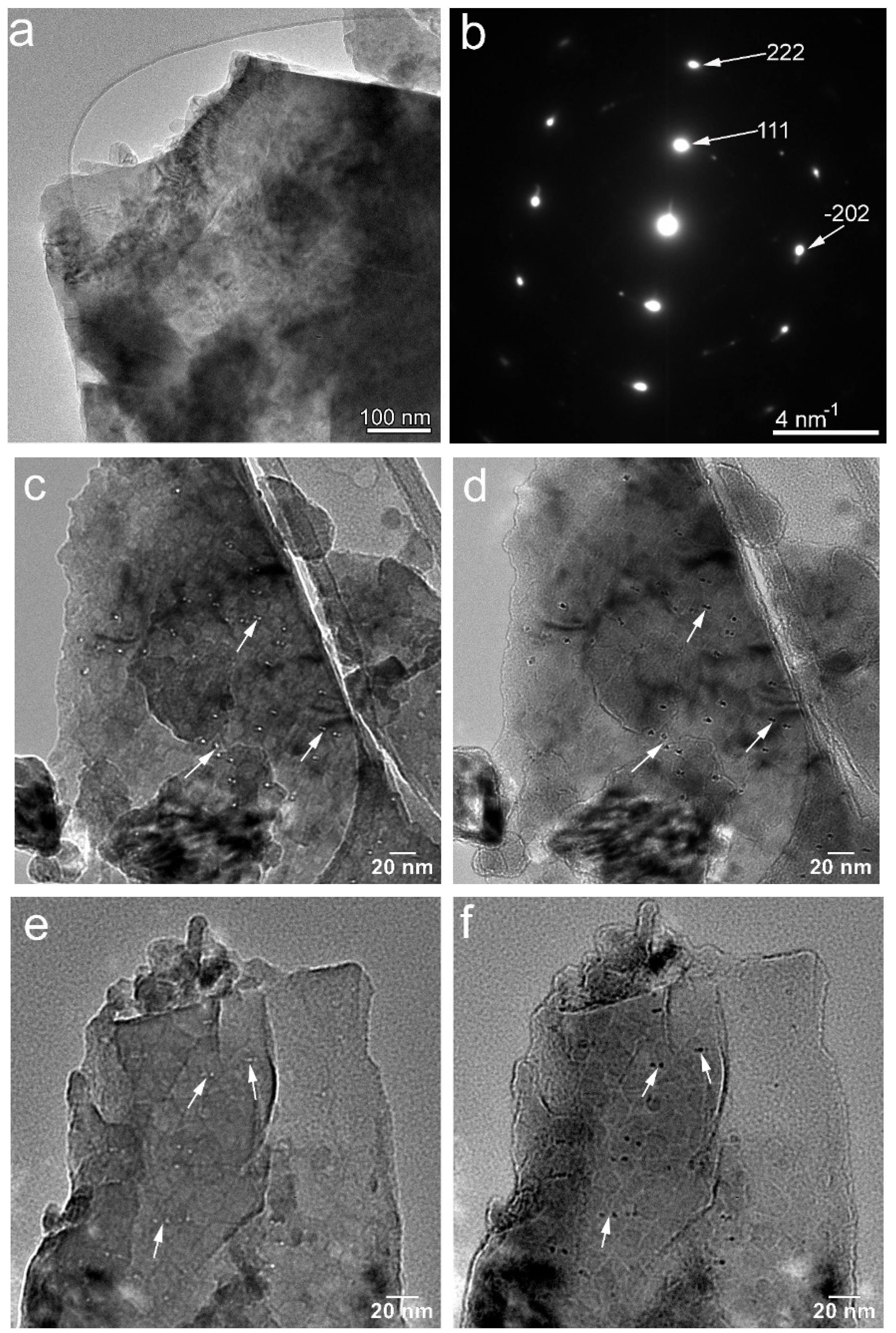
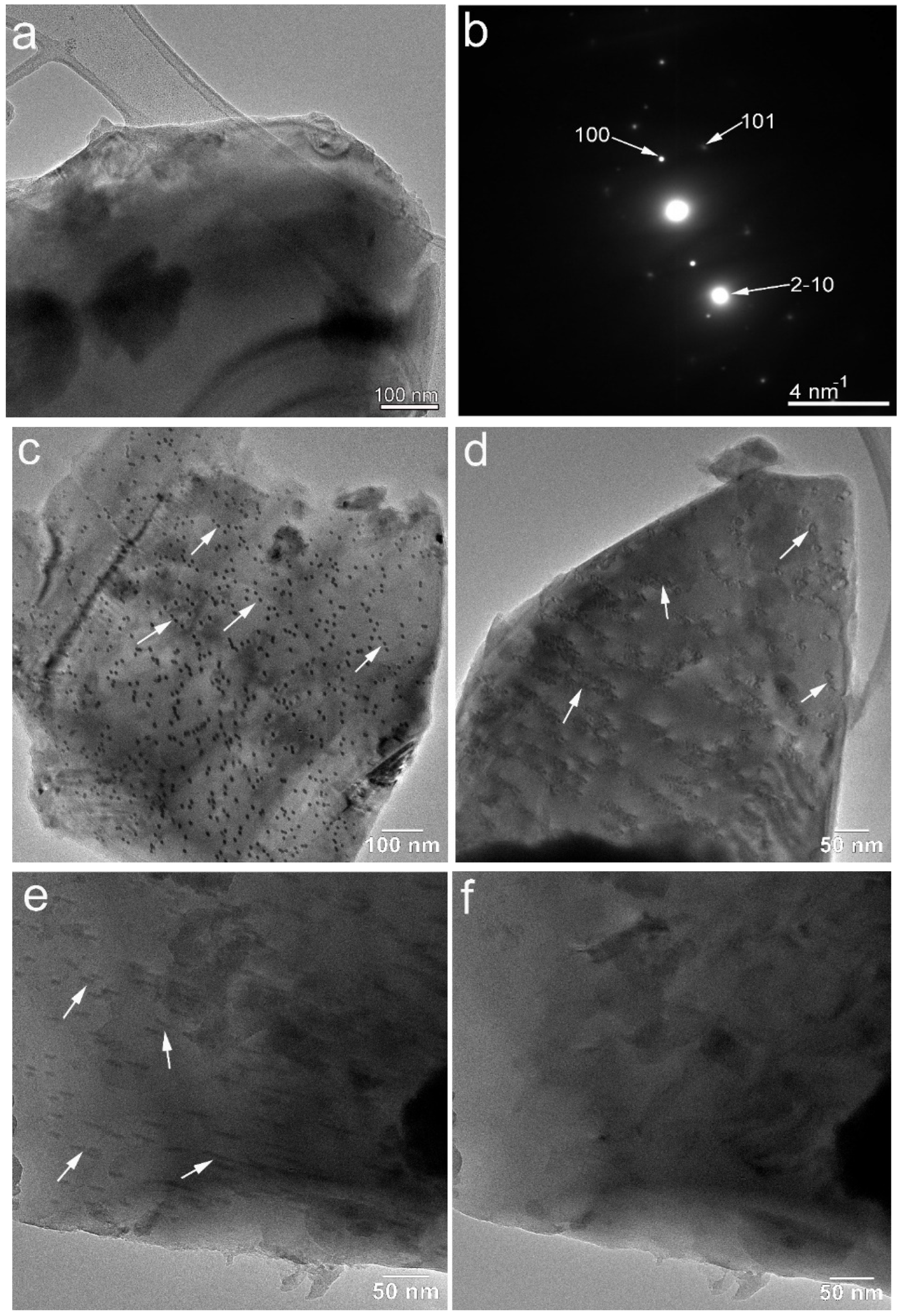
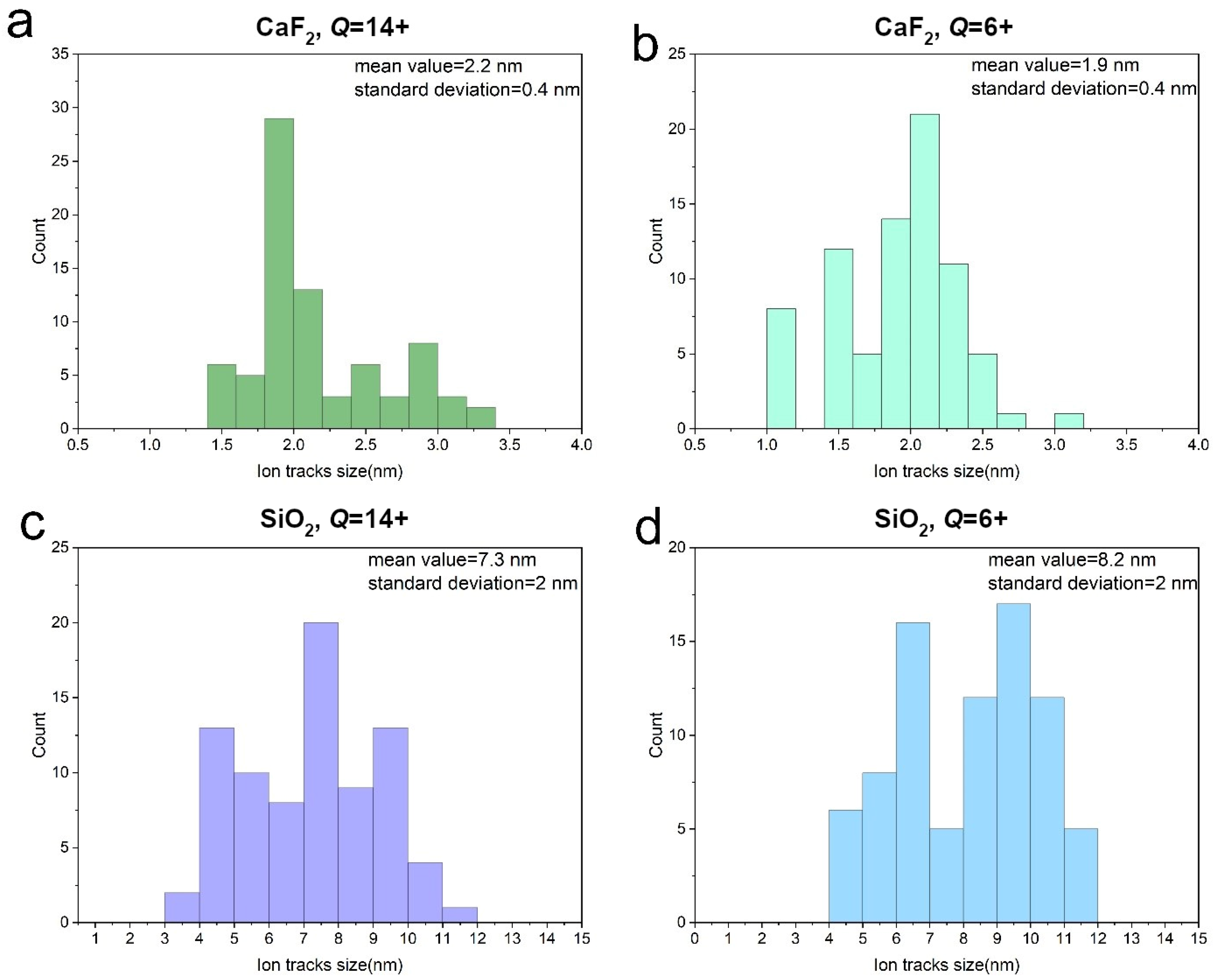
3.2. CaF2 and SiO2 Nanocrystals

In the following, we present TEM images of CaF2 and SiO2 nanocrystals irradiated with a 23 MeV I beam. Ion tracks were found in both materials, regardless of whether the thin carbon foil for charge state equilibration was used or not. Special care was taken to avoid prolonged exposure of the nanocrystals to the electron beam, as it is known that this can cause changes in the morphology of the ion track [18].
The TEM image of a typical unirradiated CaF2 crystal grain is shown in Figure 3a, together with the corresponding selected area electron diffraction (SAED) pattern close to the [1,2,3,4,5,6,7,8,9,10,11,12,13,14,15,16,17,18,19,20,21] zone axis of the FCC structure of CaF2 (Figure 3b). Next, in Figure 3c–f is shown ion tracks produced by 23 MeV I6+ irradiation, under the applied ion fluence of 1 × 10¹¹ ions/cm2. Ion tracks were produced in the absence (Figure 3c,d) and in the presence (Figure 3e,f) of the carbon foil. In order to reveal and confirm the nature of the observed nanometric features as being ion tracks, images were acquired both in under-focused (Figure 3c,e) and over-focused (Figure 3d,f) conditions. In all these cases, individual ion tracks were found, and their density matches the applied ion fluence.
In the same manner, TEM images of typical SiO2 (quartz) crystal grains before and after irradiation are shown in Figure 4. The SAED pattern shown in Figure 4b indicates the hexagonal structure of SiO2. Again, individual ion tracks (with density matching applied ion fluence) were found in all investigated cases. Finally, in Figure 4e,f, we present evidence of ion tracks fading under the prolonged exposure (typically after a few minutes) to the electron beam. A similar behaviour was also observed in the CaF2 crystal grains.
The ion track size distribution was analysed by measuring the diameter of approximately 100 ion tracks for each sample. According to the obtained histograms, fitted with a log-normal distribution, the ion tracks were found to be smaller (2–3 nm) in CaF2 (Figure 5a,b) than in quartz SiO2 (in the range of 4–10 nm, Figure 5c,d), in agreement with previous works [18,44]. As can be seen in the same figure, the ion track sizes are not affected by the presence of the thin carbon foil in front of the CaF2 sample, while in the case of the SiO2 sample, only a small difference was observed. Contrary to the expected, ion tracks appear to be larger in the SiO2 nanocrystal irradiated without the use of the carbon foil. However, this is not completely unexpected, as the wide distribution of the measured ion track sizes can contribute to this observation. Therefore, we conclude that in this type of experiment, when the nanocrystal size under investigation is in the range of several hundred nanometres, equilibration of the ion charge state does not present a sufficiently significant process whose effects would be observed by direct inspection of the ion track under the TEM.

4. Conclusions

In the present work, we have shown that the charge state of the SHI can play an important role in damage formation in monolayer graphene. Raman spectroscopy data show that much more fluence (roughly 3×) is needed for 23 MeV I6+ delivered from the accelerator to match the same amount of damage acquired in exposure to the same, but fully equilibrated, SHI beam. Further experiments studying the response of the monolayer graphene to the charge state selected SHI beams of various electronic stopping powers would be welcome.
Besides this important result, it is also of considerable interest to report the absence of charge state effects in bilayer and trilayer graphene, established by Raman spectroscopy. As mentioned before, charge state equilibration in graphene for low-energy, highly charged ions has been established for this type of target [42,43]. This is likely related to the extraordinary electronic properties of graphene, which were also previously found to be important in ion irradiation experiments [45]. Furthermore, the role of the substrate should be considered [32,36,38,39], and future experiments should include suspended graphene as a target.
Finally, no effects of the ion charge state were found in the ion tracks observed in CaF2 and SiO2 nanocrystals with TEM. Thus, it appears that recrystallisation is a more important process relevant for the near-surface variation in ion track sizes observed by the TEM [46,47,48], although this might not always be the case [49,50,51,52]. In future searches for evidence of the charge state-related effects in ion tracks within the near-surface region, experimental conditions should be tuned to (1) the vicinity of the ion track threshold (when electronic stopping might be just below the track formation threshold when SHI is not fully equilibrated) or (2) very high ion energies (when the charge state equilibration distance is comparable to the depth of the near-surface region where recrystallisation is suppressed).

Supplementary Materials

The following supporting information can be downloaded at: https://www.mdpi.com/article/10.3390/cryst12060865/s1, Figure S1: Raman spectra of bilayer graphene (BLG) irradiated with 23 MeV I using (a) charge state Q = 6+, (b) equilibrium charge state Q = 14+; Figure S2: Raman spectra of trilayer graphene (TLG) irradiated with 23 MeV I using (a) charge state Q = 6+, (b) equilibrium charge state Q = 14+; Figure S3: Raman spectra of graphite (HOPG) irradiated with 23 MeV I using (a) charge state Q = 6+ (reprinted with permission from ref. [27]), (b) equilibrium charge state Q = 14+.

Author Contributions

Conceptualization, K.T.L., J.H., M.J. and M.K.; Formal analysis, K.T.L., J.H., P.D., A.G. and C.G.M.; Funding acquisition, M.K.; Investigation, K.T.L., J.H., P.D., A.G., Z.S., C.G.M. and C.G.; Methodology, K.T.L., J.H., P.D., A.G. and M.K.; Project administration, C.G., M.J. and M.K.; Resources, C.G., M.J. and M.K.; Supervision, A.G., P.D., Z.S., C.G. and M.K.; Validation, K.T.L., J.H., A.G., P.D., Z.S. and M.K.; Visualization, K.T.L., J.H., P.D., C.G.M. and M.K.; Writing—original draft, C.G. and M.K.; Writing—review and editing, K.T.L., J.H., P.D. and C.G. All authors have read and agreed to the published version of the manuscript.

Funding

This work was supported by the Croatian Science Foundation (HrZZ project IP-2018-01-2786). The financial support from the European Regional Development Fund for the ‘Center of Excellence for Advanced Materials and Sensing Devices’ (Grant No. KK.01.1.1.01.0001), and by the FLAG-ERA project NU-TEGRAM is gratefully acknowledged. The work of doctoral student J.H. has been supported by “Young Researchers’ Career Development Project-Training of Doctoral Students” of the Croatian Science Foundation. The authors acknowledge CERIC-ERIC Consortium for the access to experimental facilities and financial support. C.G.M. and C.G. acknowledge funding through contract POC 332/390008/29.12.2020-SMIS 109522. M.J. acknowledges gratefully the support from the IAEA F11020 CRP “Ion Beam Induced Spatio-temporal Structural Evolution of Materials: Accelerators for a New Technology Era”. We acknowledge support by the Croatian-Austrian bilateral project financed by the OAED GmbH, Austria and Ministry of Science and education of Croatia.

Institutional Review Board Statement

Not applicable.

Informed Consent Statement

Not applicable.

Data Availability Statement

Data is available on request.

Conflicts of Interest

The authors declare no conflict of interest.

References

  1. Krasheninnikov, A.V.; Nordlund, K. Ion and electron irradiation-induced effects in nanostructured materials. J. Appl. Phys. 2010, 107, 071301. [Google Scholar] [CrossRef]
  2. Krasheninnikov, A.V. Are two-dimensional materials radiation resistant? Nanoscale Horiz. 2020, 5, 1447. [Google Scholar] [CrossRef] [PubMed]
  3. Facsko, S.; Dekorsy, T.; Koerdt, C.; Trappe, C.; Kurz, H.; Vogt, A.; Hartnagel, H.L. Formation of ordered nanoscale semiconductor dots by ion sputtering. Science 1999, 285, 1551–1553. [Google Scholar] [CrossRef] [Green Version]
  4. Bogdanović-Radović, I.; Buljan, M.; Karlušić, M.; Skukan, N.; Božičević, I.; Jakšić, M.; Radić, N.; Dražić, G.; Bernstorff, S. Conditions for formation of germanium quantum dots in amorphous matrices by MeV ions: Comparison with standard thermal annealing. Phys. Rev. B 2012, 86, 165316. [Google Scholar] [CrossRef]
  5. Lotito, V.; Karlušić, M.; Jakšić, M.; Tomić Luketić, K.; Müller, U.; Zambelli, T.; Fazinić, S. Shape Deformation in Ion Beam Irradiated Colloidal Monolayers: An AFM Investigation. Nanomaterials 2020, 10, 453. [Google Scholar] [CrossRef] [Green Version]
  6. Madauß, L.; Schumacher, J.; Ghosh, M.; Ochedowski, O.; Meyer, J.; Lebius, H.; Ban-d’Etat, B.; Tomil-Molares, M.E.; Trautmann, C.; Lammertink, R.G.H.; et al. Fabrication of Nanoporous Graphene/Polymer Composite Membranes. Nanoscale 2017, 9, 10487. [Google Scholar] [CrossRef]
  7. Akcöltekin, E.; Peters, T.; Meyer, R.; Duvenbeck, A.; Klusmann, M.; Monnet, I.; Lebius, H.; Schleberger, M. Creation of multiple nanodots by single ions. Nat. Nanotechnol. 2007, 2, 290–294. [Google Scholar] [CrossRef] [Green Version]
  8. Akcöltekin, S.; Bukowska, H.; Peters, T.; Osmani, O.; Monnet, I.; Alzaher, I.; Ban-d’Etat, B.; Lebius, H.; Schleberger, M. Unzipping and folding of graphene by swift heavy ions. Appl. Phys. Lett. 2011, 98, 103103. [Google Scholar] [CrossRef]
  9. Karlušić, M.; Mičetić, M.; Kresić, M.; Jakšić, M.; Šantić, B.; Bogdanović-Radović, I.; Bernstorff, S.; Lebius, H.; Ban-d’Etat, B.; Rožman, K.Ž.; et al. Nanopatterning surfaces by grazing swift heavy ion irradiation. Appl. Surf. Sci. 2021, 541, 148467. [Google Scholar] [CrossRef]
  10. Vázquez, H.; Kononov, A.; Kyritsakis, A.; Medvedev, N.; Schleife, A.; Djurabekova, F. Electron cascades and secondary electron emission in graphene under energetic ion irradiation. Phys. Rev. B 2021, 103, 224306. [Google Scholar] [CrossRef]
  11. Rymzhanov, R.; Medvedev, N.; Volkov, A.E. Damage kinetics induced by swift heavy ion impacts onto films of different thicknesses. Appl. Surf. Sci. 2021, 566, 150640. [Google Scholar] [CrossRef]
  12. Iveković, D.; Žugec, P.; Karlušić, M. Energy Retention in Thin Graphite Targets after Energetic Ion Impact. Materials 2021, 14, 6289. [Google Scholar] [CrossRef] [PubMed]
  13. Schiwietz, G.; Czerski, K.; Roth, M.; Staufenbiel, F.; Grande, P.L. Femtoseconddynamics-snapshots of the early ion track evolution. Nucl. Instrum. Meth. Phys. Res. B 2004, 225, 4–26. [Google Scholar] [CrossRef]
  14. Toulemonde, M. Irradiation by swift heavy ions: Influence of the non-equilibrium projectile charge state for near surface experiments. Nucl. Instrum. Methods Phys. Res. Sect. B 2006, 250, 263–268. [Google Scholar] [CrossRef]
  15. Aumayr, F.; Facsko, S.; El-Said, A.S.; Trautmann, C.; Schleberger, M. Single ion induced surface nanostructures: A comparison between slow highly charged and swift heavy ions. J. Phys. Condens. Matter. 2011, 23, 393001. [Google Scholar] [CrossRef] [Green Version]
  16. Schleberger, M.; Kotakoski, J. 2D Material Science: Defect Engineering by Particle Irradiation. Materials 2018, 11, 1885. [Google Scholar] [CrossRef] [Green Version]
  17. Rymzhanov, R.; Medvedev, N.; O’Connell, J.H.; Janse van Vuuren, A.; Skuratov, V.A.; Volkov, A.E. Recrystallization as the governing mechanism of ion track formation. Sci. Rep. 2019, 9, 3837. [Google Scholar]
  18. Karlušić, M.; Ghica, C.; Negrea, R.F.; Siketić, Z.; Jakšić, M.; Schleberger, M.; Fazinić, S. On the threshold for ion track formation in CaF2. New J. Phys. 2017, 19, 023023. [Google Scholar] [CrossRef] [Green Version]
  19. Siketić, Z.; Bogdanović-Radović, I.; Jakšić, M.; Skukan, N. Time of flight elastic recoil detection analysis with a position sensitive detector. Rev. Sci. Instr. 2010, 81, 03305. [Google Scholar] [CrossRef]
  20. Grande, P.; Schiwietz, G. Impact-parameter dependence of the electronic energy loss of fast ions. Phys. Rev. A 1998, 58, 3796. [Google Scholar] [CrossRef] [Green Version]
  21. Ziegler, J.F.; Ziegler, M.D.; Biersack, J.P. SRIM–the stopping and range of ions in the matter (2010). Nucl. Instr. Meth. B 2010, 268, 1818. [Google Scholar] [CrossRef] [Green Version]
  22. Wilhelm, R.A.; Möller, W. Charge-state-dependent energy loss of slow ions. II. Statistical atom model. Phys. Rev. A 2016, 93, 052709. [Google Scholar] [CrossRef]
  23. Nečas, D.; Klapetek, P. Gwyddion: An open-source software for SPM data analysis. Cent. Eur. J. Phys. 2012, 10, 181. [Google Scholar] [CrossRef]
  24. Matthew, S.; Chan, T.K.; Zhan, D.; Gopinadhan, K.; Barman, A.-R.; Breese, M.B.H.; Dhar, S.; Shen, Z.X.; Venkatesan, T.; Thong, J.T.L. The effect of layer number and substrate on the stability of graphene under MeV proton beam irradiation. Carbon 2011, 49, 1720–1726. [Google Scholar] [CrossRef] [Green Version]
  25. Lucchese, M.M.; Stavale, F.; Ferreira, E.H.M.; Vilani, C.; Moutinho, M.V.O.; Capaz, R.B.; Achete, C.A.; Jorio, A. Quantifying ion-induced defects and Raman relaxation length in graphene. Carbon 2010, 48, 1592–1597. [Google Scholar] [CrossRef]
  26. Zeng, J.; Yao, H.J.; Zhang, S.X.; Zhai, P.F.; Duan, J.L.; Sun, Y.M.; Li, G.P.; Liu, J. Swift heavy ions induced irradiation effects in monolayer graphene and highly oriented pyrolytic graphite. Nucl. Instr. Meth. Phys. Res. B 2014, 330, 18. [Google Scholar] [CrossRef]
  27. Zeng, J.; Liu, J.; Yao, H.J.; Zhai, P.F.; Zhang, S.X.; Guo, H.; Hu, P.P.; Duan, J.L.; Mo, D.; Hou, M.D.; et al. Comparative study of irradiation effects in graphite and graphene. Carbon 2016, 100, 16–26. [Google Scholar] [CrossRef] [Green Version]
  28. Tomić Luketić, K.; Karlušić, M.; Gajović, A.; Fazinić, S.; O’Connell, J.H.; Pielić, B.; Radatović, B.; Kralj, M. Investigation of Ion Irradiation Effects in Silicon and Graphite Produced by 23 MeV I Beam. Materials 2021, 14, 1904. [Google Scholar] [CrossRef]
  29. Ochedowski, O.; Lehtinen, O.; Kaiser, U.; Turchanin, A.; Ban-d’Etat, B.; Lebius, H.; Karlušić, M.; Jakšić, M.; Schleberger, M. Nanostructuring Graphene by Dense Electronic Excitation. Nanotechnology 2015, 26, 465302. [Google Scholar] [CrossRef] [Green Version]
  30. Karlušić, M.; Rymzhanov, R.A.; O’Connell, J.H.; Bröckers, L.; Tomić Luketić, K.; Siketić, Z.; Fazinić, S.; Dubček, P.; Jakšić, M.; Provatas, G.; et al. Mechanisms of surface nanostructuring of Al2O3 and MgO by grazing incidence irradiation with swift heavy ions. Surf. Interf. 2021, 27, 101508. [Google Scholar] [CrossRef]
  31. Hanžek, J.; Dubček, P.; Fazinić, S.; Tomić Luketić, K.; Karlušić, M. High-Energy Heavy Ion Irradiation of Al2O3, MgO and CaF2. Materials 2022, 15, 2110. [Google Scholar] [CrossRef] [PubMed]
  32. Vázquez, H.; Ahlgren, E.H.; Ochedowski, O.; Leino, A.A.; Mirzayev, R.; Kozubek, R.; Lebius, H.; Karlušić, M.; Jakšić, M.; Krasheninnikov, A.V.; et al. Creating nanoporous graphene with swift heavy ions. Carbon 2017, 114, 511. [Google Scholar] [CrossRef] [Green Version]
  33. Khalfaoui, N.; Rotaru, C.C.; Bouffard, S.; Toulemonde, M.; Stoquert, J.P.; Haas, F.; Trautmann, C.; Jensen, J.; Dunlop, A. Characterization of swift heavy ion tracks in CaF2 by scanning force and transmission electron microscopy. Nucl. Instrum. Methods Phys. Res. Sect. B 2005, 240, 819–828. [Google Scholar] [CrossRef]
  34. Karlušić, M.; Jakšić, M.; Lebius, H.; Ban-d’Etat, B.; Wilhelm, R.A.; Heller, R.; Schleberger, M. Swift heavy ion track formation in SrTiO3 and TiO2. J. Phys. D Appl. Phys. 2017, 50, 205302. [Google Scholar] [CrossRef]
  35. Ogawa, T.; Ishikawa, N.; Kai, T. Depth profiles of energy deposition near incident surface irradiated with swift heavy ions. Nucl. Instrum. Methods Phys. Res. Sect. B 2019, 461, 272–275. [Google Scholar] [CrossRef]
  36. Zhao, S.; Xue, Y.; Wang, Y.; Yan, S. Effect of SiO2 substrate on the irradiation-assisted manipulation of supported graphene-a molecular dynamics study. Nanotechnology 2012, 23, 285703. [Google Scholar] [CrossRef] [PubMed]
  37. Kretschmer, S.; Maslow, M.; Ghaderzadeh, S.; Ghorbani-Asl, M.; Hlawaczek, G.; Krasheninnikov, A. Supported two-dimensional materials under ion irradiation: The substrate governs defect productions. ACS Appl. Mater. Interfaces 2018, 10, 30827. [Google Scholar] [CrossRef]
  38. Zhao, S.; Xue, Y. Modification of graphene supported on SiO2 substrate with swift heavy ions from atomistic simulation point. Carbon 2015, 93, 169. [Google Scholar] [CrossRef]
  39. Li, W.; Wang, X.; Zhang, X.; Zhao, S.; Duan, H.; Xue, J. Mechanism of the Defect Formation in Supported Graphene by Energetic Heavy Ion Irradiation: The Substrate Effect. Sci. Rep. 2015, 5, 9935. [Google Scholar] [CrossRef] [Green Version]
  40. Toulemonde, M.; Assmann, W.; Trautmann, C. Electronic sputtering of vitreous SiO2: Experimental and modelling results. Nucl. Instr. Meth. Phys. Res. B 2016, 379, 2. [Google Scholar] [CrossRef]
  41. Matthew, S.; Chan, T.K.; Zhan, D.; Gopinadhan, K.; Barman, A.R.; Breese, M.B.H.; Dhar, S.; Shen, Z.X.; Venkatesan, T.; Thong, J.T.L. Mega-electron-volt proton irradiation on supported and suspended graphene: A Raman spectroscopic layer dependent study. J. Appl. Phys. 2011, 110, 084309. [Google Scholar] [CrossRef] [Green Version]
  42. Niggas, A.; Creutzburg, S.; Schwestka, J.; Wöckinger, B.; Gupta, T.; Grande, P.L.; Eder, D.; Marques, J.P.; Bayer, B.C.; Aumayr, F.; et al. Peeling graphite layer by layer reveals the charge exchange dynamics of ions inside a solid. Commun. Phys. 2021, 4, 180. [Google Scholar] [CrossRef]
  43. Creutzburg, S.; Niggas, A.; Weichselbaum, D.; Grande, P.L.; Aumayr, F.; Wilhelm, R.A. Angle-dependent charge exchange and energy loss of slow highly charged ion in freestanding graphene. Phys. Rev. A 2021, 104, 042806. [Google Scholar] [CrossRef]
  44. Pena-Rodríguez, O.; Manzano-Santamaría, J.; Rivera, A.; García, G.; Olivares, J.; Agulló-López, F. Kinetics of amorphization induced by swift heavy ions in alpha-quartz. J. Nucl. Mater. 2012, 430, 125–131. [Google Scholar] [CrossRef] [Green Version]
  45. Gruber, E.; Wilhelm, R.A.; Pétuya, R.; Smejkal, V.; Kozubek, R.; Hierzenberger, A.; Bayer, B.; Aldazabal, I.; Kazansky, A.K.; Libisch, F.; et al. Ultrafast electronic response of graphene to a strong and localized electric field. Nat. Commun. 2016, 7, 13948. [Google Scholar] [CrossRef] [PubMed] [Green Version]
  46. O’Connell, J.H.; Skuratov, V.A.; Akilbekov, A.; Zhumazhanova, A.; Janse van Vuuren, A. EM study of latent ion track morphology in TiO2 single crystals. Nucl. Instr. Meth. Phys. Res. B 2016, 379, 200–205. [Google Scholar] [CrossRef]
  47. Zhai, P.; Nan, S.; Xu, L.; Li, W.; Li, Z.; Hu, P.; Zeng, J.; Zhang, S.; Sun, Y.; Liu, J. Fine structure of swift heavy ion track in rutile TiO2. Nucl. Instr. Meth. Phys. Res. B 2019, 457, 72–79. [Google Scholar] [CrossRef] [Green Version]
  48. Ishikawa, N.; Taguchi, T.; Ogawa, H. Comprehensive Understanding of Hillocks and Ion Tracks in Ceramics Irradiated with Swift Heavy Ions. Quantum Beam Sci. 2020, 4, 43. [Google Scholar] [CrossRef]
  49. Kamarou, A.; Wendler, E.; Wesch, W. Charge state effect on near-surface damage formation in swift heavy ion irradiated InP. J. Appl. Phys. 2005, 97, 123532. [Google Scholar] [CrossRef]
  50. Gupta, S.; Gehrke, H.G.; Krauser, J.; Trautmann, C.; Severin, D.; Bender, M.; Rothard, H.; Hofsäss, H. Conducting ion tracks generated by charge-selected swift heavy ions. Nucl. Instr. Meth. Phys. Res. B 2016, 381, 76–83. [Google Scholar] [CrossRef]
  51. Alencar, I.; Silva, M.R.; Leal, R.; Grande, P.L.; Papaleo, R.M. Impact Features Induced by Single Fast Ions of Different Charge-State on Muscovite Mica. Atoms 2021, 9, 17. [Google Scholar] [CrossRef]
  52. Matsunami, N.; Sataka, M.; Okayasu, S.; Tsuchiya, B. Charge State Effect of High Energy Ions on Material Modification in the Electronic Stopping Region. Atoms 2021, 9, 36. [Google Scholar] [CrossRef]
Figure 1. (a) Raman spectra of the monolayer graphene irradiated with 23 MeV iodine beam and charge state Q = 6+, with fluences between 5 × 10¹² and 5 × 10¹³ ions/cm2. For comparison, a spectrum from unirradiated graphene is also added. (b) Raman spectra of the monolayer graphene irradiated with 23 MeV iodine beam and equilibrium charge state Q = 14+, with fluences between 5 × 10¹² and 5 × 10¹³ ions/cm2. For comparison, a spectrum from unirradiated graphene is also added. (c) Comparison of Raman spectra for monolayer graphene irradiated with 23 MeV I beam at the fluence of 5 × 10¹² ions/cm2 with the charge state of Q = 6+ and Q = 14+. (d) Ratio of the peak intensities ID/IG as a function of the applied ion fluence and charge state Q for monolayer graphene (blue), bilayer graphene (green), trilayer graphene (orange), and HOPG (black).
Crystals 12 00865 g001aCrystals 12 00865 g001bCrystals 12 00865 g001cCrystals 12 00865 g001d
Figure 2. (a) AFM images of the graphene surface before irradiation, (b) after irradiation with a charge state of Q = 6+ and (c) after irradiation with equilibrium charge state, both with the same 5 × 10¹³ ions/cm2 fluence. The images have the same false colour vertical scale range of 3 nm.
Crystals 12 00865 g002aCrystals 12 00865 g002b
Figure 3. TEM image (a) and corresponding SAED pattern (b) revealing the FCC structure of the unirradiated CaF2 nanocrystals. Under-focused (c) and over-focused (d) TEM images of the CaF2 nanocrystals irradiated with 23 MeV I at the fluence of 1 × 10¹¹ ions/cm2 with charge state of Q = 6+. Under-focused (e) and over-focused (f) TEM images of the CaF2 nanocrystals irradiated with 23 MeV I at the fluence of 1 × 10¹¹ ions/cm2 with the equilibrated charge state.
Crystals 12 00865 g003
Figure 4. TEM image (a) and corresponding SAED pattern (b) revealing the hexagonal structure of the unirradiated SiO2 nanocrystals. Over-focused TEM image (c) of the SiO2 nanocrystals irradiated with 23 MeV I at the fluence of 1 × 10¹¹ ions/cm2 with charge state of Q = 6+. Over-focused TEM image (d) of the SiO2 nanocrystals irradiated with 23 MeV I at the fluence of 1 × 10¹¹ ions/cm2 with the equilibrated charge state. Ion tracks in SiO2 pointed by arrows in (e) fade away and disappear after prolonged exposure to the electron beam (f).
Crystals 12 00865 g004
Figure 5. Distribution of the ion track diameters in CaF2 nanocrystals irradiated with 23 MeV I at the fluence of 1 × 10¹¹ ions/cm2 with (a) equilibrated charge state and (b) charge state of Q = 6+. Distribution of the ion track diameters in SiO2 nanocrystals irradiated with 23 MeV I at the fluence of 1 × 10¹¹ ions/cm2 with (c) equilibrated charge state and (d) charge state of Q = 6+.
Crystals 12 00865 g005
Table 1. The 23 MeV I irradiation parameters calculated by CasP 5.2 [20] and SRIM 2013 codes [21].
Material
and
Density
(g/cm3)
Electronic Stopping
CasP: Q = 6+
(keV/nm)
Electronic Stopping CasP: Q = 14+
(keV/nm)
Electronic Stopping SRIM
(keV/nm)
Nuclear Stopping SRIM
(keV/nm)
Ion Range SRIM
(μm)
Graphite
(2.25)
4.36.66.70.275.55
a-SiO2
(2.2)
3.74.85.20.267.19
CaF2
(3.18)
4.75.96.40.355.91
Quartz SiO2
(2.65)
4.45.86.30.315.97
Publisher’s Note: MDPI stays neutral with regard to jurisdictional claims in published maps and institutional affiliations.

