
Lithographically Ordered FePt L10 Dots with High Coercivity for Logic-Conditioned Magnetic Nanostructures
National Institute for Materials Physics, P.O. Box MG-7, 077125 Magurele, Romania
*
Author to whom correspondence should be addressed.
Crystals 2024, 14(1), 58; https://doi.org/10.3390/cryst14010058
Submission received: 10 November 2023
/
Revised: 19 December 2023
/
Accepted: 27 December 2023
/
Published: 31 December 2023
(This article belongs to the Topic Advanced Magnetic Alloys)
Abstract
:In order to develop the building blocks for future biosensing and spintronic applications, an engraving technique using electron beam lithography is employed in order to develop nanomagnetic pre-patterned structures with logic potential. The paper describes the realization and morphological and magnetic characterization of potentially logic-conditioned substrates, a building block to be further used as an integration platform upon which nanodevices, such as magnetic wires, or various geometrical shapes, circles, triangles, can be considered as pre-requisite for full integration into logic devices. As a proof of concept, regular arrays of FePt circles or magnetic dots were devised and structural characterization by X-ray diffraction and transmission electron microscopy proved the occurrence of the tetragonal L10 phase. Moreover, the magnetic characterization provided more insight into the potential of such arrays of magnetic devices as the hysteresis provided good values of magnetic coercivity, remanent and saturation magnetization. These findings show good potential for developing regular arrays of uniformly shaped magnetic entities with encouraging magnetic performances in view of potential applications in various applications.
1. Introduction
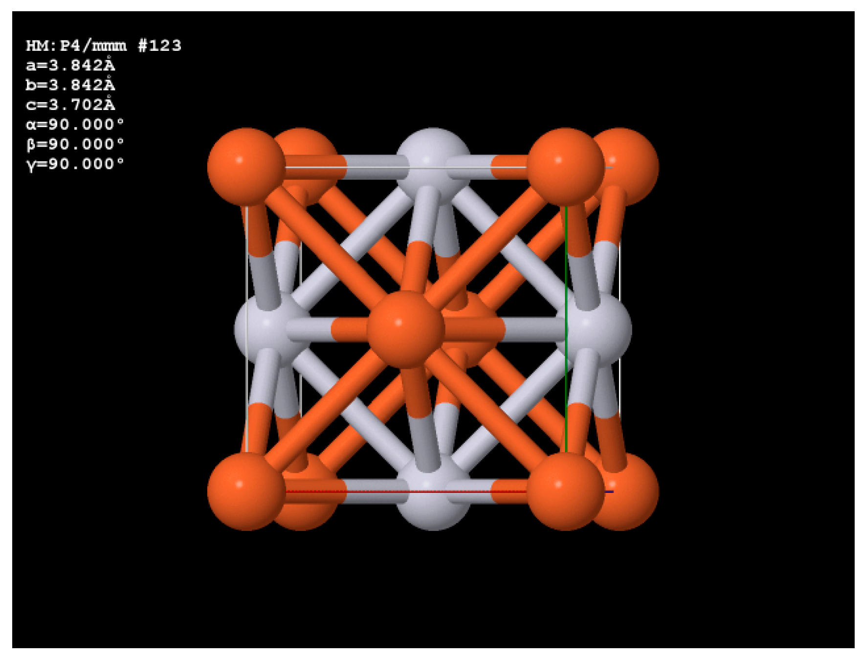
There has been a surge of interest in the investigation of size-dependent phenomena, as a response to the industry needs for highly performant nanodevices. The recent award of the Nobel Prize in Chemistry 2023 to the pioneers of the development of quantum dot fabrication [1] shows how important and real the study of size-dependent phenomena is at the nano scale. One phenomenon of particular interest is that of magnetic dots, or nanostructures that are suitable for spintronic applications as well as for heating dot magnetic recording (HDMR). The formation of hybrid nanostructures in spintronic devices has been recently investigated [2] as a response to specific needs, especially in nanodiagnostics, nanoelectronics and in adjacent fields where combined optical and magnetic response to various excitations is required for various types of sensing. With the advent of high accuracy and high-resolution fabrication technologies, such as lithography, coupling phenomena at the nanoscale for magnetic dots and for arrays of dots may become accessible. The integration of the magnetic and semiconductor components adds new capabilities to electronic devices [3]. While spin phenomena have long been investigated within the context of conventional ferromagnetic materials, the study of spin generation, relaxation, and spin–orbit coupling in non-magnetic materials has taken off only recently, with the advent of hybrid spintronics and it is here that many novel materials and architectures can find their greatest potential in both science and technology. Additionally, the heating dot magnetic recording (HDMR) principle, derived from heat-assisted magnetic recording (HAMR) has been shown to be a targeted application in instances where a key system is represented by FePt nanoclusters [4,5]. In this view, Mohan et al. [4] and Medwal et al. [5] have proposed the fabrication of self-stabilized FePt non-stoichiometric clusters by a chemical route, i.e., reduction using oleic acid and oleylamine. An annealing at 600 °C transformed these FePt colloidal nanoparticles into carbon-coated L10 FePt phase nanoclusters. As proposed by Seagate a number of years ago [6], the heated dot magnetic recording (HDMR) is a promising technology suitable for increasing the density of media used for magnetic recording to values of around 4 Tb/in2. It is indeed true that the heating dot magnetic recording technology needs arrays of magnetic dots that are periodically dispersed, non-interacting, well within the nanometer-size range, and that have a stable magnetic response and high uniaxial perpendicular magnetic anisotropy. While the chemical route described in [4,7] provides non-interacting, small nanoparticles, their carbonaceous coating can impede the recording processes due to the diminishing of the magnetic response. The lithographical route proposed in [6] has the advantage of providing regular disposal of these small nanoclusters. Here, the media is made of a continuously deposited FePt film and lithographical path is employed to provide and define regular arrays of periodically disposed magnetic dots which are subsequently heated to achieve the L10 FePt phase. It is to be noted that the L10 phase is considered as a high order tetragonal distortion of the FePt cubic phase where the unit cell consists of planes of only Fe atoms stacked over slabs of only Pt atoms as in Figure 1:
A systematic study on the size dependence of the coercivity in FePt magnetic dots has been developed in [8,9]. In these works, FePt nanodot arrays were lithographically patterned and their magnetic properties were investigated using the technique of X-ray magnetic circular dichroism combined with magneto-optic Kerr effect (MOKE) magnetometry. It has been shown that magnetic dots between 30 and 100 nm exhibit coercivity increase upon annealing at quite high temperatures [9]; however, it has been found that not all of the dots achieve the L10 FePt phase. As a consequence, the amount of untransformed magnetic dots, which remained in the disordered, A1 FePt cubic, soft magnetic phase, causes a degradation of the overall perpendicular magnetic anisotropy.
Pre-patterning of the magnetic media is also one of the solutions developed for biosensing, using integrated platforms and arrays of sensors where the detection is guided by magneto-transport phenomena. For instance, pre-patterned media was used to prove the efficiency of giant magnetoresistance (GMR) spin valve sensors designed for the detection of superparamagnetic nanoparticles as potential biomolecular labels in magnetic biodetection technology [10]. In this example a patterned self-assembly method, involving a polymer-mediated process via e-beam lithography, was used.
In a recent review on hybrid spintronic materials [2], systems based on ferromagnetic metals and alloys combined with semiconducting materials, are shown to receive great attention due to their potential use as spintronic materials for electronic transport and magnetic storage. Spintronic or spin-based memory (STT-RAM) [3], may revolutionize memory technology, due to its potential to combine the low cost of DRAM, the speed of SRAM, and the non-volatility of flash, and has virtually no static energy consumption. A major breakthrough that has the potential to allow improvement of the write speed and power of such spintronic memory is the recently reported magnetization reversal by femtosecond laser pulses in thin ferromagnetic Gd/Fe/Co films [11,12]. Conceptually, this represents a new way to control the magnetic state of a medium, at the highest efficiency and shortest possible timescale. Recent results show that the phenomenon extends also to rare-earth free transition metal multilayers and that Co/Ir heterostructures [13] may have the magnetization reversed in that way. Magnetization reversal by optical means can be achieved using a laser in the femtosecond regime. Femtosecond magnetic switching has the astounding capacity to push the limit of data transfer rates to the terabit-per-second range in magnetic recording [14]. Recently integrated magnetic/spintronic device microarrays have demonstrated great potential in both biomedical research and in practices [15] where the physical mechanisms of spintronic devices for magnetic signal sensing, including giant magnetoresistance (GMR) spin valve sensors and tunnel magnetoresistance (TMR) sensors, were studied. Magnetoresistance (MR)-based biosensors are considered promising candidates for the detection of magnetic nanoparticles (MNPs) as biomarkers and biomagnetic fields. MR biosensors have been widely used in the detection of proteins and DNAs and in the mapping of cardiovascular and brain signals [16]. A more recent review on advances in magnetoresistance biosensors has been published by C. Dey et al. [17].
With the advent of more possibilities of the manipulation of spin in such magnetic dots, coupled with the nanolithography potential, there is high potential to make nanodevices an alternative to the presently employed sensors, in a way that is low-power, low-cost, easier to manufacture and is more sensitive than the current state of the art [16].
The current paper describes the realization and morphological characterization of a logic-conditioned substrate, a building block to be further used as an integration platform upon which nanodevices, such as magnetic wires or various geometrical shapes, circles, and triangles, can be considered as pre-requisite for full integration into logic devices. Moreover, arrays of magnetic dots made of non-stoichiometric L10 FePt are fabricated on these substrates, with various geometries and suitable for both bio-sensing and, potentially, for HDMR applications. Magnetization switching and measurable magnetoresistance effects can be recorded in such devices.
2. Materials and Methods
2.1. Method of Pre-Patterning and Magnetic Elements Nanofabrication
The building block needed for the integration platform was made by using electron beam lithography and photo-lithography techniques. The devices are fabricated in a dedicated class 1000 cleanroom of about 50 m2, of which a section of 15 m2 is dedicated to photolithography and has class 100 standards. The fabrication tool used was a Raith150 Two high resolution e-beam lithography machine, dotted with wet etch cabinets for acids and bases/solvents, a photolithography cabinet with PC-controlled spinner and hot plates, a mask aligner EVG 620 NT and a scanning electron microscopy SEM Hitachi S3400 with laser interferometer positioning stage from Raith (Raith GmbH, Dortmund, Germany). The aim of the processing procedure was to obtain nanostructures with specific shapes and geometries. We performed, in this respect, a dose test using the electron beam lithography technique. For this purpose, two photo-resist layers were applied on a Si(111) substrate with a native SiO2 protective layer grown on top. The first photo-resist layer applied was methyl methacrylate (MMA EL10), with a thickness of 400 nm. The second layer applied was poly-methyl methacrylate (PMMA A3) with a thickness of 100 nm. Each layer was deposited via spin-coating for 60 s, at a speed of 4000 rpm and acceleration of 500 rpm/s. After the deposition of each layer, the sample was heated at 175 °C for 10 s in order to evaporate the solvent. Nanofabrication of the magnetic element considered, in the first instance, Pt wires of various dimensions, ranging from 50 to 200 nm thickness and 7 µm length. The engraving of the wires was realized via electron beam lithography using a current of 11 pA. The size of the electron beam was 2 nm, whereas the field magnification was 800×. It is known that, in electron beam lithography, the resist performance in terms of exposure dose latitude, sensitivity, contrast, roughness and resolution, are influenced by the nature of the resist, the developer type and composition, and the development technique. In our case the dose was incremented with 0.1 μC/cm2 starting from 0.6 μC/cm2 and ending at 0.79 μC/cm2. The development was realized by keeping the sample in a solution of methyl isobutyl ketone (MiBK) and isopropyl alcohol (IPA) (1:3) for 8 s and then in IPA for 1 min. Finally, the sample was dried with nitrogen gas flow. After the development, the reactive ion etching technique was implemented in order to have a better definition of the patterned shapes. A 10 s reactive ion etching process was realized in the dedicated UHV chamber at a pressure of 15 mbar.
A layer of Pt with 30 nm thickness was deposited over the wire structure followed by a layer of Fe with 40 nm thickness. The deposition rate in the case of Pt was 0.25 nm/s, whereas the value corresponding to Fe deposition was 0.19 nm/s. The working pressure inside the deposition chamber was 10−7 mbar. The lift-off process was realized by placing the sample in acetone for 2 min at 50 °C and, afterwards, in acetone at room temperature for 30 min. After the removal of the photoresist, the nanostructure was annealed at 450 °C for 30 min in order to promote the formation of the L10 FePt phase.
2.2. Characterization Methods
Several investigation techniques are used to study the structural and morphological effects on the microstructure of the dots and the changes induced in it by annealing treatments. Additionally, a thorough study of magnetic properties after annealing as a function of applied field is performed. These studies are undertaken using X-ray diffraction (XRD), scanning electron microscopy (SEM) and high-resolution transmission electron microscopy (HRTEM) coupled to selected area electron diffraction (SAED) and magnetic characterizations. For XRD, a Bruker D8 Advance (Bruker AXS GmbH, Karlsruhe, Germany) with Cu Kα radiation wavelength of 1.54 Å was used. For the SEM imaging, Lyra 3XMU with a Focused Ion Beam SEM-FIB sample preparation stage, from Tescan (Tescan France, Fuveau, France) was used. The facility is equipped with secondary electron detectors with a resolution of 5 nm at 30 kV. Transmission electron microscopy in high resolution mode was recorded using a JEM ARM 200 F electron microscope operated at 200 kV acceleration voltage, from JEOL (JEOL Ltd., Hertfordshire, UK). Magnetic characterization was performed with a superconducting quantum interference device (SQUID) unit of a magnetic properties measurement system (MPMS) from Quantum Design (Quantum Design Europe GmbH, Darmstadt, Germany), under a magnetic applied field of up to 5 Tesla. Measurements were taken both in parallel but also in perpendicular geometry and with temperatures ranging from 5 K to 300 K. The parallel and perpendicular refers to the direction of the applied magnetic field with respect to the array plane.
3. Results
3.1. Complex Morphology Analysis
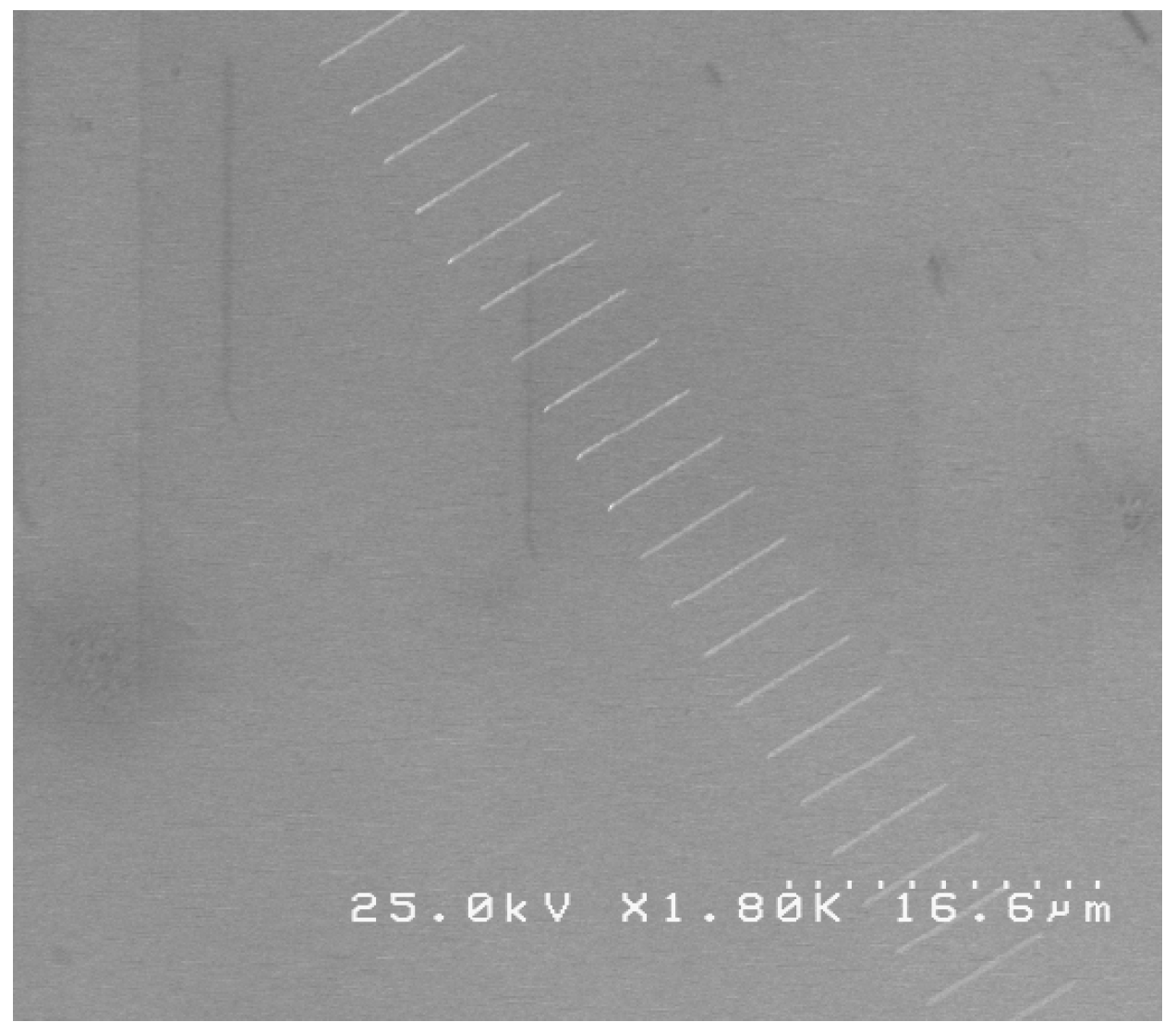
Scanning electron microscopy (SEM) images of the obtained nanostructures were collected. The first set of deposited wires, with a real thickness of approximately 200 nm were deposited in a sequence of exposure doses ranging from 0.6 μC/cm2 up to 0.79 μC/cm2. The SEM image presented in Figure 2 exhibits these traits, wherein the doses increase from the top of the image to the bottom.
The best formed trait, shaped as rectangular wires, was found to occur for an exposure dose of about 0.67 μC/cm2. It was thus concluded that the appropriate dose for the engraving of the trait shaped as wire is 0.67.
In order to obtain various other types of structures (e.g., nanostructured circles and triangles) via electron beam lithography, two dose tests were performed. One test (test 1) differentiates from the other by the fact that reactive ion etching was implemented in order to improve the definition of the patterned shapes, while for the other case (test 2), the technique was not realized. The considered structures include wires with 150 nm and 200 nm thicknesses, circles and equilateral triangles with a characteristic length of 200 nm, circles with diameter of 335 nm (tangent and overlapped on y direction over 200 nm) and equilateral triangles with characteristic length of 400 nm. The photo-resist application, the metal deposition and the lift-off procedures were similar to those undertaken in the case of the previous dose test.
For the two tests, the pattern was repeated at different values of the current: 17 pA, 10 pA and 15 pA. For each current value, different dose values were considered from 0.6 μC/cm2 to 0.79 μC/cm2, in steps of 0.1 μC/cm2.
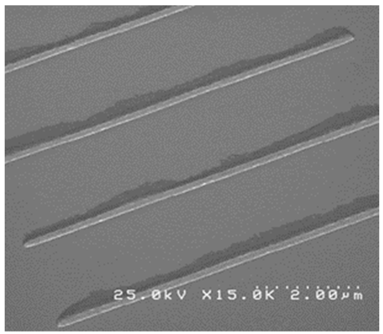
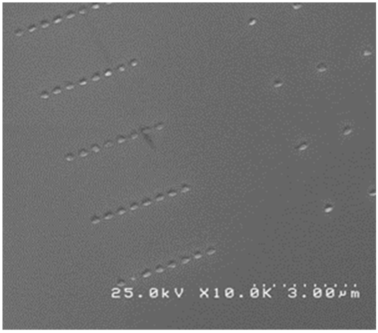
We have obtained regular shapes of circles and triangles with exposed characteristic dimensions of 200 nm and 400 nm in the case of test 1. The area of the shapes was enlarged by almost 80% with respect to the exposed area after performing reactive ion etching (test 1), but the shape of the structures remained relatively identical to the exposed shape. The best results obtained within test 1 were achieved for a current of 15 pA, with the corresponding SEM images shown in Figure 3, Figure 4 and Figure 5.
The best nanostructure engraving results obtained within test 2 were achieved for a current of 15 pA, where the aspect-to-ratio has been proven to be optimal. The corresponding SEM images are shown in Figure 6 and Figure 7.
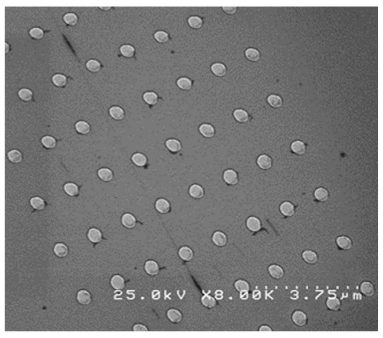
Taking into account all of the potential shapes of the nanostructures that we have shown can be successfully engineered through lithography engraving, we have chosen the regular array of FePt circles, magnetic dots, for further investigation. This choice was made considering the potential of such a nanostructure to be developed into an array of nanodevices that are individually addressable. The creation of wide area arrays of magnetic dots or nanostructures of identical rectangular shapes, regularly dispersed and integrated onto functionalized substrates with logic capabilities, would allow fabrication of complex architecture structures where the magnitude and direction of magnetic moments may be individually addressed and exploited for applications in the fields of magnetic nanosensors and molecular detection. Systems exhibiting magnetoresistive effect (GMR) materials are generally made of conductive regions, alternated with or separated by magnetic regions [18,19]. Spin reorientation in the magnetic regions, due to application of a magnetic field, causes spin dependent scattering of conduction electrons moving through the material at the conductor/magnet interface. The presence of an applied magnetic field may be easily detected by the changes in the resistivity of the material, this being the main effect used in applications such as magnetoresistive sensors and biosensors. The magnetoresistive materials may be used as magnetic biosensors via detection of the smallest changes in the magnetic field that are able to cause resistance change.
3.2. Structural Analysis of the Regular Arrays of Magnetic Structures
The regular arrays of magnetic dots, periodically dispersed, are imaged in Figure 7 and were structurally investigated by means of X-ray diffraction in a grazing incidence geometry. Such a grazing geometry of X-ray beam incidence was carefully chosen, with an angle of 0.8 up to 1.5 degrees, in such a manner as to minimize the effect and influence of the substrate contribution into the overall patterns. The diffractograms were recorded between 20 and 95 degrees in 2 theta. For improved clarity of the structure of the regular arrays, the diffractogram of the pristine substrate in the absence of the engraved regular arrays was also recorded and was subsequently subtracted from the diffractogram of the engraved structure, the difference being subsequently normalized for improved clarity. We thus obtained a clear X-ray spectrum, consisting of diffracted beams originating only from the regular array of FePt circles. It is known that, usually, the bulk FePt binary alloy, either equiatomic or off-stoichiometric, is formed in a disordered A1-type cubic structure and, upon annealing, undergoes a structural disorder–order phase transformation. Following such transformation, the FePt exhibits the ordered, tetragonal L10 FePt phase, which is the phase structure responsible for the hard magnetic properties of the system.
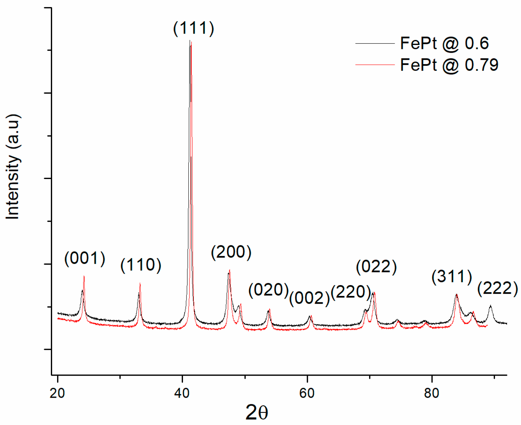
In Figure 8, which depicts the XRD patterns corresponding to the samples exposed at 0.6 μC/cm2 and at 0.79 μC/cm2 all the main Bragg lines of tetragonal L10 FePt are present in both samples. There is a strong presence of the superlattice peaks, (001) and (110) diffraction lines, as well as the presence of main (111) Bragg lines followed by other superlattice peaks, distinctly split (200) fundamental reflection, recorded at around 48–49 degrees in 2 theta. It should be mentioned that the two main superlattice peaks of tetragonal L10, the (001) and (110) reflections occur for the employed Cu Kα radiation at about 23° and 32°, respectively. It should also be mentioned that the six main Bragg lines of the tetragonal FePt, from lower to higher angles, are, in order, attributed to (001), (110), (111), (200), (020), (002), (220), (022), (311) and (222) hkl planes reflections. The peak assignation has been undertaken in agreement with the ICDD card 03-065-9121. Beyond the occurrence of the superlattice peaks (001) and (110), another distinct signature of the occurrence of the tetragonal L10 phase is the fact that the (200), (220) and (311) peaks are split into two. Such a feature has been encountered in other works on FePt [20,21,22] and has been unambiguously regarded as a further proof of the occurrence of the L10 phase, this being due to the tetragonally distorted planes and giving rise to the spectral splitting observed in these peaks. Upon the fitting of the XRD spectra, we have also derived the average crystallographic grain size of the L10 FePt. It has been thus observed that the average grain size of the tetragonal L10 phase ranges from 20 to 24 nm on increasing the exposure dose. We conclude that in these XRD results, only the L10 phase has been identified. In relation to the previous studies [8,9], where it has been shown that not all of the FePt dots were transformed from a cubic A1 to tetragonal L10 structure, which was detrimental to the magnetic anisotropy, in our case all of the observed dots seem to be in their ordered L10 tetragonal crystal structure.
3.3. High-Resolution Transmission Electron Microscopy and Electron Diffraction Results
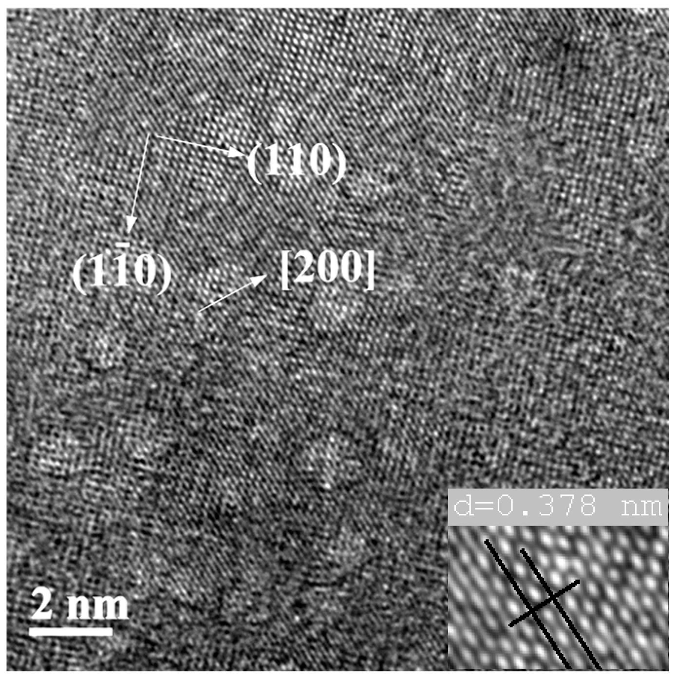
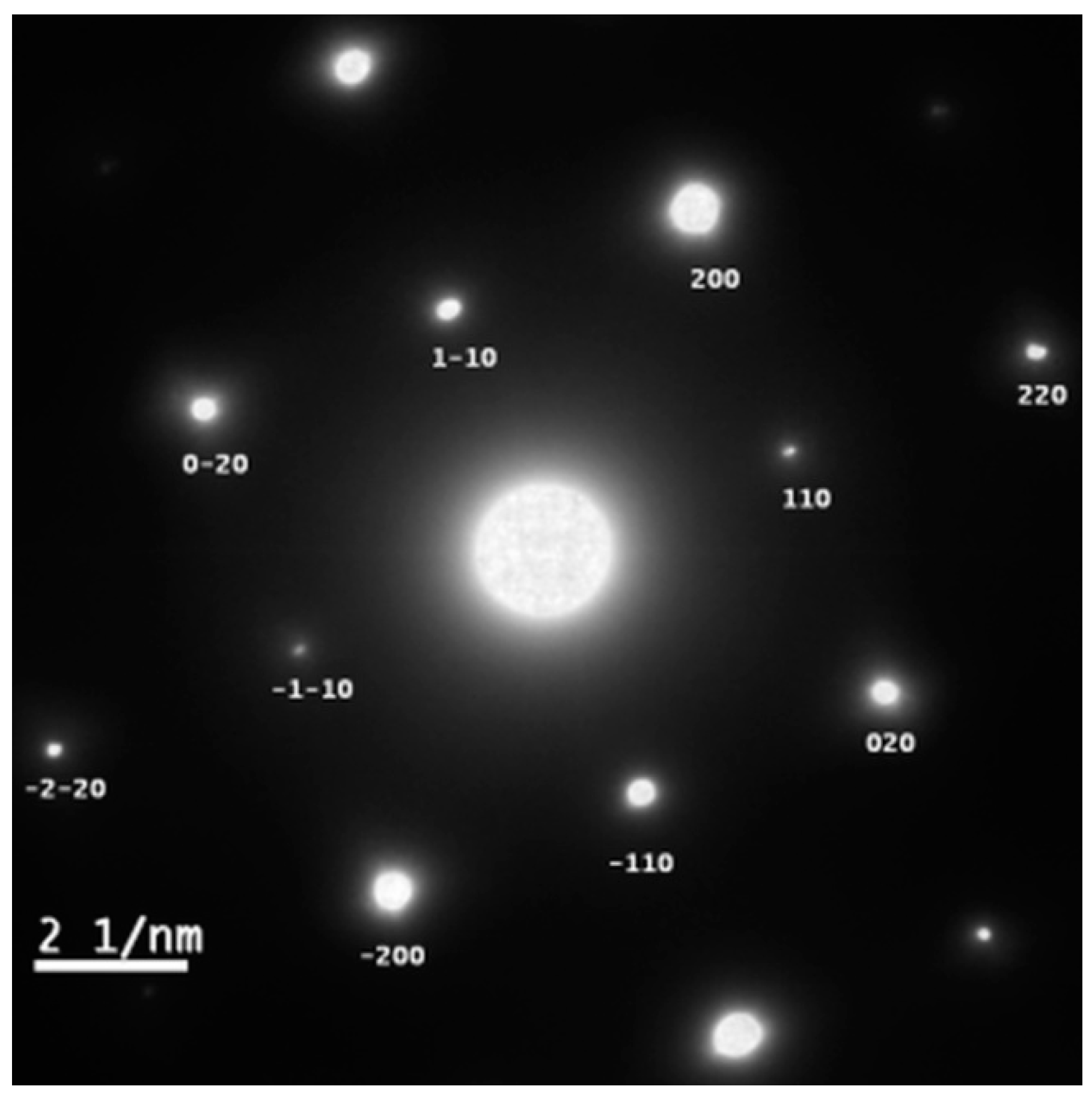
The microstructure of the granular regions on the magnetic dot surfaces, on the sample with circular shapes shown in Figure 7, was imaged with the help of the transmission electron microscopy in the high-resolution mode, coupled with the observation of the electron diffraction patterns, within the imaged areas on the dots surface. In the imaging area the sample was thinned down by ion etching of the substrate with the focused ion beam module of the microscope. A typical magnified image obtained in HRTEM is shown in Figure 9. The high-resolution image, recorded in phase contrast imaging mode, reveals small nanocrystals of ordered tetragonal L10 FePt symmetry. The observed microstructure is apparently made of ordered FePt crystallites, with a size of between approximately 4 and 8 nm, and which are distributed within a wide area between 13 and 18 nm. The reticular interplanar distances, clearly observed and measured on the image, prove the occurrence of the (110) and (1–10) superlattice reflections, which are indeed typical for the tetragonal L10 FePt phase. This confirms, in a more illustrative way, the findings obtained from XRD analysis, detailed above. Another main Bragg reflection of the L10 phase, the (200) reflection is also observed and accurately measured on the image through the measuring of the interplanar distance. Taking into account that the limiting critical size for single-magnetic domains is 55 nm for L10 FePt nanograins [23] it can safely be concluded that the FePt regions are magnetically single domains, irrespective of their crystal symmetry or of their degree of crystallographic ordering. Figure 10 depicts the selected area electron diffraction image corresponding to the area that is imaged in real space in Figure 9. Being essentially a map of the reciprocal space, the SAED image illustrates via the brightness of the observed spots, the intensity of the corresponding planar reflection, thus indicating quantitatively the abundance of the ordered FePt grains. It can be seen that SAED analysis also confirms the occurrence of the ordered L10 FePt phase in the imaged magnetic dot. The presence of the main superlattice spots, the (001) and (110) Bragg reflections of L10 phase, in the SAED patterns, proves the occurrence of both crystallographic orientations, with the tetragonal c-axis perpendicular and parallel to the surface normal. Here, the atomic planes of a (110) nature are seen, which again confirms the occurrence of the superlattice reflections.
It is to be noted, however, that while Figure 9 is only an illustrative example, several other high-resolution images have been recorded, and nanocrystals of a tetragonal symmetry with detectable (001) planes, and with a reticular distance of d001 = 3.78 Å, are observed in many other imaged areas, not shown here, thus confirming the extended L10 ordering alongside the magnetic dot surface. It has been explained before that two crystallographic variants are retrieved, one having the c-axis in plane and the other having the c-axis in an orientation normal to the observing plane. All of the c lattice parameter values measured in the observed nanocrystals with tetragonal symmetry are in good agreement with the XRD results. In the same image, a second superlattice spot attributed to the (110) Bragg reflection is observed, with a reticular distance d110 = 1.91 Å.
All of the structural data are thus consistent with each other and unambiguously prove the formation of the highly ordered L10 FePt of tetragonal symmetry.
3.4. Magnetic Investigations of the Regular Arrays of Magnetic Nanostructures
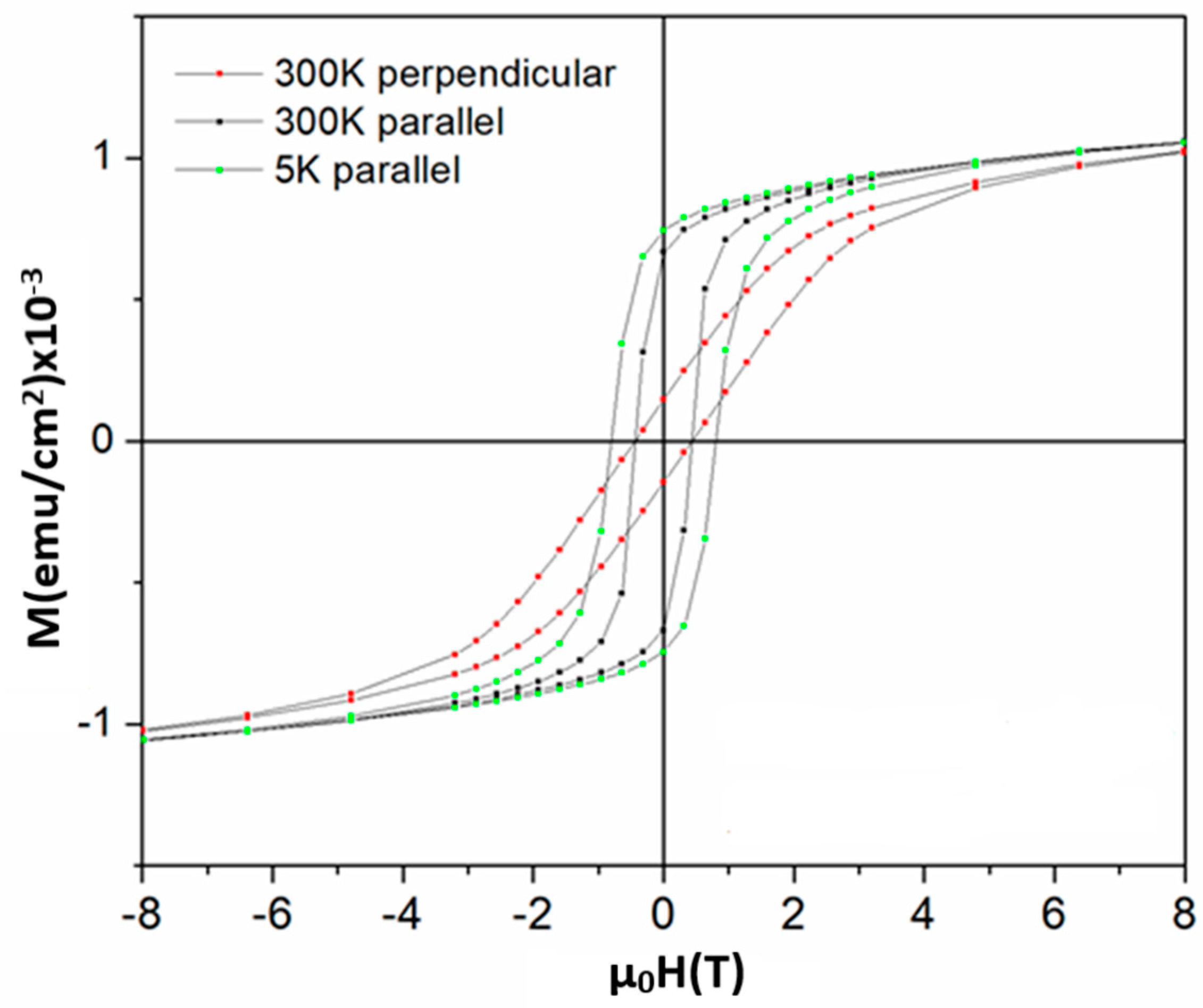
In order to assess the magnetic performances of the arrays, an investigation using the magnetic property measurement system (MPMS) was undertaken. Magnetic hysteresis loops have been measured both at 5 K and at 300 K in parallel and perpendicular orientation, in an applied field of up to 5 Tesla. Figure 11 depicts the magnetic behavior of the regular array of FePt circles, as shown in Figure 7. Because the diffraction measurements did not provide any significant differences between various exposure rates of the engraving, we have chosen to show only the sample engraved with the maximum exposure rate of 0.79 μC/cm2 as the sample engraved at 0.6 μC/cm2 had shown quite similar behavior. The magnetic hysteresis loops, recorded both in perpendicular and parallel geometry, show traits compatible with hard magnetic materials, with significant coercivity and high saturation magnetization. It has features that show the monophased magnetic character of the sample and this is in agreement with the observed microstructure, composed of hard L10 binary FePt. It is worth mentioning that, at 300 K, there are strong differences between the shape of the hysteresis loops recorded in parallel and in perpendicular geometry. The elongated shape of the loop in perpendicular geometry, as opposed to the rectangular shape in the case of the loop in parallel geometry, witnesses a pronounced in-plane magnetocrystalline anisotropy. Indeed, it has been shown that such nano-islands of FePt can exhibit a strong magnetocrystalline anisotropy of about 7 × 10⁶ J/m3 [24]. The shape of the hysteresis loops is compatible with the presence of the L10 FePt phase, exhibiting increased saturation magnetization, remanent magnetization and magnetic coercivity.
In fact, it is observed that the measured sample has magnetic coercive fields between 0.45 and 0.8 T, equivalent to 4.5 and 8 kOe, respectively, measured at 300 K and 5 K respectively. For the calculation of the magnetic coercive field, we assumed the sample geometry as being that observed in the SEM images, such as in Figure 6, with a total assumed thickness close to the nominal 70 nm. For calculation of the filling factor, we assumed a regular array, as per that in Figure 7, where the dots are of 335 nm diameter and are spaced by 1200 nm in each direction. Taking into account the size of the image and the number of dots per image we have calculated a filling factor of about 12.7%. Taken into account this factor we have thus calculated the saturation magnetization for each of the FePt dot to be about 8.82 emu/cm2. The remanent magnetization values are high, namely 5.98 emu/cm2 (5.43 emu/cm2 at 300 K), comparable to those of L10 FePt bulk alloys. The spin magnetic moment at the Fe sites is calculated from the experimental data to be µS = (2.37 ± 0.13) µB at 300 K for the sample @0.79 μC/cm2. It is important to notice that, in the investigated array of FePt circles, the microstructure consists of only the tetragonal L10 phase, and that this microstructure is well reflected in the overall magnetic behavior. The saturation magnetization is also proven to be high, which is a good prerequisite for obtaining an elevated maximum energy product which is the Figure of Merit for any nanomagnetic structure, albeit nanoparticle, thin film or engraved dots and circles. These findings are encouraging, as they show potential for developing regular arrays of uniformly shaped magnetic entities with good magnetic performances in view of potential and various applications, from biomagnetic sensing through the magnetoresistance effect up to THz spintronic devices for telecom applications and heating dot magnetic recording.
4. Conclusions
A versatile method of engraving magnetic materials with various shapes, sizes and orientations using e-beam lithography has been described and shown to be potentially suitable for achieving the building blocks of further development of nanomagnet–logic structures for several types of applications, ranging from magnetoresistive biomagnetic sensors to devices for THz spintronics. As the method has been shown to be reliable when providing various regularly spaced shapes of magnetic material by varying the exposure dose during the pre-patterning, we have focused on the structural and magnetic characterization of a nanodevice consisting of regular arrays of FePt circles or dots. Structural characterization by X-ray diffraction and HRTEM has shown that the procedure provided monodomain FePt magnetic dots, where the tetragonal L10 phase is already formed, as proven by the occurrence of the superlattice peaks. Moreover, the magnetic characterization provided more insight into the potential of such arrays of magnetic devices. Hysteresis loops recorded for the array of FePt dots were consistent with the findings from XRD and provided good values of magnetic coercivity (0.8 T), remanent magnetization (5.98 emu/cm2) and saturation magnetization (8.82 emu/cm2), values that are comparable to those obtained for bulk L10 alloys. These findings are encouraging, as they show potential for developing regular arrays of uniformly shaped magnetic entities with strong magnetic performances in view of potential and various applications, from biomagnetic sensing through to magnetoresistance effect and up to THz spintronic devices for telecom applications.
Author Contributions
Conceptualization and methodology, O.C.; formal analysis and investigation, A.D.C.; writing—original draft preparation, A.D.C.; writing—review and editing, O.C. All authors have read and agreed to the published version of the manuscript.
Funding
This research was funded by Romanian Ministry of Research, Innovation and Digitalization, through IDEI grant PCE 79/2022, PN-III-P4-PCE-2021-0573 and by EU under Romanian Recovery and Resilience Plan PNRR, 236 Pillar III, Component C9-I8, contract 760085/23 May 2023.
Data Availability Statement
The data presented in this study are available on request from the corresponding author. The data are not publicly available due to foreseen patenting potential.
Conflicts of Interest
The authors declare no conflict of interest. The funders had no role in the design of the study; in the collection, analyses, or interpretation of data; in the writing of the manuscript; or in the decision to publish the results.
References
- Murray, C.B.; Norris, D.J.; Bawendi, M.G. Synthesis and characterization of nearly monodisperse CdE (E = sulfur, selenium, tellurium) semiconductor nanocrystallites. J. Amer. Chem. Soc. 1993, 115, 8706–8715. [Google Scholar] [CrossRef]
- Liu, W.Q.; Wong, P.K.L.; Xu, Y.B. Hybrid spintronic materials: Growth, structure and properties. Prog. Mater. Sci. 2019, 99, 27–105. [Google Scholar] [CrossRef]
- Vedmedenko, E.Y.; Kawakami, R.K.; Sheka, D.D.; Gambardella, P.; Kirilyuk, A.; Hirohata, A.; Binek, C.; Chubykalo-Fesenko, O.; Sanvito, S.; Kirby, B.J.; et al. The 2020 magnetism roadmap. J. Phys. D Appl. Phys. 2020, 53, 453001. [Google Scholar] [CrossRef]
- Mohan, J.R.; Medwal, R.; Gupta, S.; Gogia, K.; Vas, J.V.; Gupta, R.; Deka, A.; Rawat, R.S.; Subramanian, A.; Fukuma, Y. Nonstoichiometric FePt Nanoclusters for Heated Dot Magnetic Recording Media. ACS Appl. Nano Mater. 2021, 4, 7079–7085. [Google Scholar] [CrossRef]
- Medwal, R.; Gautam, S.; Gupta, S.; Chae, K.H.; Asokan, K.; Deen, G.R.; Rawat, R.S.; Katiyar, R.S.; Annapoorni, S. Self-Stabilized Carbon-L10 FePt Nanoparticles for Heated Dot Recording Media. IEEE Magn. Lett. 2018, 9, 5504105. [Google Scholar] [CrossRef]
- Kuo, D.S.; Lee, K.Y.; Yang, X.M.; Xiao, S.G.; Hsu, Y.; Yu, Z.; Feldbaum, M.; Klemmer, T.; Kubota, Y.; Thiele, J.-U.; et al. Heated Dot Magnetic Recording Media—Path to 10 TDOTS/in2. In Proceedings of the 2016 International Conference of Asian Union of Magnetics Societies (ICAUMS), Tainan, Taiwan, 1–5 August 2016; p. 1. [Google Scholar]
- Hai, L. Storage Physics and Noise Mechanism in Heat-Assisted Magnetic Recording. Ph.D. Thesis, Carnegie Mellon University, Pittsburgh, PA, USA, 2016. [Google Scholar]
- Yan, Z.J.; Takahashi, S.; Hasegawa, T.; Ishio, S.; Kondo, Y.; Ariake, J. Towards an understanding of microstructure of patterned FePt dots by magnetometry using pulse fields. J. Magn. Magn. Mater. 2014, 349, 5–8. [Google Scholar] [CrossRef]
- Yan, Z.J.; Takahashi, S.; Hasegawa, T.; Ishio, S.; Kondo, Y.; Ariake, J.; Xue, D.S. Understanding magnetic properties of arrays of small FePt dots with perpendicular anisotropy. J. Magn. Magn. Mater. 2012, 324, 3737–3740. [Google Scholar] [CrossRef]
- Li, G.X.; Sun, S.H.; Wilson, R.J.; White, R.L.; Pourmand, N.; Wang, S.X. Spin valve sensors for ultrasensitive detection of superparamagnetic nanoparticles for biological applications. Sens. Actuators A Phys. 2006, 126, 98–106. [Google Scholar] [CrossRef]
- Stanciu, C.D.; Hansteen, F.; Kimel, A.V.; Kirilyuk, A.; Tsukamoto, A.; Itoh, A.; Rasing, T. All-Optical Magnetic Recording with Circularly Polarized Light. Phys. Rev. Lett. 2007, 99, 047601. [Google Scholar] [CrossRef]
- Radu, I.; Vahaplar, K.; Stamm, C.; Kachel, T.; Pontius, N.; Dürr, H.A.; Ostler, T.A.; Barker, J.; Evans, R.F.L.; Chantrell, R.W.; et al. Transient ferromagnetic-like state mediating ultrafast reversal of antiferromagnetically coupled spins. Nature 2011, 472, 205. [Google Scholar] [CrossRef]
- Mangin, S.; Gottwald, M.; Lambert, C.H.; Steil, D.; Uhlíř, V.; Pang, L.; Hehn, M.; Alebrand, S.; Cinchetti, M.; Malinowski, G.; et al. Engineered materials for all-optical helicity-dependent magnetic switching. Nat. Mater. 2014, 13, 286–292. [Google Scholar] [CrossRef]
- Li, T.; Patz, A.; Mouchliadis, L.; Yan, J.Q.; Lograsso, T.A.; Perakis, I.E.; Wang, J.G. Femtosecond switching of magnetism via strongly correlated spin–charge quantum excitations. Nature 2013, 496, 69–73. [Google Scholar] [CrossRef]
- Chen, Y.; Wang, X.; Sun, Z.; Li, H. The application of spintronic devices in magnetic bio-sensing. In Proceedings of the 2nd Asia Symposium on Quality Electronic Design (ASQED), Penang, Malaysia, 3–4 August 2010; pp. 230–234. [Google Scholar] [CrossRef]
- Su, D.Q.; Wu, K.; Saha, R.; Peng, C.Y.; Wang, J.P. Advances in Magnetoresistive Biosensors. Micromachines 2020, 11, 34. [Google Scholar] [CrossRef]
- Dey, C.; Yari, P.; Wu, K. Recent advances in magnetoresistance biosensors: A short review. Nano Futures 2023, 7, 012002. [Google Scholar] [CrossRef]
- Crisan, A.D.; Vasiliu, F.; Nicula, R.; Bartha, C.; Mercioniu, I.; Crisan, O. Thermodynamic, structural and magnetic studies of phase transformations in MnAl nanocomposite alloys. Mater. Charact. 2018, 140, 1–8. [Google Scholar] [CrossRef]
- Crisan, A.D.; Crisan, O.; Randrianantoandro, N.; Valeanu, M.; Morariu, M.; Burkel, E. Crystallization processes in Fe-Pt-Nb-B melt spun ribbons. Mater. Sci. Eng. C-Biomim. Supramolec. Syst. 2007, 27, 1283–1285. [Google Scholar] [CrossRef]
- Hong, Y.; de Moraes, I.; Eslava, G.G.; Grenier, S.; Bellet-Amalric, E.; Dias, A.; Bonfim, M.; Ranno, L.; Devillers, T.; Dempsey, N.M. A high throughput study of both compositionally graded and homogeneous Fe-Pt thin films. J. Mater. Res. Technol. 2022, 18, 1245–1255. [Google Scholar] [CrossRef]
- Yu, J.; Xiao, T.; Wang, X.; Zhou, X.; Wang, X.; Peng, L.; Zhao, Y.; Wang, J.; Chen, J.; Yin, H.; et al. A Controllability Investigation of Magnetic Properties for FePt Alloy Nanocomposite Thin Films. Nanomaterials 2019, 9, 53. [Google Scholar] [CrossRef]
- Xie, Z.; Cai, Y.; Tang, M.; Zhou, J.; Liu, J.; Peng, J.; Jiang, T.; Shi, Z.; Chen, Z. Fluence and Temperature Dependences of Laser-Induced Ultrafast Demagnetization and Recovery Dynamics in L10-FePt Thin Film. Materials 2023, 16, 5086. [Google Scholar] [CrossRef]
- Kikuchi, N.; Okamoto, S.; Kitakami, O. The critical size between single domain and multidomain in L10-FePt. J. Appl. Phys. 2008, 103, 07D511. [Google Scholar] [CrossRef]
- Sun, S. Recent Advances in Chemical Synthesis, Self-Assembly, and Applications of FePt Nanoparticles. Adv. Mater. 2006, 18, 393–403. [Google Scholar] [CrossRef]
Figure 1.
The schematics of the L10 tetragonal unit cell of FePt. Fe atoms are figured in red and Pt atoms in grey.
Figure 1.
The schematics of the L10 tetragonal unit cell of FePt. Fe atoms are figured in red and Pt atoms in grey.

Figure 2.
SEM image of wires with exposed thickness of 200 nm, obtained at different doses ranging from 0.6 μC/cm2 (up) to 0.79 μC/cm2 (down). The ruler at bottom right represents the overall scale of the image.
Figure 2.
SEM image of wires with exposed thickness of 200 nm, obtained at different doses ranging from 0.6 μC/cm2 (up) to 0.79 μC/cm2 (down). The ruler at bottom right represents the overall scale of the image.

Figure 3.
Wires with exposed thickness of 100 nm, each one corresponding to a dose in the interval 0.76–0.79 μC/cm2 in descending order from top to bottom.
Figure 3.
Wires with exposed thickness of 100 nm, each one corresponding to a dose in the interval 0.76–0.79 μC/cm2 in descending order from top to bottom.

Figure 4.
FePt circles with exposed diameters of 335 nm and the same circles overlapped over a distance of 200 nm on the y direction—corresponding to a dose in the interval 0.76–0.79 μC/cm2—in descending order from top to bottom. In the image, the structures to the left are circles with exposed diameters of 200 nm spaced at a distance of 200 nm, while the structures on the right are circles with an exposed diameter of 200 nm spaced at a distance of 1200 nm.

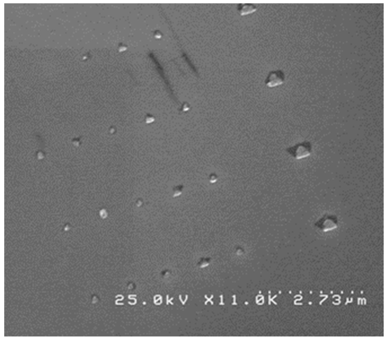
Figure 5.
Equilateral FePt triangles with exposed characteristic dimensions of 200 nm spaced at a distance of 1200 nm—corresponding to a dose in the interval 0.76–0.79 μC/cm2—in descending order from top to bottom, on the left of the image. Equilateral triangles with exposed characteristic dimensions of 400 nm spaced at a distance of 1200 nm—corresponding to a dose in the interval 0.76–0.79 μC/cm2—in descending order from top to bottom, on the right of the image.

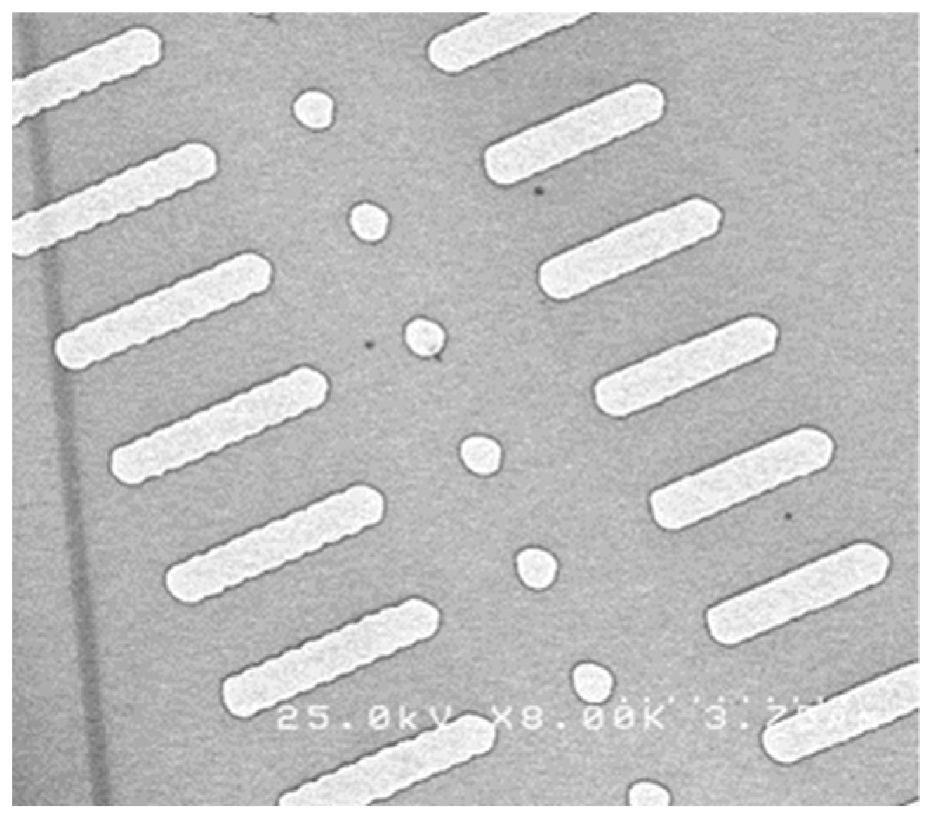
Figure 6.
Tangent FePt circles with exposed diameters of 335 nm, overlapped over 200 nm (column of structures on the left and on the right of the image); circles with exposed diameters of 335 nm (central column); the corresponding doses are in the range of 0.66–0.71 μC/cm2 in ascending order from top of the image to the bottom.

Figure 7.
Regular array of FePt circles, magnetic dots, 335 nm in size, spaced at about 1200 nm in both x and y directions. The magnetic dots height, or their thickness, are dictated and finely tuned by the exposure dose.
Figure 7.
Regular array of FePt circles, magnetic dots, 335 nm in size, spaced at about 1200 nm in both x and y directions. The magnetic dots height, or their thickness, are dictated and finely tuned by the exposure dose.

Figure 8.
X-ray diffractograms for two of the regular arrays of FePt circles, engraved with an exposure dose of 0.6 and 0.79 μC/cm2, respectively.
Figure 8.
X-ray diffractograms for two of the regular arrays of FePt circles, engraved with an exposure dose of 0.6 and 0.79 μC/cm2, respectively.

Figure 9.
HRTEM image of an FePt magnetic dot. Atomic planes are identified, and reticular distances allow identification of superlattice peaks of L10 FePt.
Figure 9.
HRTEM image of an FePt magnetic dot. Atomic planes are identified, and reticular distances allow identification of superlattice peaks of L10 FePt.

Figure 10.
A representative SAED pattern. In the reciprocal space, the superlattice reflections (110), (020) and (220) are also observed.
Figure 10.
A representative SAED pattern. In the reciprocal space, the superlattice reflections (110), (020) and (220) are also observed.

Figure 11.
The 300 K and 5 K hysteresis loops of the regular arrays of FePt circles, as seen in Figure 7, recorded in perpendicular and parallel applied magnetic field, with respect to the array plane. The loops correspond to the sample engraved with the maximum exposure rate of 0.79 μC/cm2.
Figure 11.
The 300 K and 5 K hysteresis loops of the regular arrays of FePt circles, as seen in Figure 7, recorded in perpendicular and parallel applied magnetic field, with respect to the array plane. The loops correspond to the sample engraved with the maximum exposure rate of 0.79 μC/cm2.

Disclaimer/Publisher’s Note: The statements, opinions and data contained in all publications are solely those of the individual author(s) and contributor(s) and not of MDPI and/or the editor(s). MDPI and/or the editor(s) disclaim responsibility for any injury to people or property resulting from any ideas, methods, instructions or products referred to in the content. |
© 2023 by the authors. Licensee MDPI, Basel, Switzerland. This article is an open access article distributed under the terms and conditions of the Creative Commons Attribution (CC BY) license (https://creativecommons.org/licenses/by/4.0/).
Share and Cite
MDPI and ACS Style
Crisan, O.; Crisan, A.D. Lithographically Ordered FePt L10 Dots with High Coercivity for Logic-Conditioned Magnetic Nanostructures. Crystals 2024, 14, 58. https://doi.org/10.3390/cryst14010058
AMA Style
Crisan O, Crisan AD. Lithographically Ordered FePt L10 Dots with High Coercivity for Logic-Conditioned Magnetic Nanostructures. Crystals. 2024; 14(1):58. https://doi.org/10.3390/cryst14010058
Chicago/Turabian StyleCrisan, Ovidiu, and Alina Daniela Crisan. 2024. "Lithographically Ordered FePt L10 Dots with High Coercivity for Logic-Conditioned Magnetic Nanostructures" Crystals 14, no. 1: 58. https://doi.org/10.3390/cryst14010058
Note that from the first issue of 2016, this journal uses article numbers instead of page numbers. See further details here.