Article

Toward Reliable Compact Modeling of Multilevel 1T-1R RRAM Devices for Neuromorphic Systems

by
Emilio Pérez-Bosch Quesada
1,*,
Rocío Romero-Zaliz
2,
Eduardo Pérez
1,
Mamathamba Kalishettyhalli Mahadevaiah
1,
John Reuben
3,
Markus Andreas Schubert
1,
Francisco Jiménez-Molinos
4,
Juan Bautista Roldán
4 and
Christian Wenger
1,5
1
IHP-Leibniz-Institut für Innovative Mikroelektronik, 15230 Frankfurt, Germany
2
Andalusian Research Institute on Data Science and Computational Intelligence, University of Granada, 18071 Granada, Spain
3
Computer Science 3—Computer Architecture, Friedrich-Alexander-Universität (FAU) Erlangen-Nürnberg, 91058 Erlangen, Germany
4
Department of Electronics and Computer Technology, University of Granada, 18071 Granada, Spain
5
BTU Cottbus-Senftenberg, 01968 Cottbus, Germany
*
Author to whom correspondence should be addressed.
Electronics 2021, 10(6), 645; https://doi.org/10.3390/electronics10060645
Submission received: 23 February 2021 / Revised: 5 March 2021 / Accepted: 7 March 2021 / Published: 11 March 2021
(This article belongs to the Special Issue Memristive Devices and Systems: Modelling, Properties & Applications)

Abstract

:
In this work, three different RRAM compact models implemented in Verilog-A are analyzed and evaluated in order to reproduce the multilevel approach based on the switching capability of experimental devices. These models are integrated in 1T-1R cells to control their analog behavior by means of the compliance current imposed by the NMOS select transistor. Four different resistance levels are simulated and assessed with experimental verification to account for their multilevel capability. Further, an Artificial Neural Network study is carried out to evaluate in a real scenario the viability of the multilevel approach under study.

1. Introduction

Considering the successful development of software-implemented Artificial Neural Networks (ANN) and their increasing integration in the commercial market, it is of special interest to consider the subsequent drawbacks that the performance of these kind of neuro-inspired networks entails. The gap between the off-chip memory units and the processing units is a clear example of one of the main shortcomings that the von Neuman architectures present. Owing to this fact, for instance, the downscaling of the electronic devices and the implementation of learning algorithms for mobile applications could be compromised. Among others, the reduction of the overall energy consumption and computation time within these networks are key aspects that the artificial intelligence research community has had in its scope for several years now [1]. As an alternative, the hardware-based neuromorphic networks have shown to be the precursor elements to step up onto a new stage in the integration of biological-inspired systems. Particularly, the RRAM technology has been taken into consideration, not only because of its integration as CMOS-compatible non-volatile memory (NVM) arrays but also because of its synaptic-like analog properties [2,3,4,5,6,7].
The implementation of RRAM cells as synaptic unions between artificial neurons allows the possibility to design and carry out ANNs featured by low-power consumption and low integration area [8]. This is possible due to the multilevel approach also known as Multi-Level Cell (MLC) behavior, consisting of modulating in multiple states the resistance/conductance of the dielectric layer in the RRAM cell. To obtain the mentioned MLC behavior, different programming techniques have been reported lately, such as gradual Reset process by consecutive identical pulses [9], applying positive and negative voltage sweeps with different stop values during the Set and Reset operations [10,11,12], modifying the compliance current imposed to the cell during the Set transition [13,14,15] and implementing multilevel incremental step pulses with verify algorithm (M-ISPVA) [16,17], among others.
Nevertheless, the existence of a gap between the device and circuit/system levels challenges the implementation of hardware-based ANN, thus the development of accurate and time-efficient RRAM models for circuit design simulations is an issue that must be tackled.
Several RRAM compact models have been developed and reviewed throughout the history of the memristor [18,19,20,21,22,23] also in the MLC approach [24]. Regarding the switching behavior of the RRAM devices, different phenomena and equations govern the implementation of each reported model and therefore, they account for different computational cost, yield and accuracy.
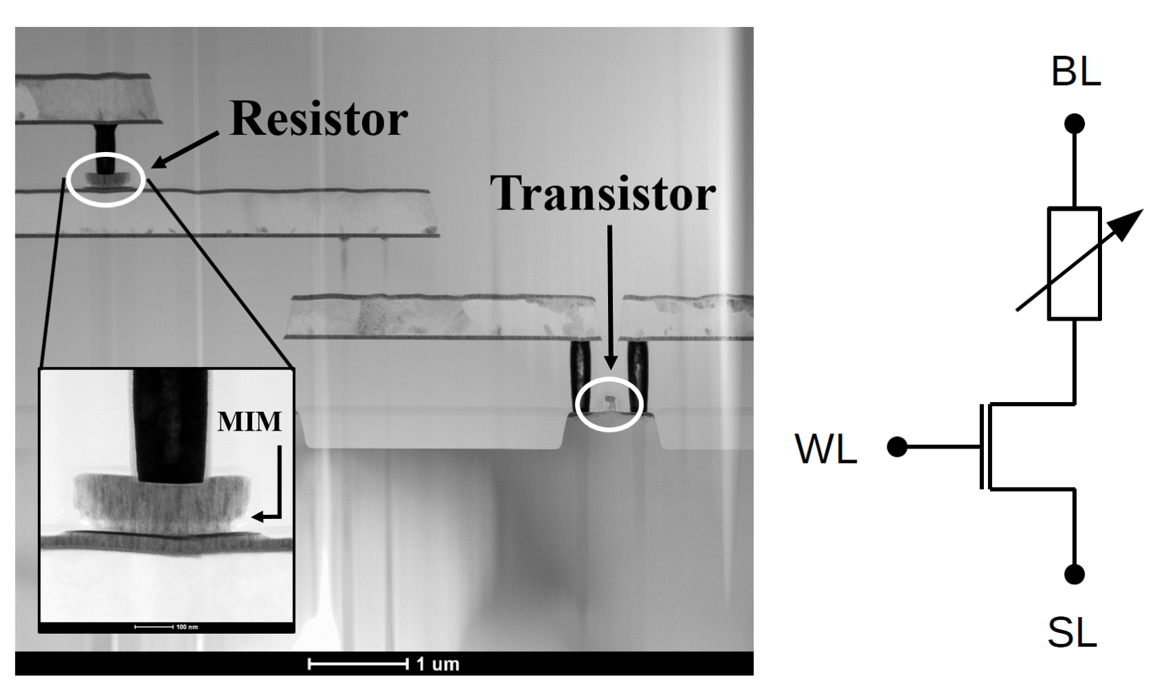
This work is focused on modeling the MLC by using the change in the compliance current in order to switch the RRAM device between various low resistance states (LRS) and a single high resistance state (HRS). This is accomplished by connecting a NMOS select transistor in series with the memristor, constituting the so called one-transistor-one-resistor (1T-1R) structure [17]. Furthermore, three different compact models implemented in Verilog-A are integrated in the mentioned 1T-1R structure to give insight into their viability in the multilevel approach. First of all, the Stanford-PKU model [25] including the modification provided by Reuben et al. for multilevel operation [26] is taken into account. Based on similar physical aspects, the Valence Change Memory model with Cylindrical shaped Filament (UGR-VCMCF) and Valence Change Memory model with Truncated-Cone shaped Filament (UGR-VCMTCF) developed by Gonzalez-Cordero et al. [27] are analyzed as well. For other modeling approaches, a revision paper was published recently [28], where the different memristor models were compared and described in depth. The experimental verification is driven by the RRAM devices fabricated using the 130 nm CMOS technology of IHP.
The abovementioned compact models are briefly detailed in Section 2, while the experimental samples characteristics are described in Section 3. The experimental verification and the subsequent modeling results are presented and discussed within Section 4. Later, an ANN study to assess the presented multilevel approach is described in Section 5. Finally, a set of conclusions are drawn in Section 6.

2. Compact Models Description

In this section, the implementation of three compact models extracted from [25,26,27] is presented. As it is indicated below, the behavior of the mentioned compact models is based on the increase and decrease of the gap distance between the tip of the conductive filament (CF) and the bottom electrode (BE). Although these compact models are based on similar physical phenomena, they consider different CF geometries, as it can be appreciated in Figure 1 and, thus, different results concerning the MLC behavior can be obtained.

2.1. Stanford-PKU Model Extended with Multilevel Capability

This model is based on the growth and disruption of a CF when an appropriate electric field is generated in the dielectric layer of the RRAM cell. This phenomenon is described by the increase or decrease of the gap distance between the CF tip and the bottom electrode within the dielectric layer (see Figure 1a) when a Reset or a Set operation take place, respectively. The gap evolution is modeled as follows:
d g d t = ν 0 e E a k b T s i n h γ a 0 q V t o x k b T ,
where g stands for the gap distance between the CF and the bottom electrode, ν 0 is a fitting parameter that accounts for the velocity dependent on the attempt-to-escape frequency, E a is the effective activation energy for vacancy generation, k b is the Boltzmann constant, a 0 is the atom spacing, q is the electron charge, V is the voltage applied to the device, t o x is the dielectric thickness and T is the device temperature, which is computed as follows:
T = T 0 + V · I · R t h ,
where T 0 is the room temperature, I is the current through the device and R t h accounts for its thermal resistance.
The variable γ is the field local enhancement factor that accounts for the material polarizability [29], which depends on the current gap distance g. The latest is bounded between g m i n and g m a x , which are the minimum and maximum possible values that this variable can have.
Finally, the total current flowing through the cell is computed as
I = I 0 · e g g 0 · s i n h V V 0 ,
where I 0 , g 0 and V 0 are fitting coefficients.
Considering the standard Stanford-PKU model [25], we observed that the MLC behavior can be accomplished by imposing different compliance currents through the cell during the Set operation, allowing the CF to grow accordingly to the electric field within the insulator layer of the MIM stack. Thus, the gap boundaries are constant during the whole simulation time. However, regarding the proposed modification by Reuben et al. [26], the minimum gap distance ( g m i n ) turns into a variable. Owing to the fact that this model modification was implemented to be integrated within a 1T-1R structure, this variable depends on the voltage applied to the gate terminal of the transistor ( V g a t e ). In this way, the NMOS transistor is assumed to be operating in the triode region and thus, it behaves as a linear resistor. Taking into account these statements, g m i n is computed as follows:
g m i n = K t h · ( W / L ) V g a t e + C ,
where K t h and C are fitting constants for a particular 1T-1R cell, which are computed taking into account the experimental multilevel measurements. W / L accounts for the aspect ratio of the NMOS transistor. It has to be considered that an extra input terminal is added to this model modification to feed the gate voltage of the NMOS transistor into its algorithm, as it can be appreciated in (4).
Thereof, in this modeling approach the minimum gap distance variable determines the LRS level of the cell depending on V g a t e . That is to say, the multilevel behavior of the RRAM model is fully controlled by limiting the CF growth and thus, the minimum gap distance between the filament and the bottom electrode.

2.2. Valence Change Memory Model with Cylindrical Shaped Filament (UGR-VCMCF)

This model accounts for the same physical phenomena presented in the standard Stanford-PKU model, in which the gap distance between the CF and the opposite electrode determines the current flow through the cell as indicated in (3). However, the CF is modeled following a cylindrical geometry (see Figure 1b) and thus, its ohmic and thermal properties are conditioned to the mentioned structure.
A more accurate thermal description is performed by using a unidimensional version of the heat equation. In particular, for a cylindrical CF, the maximum temperature along its y axis can be solved as indicated in [30]:
T = T 0 + σ e q · ξ 2 · r C F · ( e α 1 ) 2 2 · h · ( e 2 · α + 1 ) ,
where σ e q stands for the CF conductivity, computed considering the CF radius r C F and the cell radius r c e l l (see Figure 1b). ξ is the average electric field in the CF and h represents the heat transfer coefficient that accounts for the lateral heat dissipation from the CF to the dielectric. Owing to the fact that the shape of the CF is assumed to be cylindrical in this model, r C F is constant. This solution is assumed as the CF temperature T used to compute the gap evolution in (1). During the Reset operation, E a is substituted by the parameter E m (migration energy). The parameter α is calculated as follows:
α = t o x 2 2 · h k t h · r C F ,
where k t h accounts for the thermal conductivity of the CF.
Concerning the multilevel approach, unlike the modification of the Stanford-PKU model proposed by Reuben et al. presented in Section 2.1, the variation of the minimum gap distance that allows the existence of multiple LRS levels is obtained following the standard Stanford-PKU behavior, i.e., without imposing variable limits to the filament growth. Thus, the increment and decrease of the gap distance between the CF and the bottom electrode for the different conductive levels is fully accomplished by means of the compliance current imposed by the transistor integrated in the 1T-1R cell.

2.3. Valence Change Memory Model with Truncated-Cone Shaped Filament (UGR-VCMTCF)

This model considers the CF as a truncated cone and therefore, its radius is not constant along its y axis (see Figure 1c). It is supposed that a truncated-cone shaped CF with constant conductivity is analytically analogous to a cylindrical CF with a variable conductivity along its main axis, whose equivalent radius is computed as follows:
r C F g = r C F m a x · r C F m i n ,
where r C F m a x and r C F m i n stand for the maximum and minimum radii of the truncated-cone CF.
Taking into consideration the previous assumptions, the maximum temperature obtained when solving the heat equation follows the structure indicated in (5) and (6). However, the new axis-dependent conductivity σ e q and the equivalent cylindrical radius r C F g have to be considered, allowing the electric field through the CF to be dependent on the y axis.
In a similar way, (1) and (3) can be solved once the new geometry of the CF is considered and so its equivalent ohmic and thermal properties.
It also has to be considered that this model enables the possibility to configure two different values for each of the fitting parameters I 0 , V 0 and g 0 , considering the positive or negative sense of the current through the cell. This eases the possibility to determine the behavior of the model for positive and negative voltage values individually.
Analogously to the UGR-VCMCF model, the UGR-VCMTCF model achieves the MLC behavior in the same way as the standard Stanford-PKU model does, that is to say, controlling the gap distance between the tip of the CF and the bottom electrode by means of the compliance current imposed by the NMOS transistor of the 1T-1R structure.

3. Experimental Samples Characteristics

The electrical measurements were performed on single 1T-1R RRAM structures. These structures consists of a NMOS transistor connected in series to a Metal-Insulator-Metal (MIM) cell as shown in Figure 2. The NMOS transistor acts as a current limiter. The devices are fabricated using the 130 nm technology of IHP. The MIM stack consists of TiN/Al:HfO2/Ti/TiN with TiN top and bottom electrodes of 150 nm and Ti layer of 7 nm deposited by sputtering and an Al doped (about 10%) HfO2 layer of 6 nm deposited by Atomic Layer Deposition (ALD). The MIM cells are fabricated with an area of about 0.4 μ m 2 . Additionally, all the cells are encapsulated with a SiNO layer.

4. Modeling Results and Discussion

In order to validate the capability of the three described models to reproduce the MLC by changing the compliance current, we obtained a set of experimental measurements using a single 1T-1R structure detailed in Section 3. From the modeling point of view, in order to adapt the model parameters to the experimental measurements we are focused on the DC response of the devices with respect to the mentioned MLC behavior. This behavior is featured by the transition from a single HRS to three different LRSs and vice versa by modifying the compliance current imposed by the NMOS transistor during the Set operation.
The experiments were carried out by applying positive voltage sweeps between 0 V and 1.5 V with steps of 0.05 V to the top electrode (TE) of the 1T-1R cell to perform the Set operations and negative voltage sweeps between 0 V and −1.5 V with steps of −0.05 V to perform the Reset operations. The voltage sweep rate used was 0.6 V/s. The compliance current imposed to the cell was controlled by setting the gate voltage of the NMOS transistor to different values. Thereof, four conductive levels were accomplished: three LRSs corresponding to V g a t e = 1 V, 1.2 V, 1.6 V, respectively, and one HRS in which V g a t e = 2.7 V. We chose a gate voltage of 2.7 V to reduce as much as possible the resistance of the transistor during the Reset operation, easing the transition from the LRSs to the sole HRS. In total, 10 Set–Reset cycles were accomplished for each LRS level within the same sample.
The observed experimental results present typical RRAM behaviors such as abrupt Set operations at V S e t and a gradual Reset transition whose V R e s e t value depends on the accomplished LRS level, i.e., the more conductive the LRS is, the higher the voltage amplitude required to Reset the device. Table 1 gathers the most remarkable electrical characteristics observed for each of the possible transitions between states.
Concerning the simulated results, the NMOS transistor model was provided by [31] and every RRAM compact model presented within this work is tuned in to fit the median DC characteristics of the experimental measurements. All the simulations were ran in Cadence Virtuoso Analog Design Environment (ADE) [32]. The aim of the fitting procedure is to provide with one set of parameters to each model to reproduce the MLC behavior indicated above. For this purpose, different steps were accomplished based on the methodology indicated in [25,26,27]:
First, one of the LRS levels is chosen to be the reference for the fitting procedure. In this case, the median values for LRS2 are taken as a reference to establish the initial set of parameters since it is the medium level of the LRSs under study. This first step can be accomplished following the methodology proposed in [25,26]. If the reference LRS is not the most conductive one, the minimum gap distance achieved during this first step cannot reach the atomic distance a 0 (0.25 nm). Otherwise, the multilevel approach cannot be accomplished for more conductive levels. Once the model is able to reproduce the reference LRS (in our case LRS2) and the single HRS, the rest of LRS levels are evaluated by modifying the gate voltage of the transistor during the Set operation and thus, the compliance current imposed to the cell. Further adjustments might be applied to the previous set of parameters in order to match the rest of the median curves for the different resistance levels. The fitting parameters I 0 and g 0 have special influence in the conductance difference between levels (see (3)). It is mandatory to achieve different minimum gap distances for every single LRS level to reproduce the MLC behavior due to the fact that the shorter the gap distance, the more conductive the resistance state is. Table 2 exposes the achieved gap distances for each conductive level for the three models.
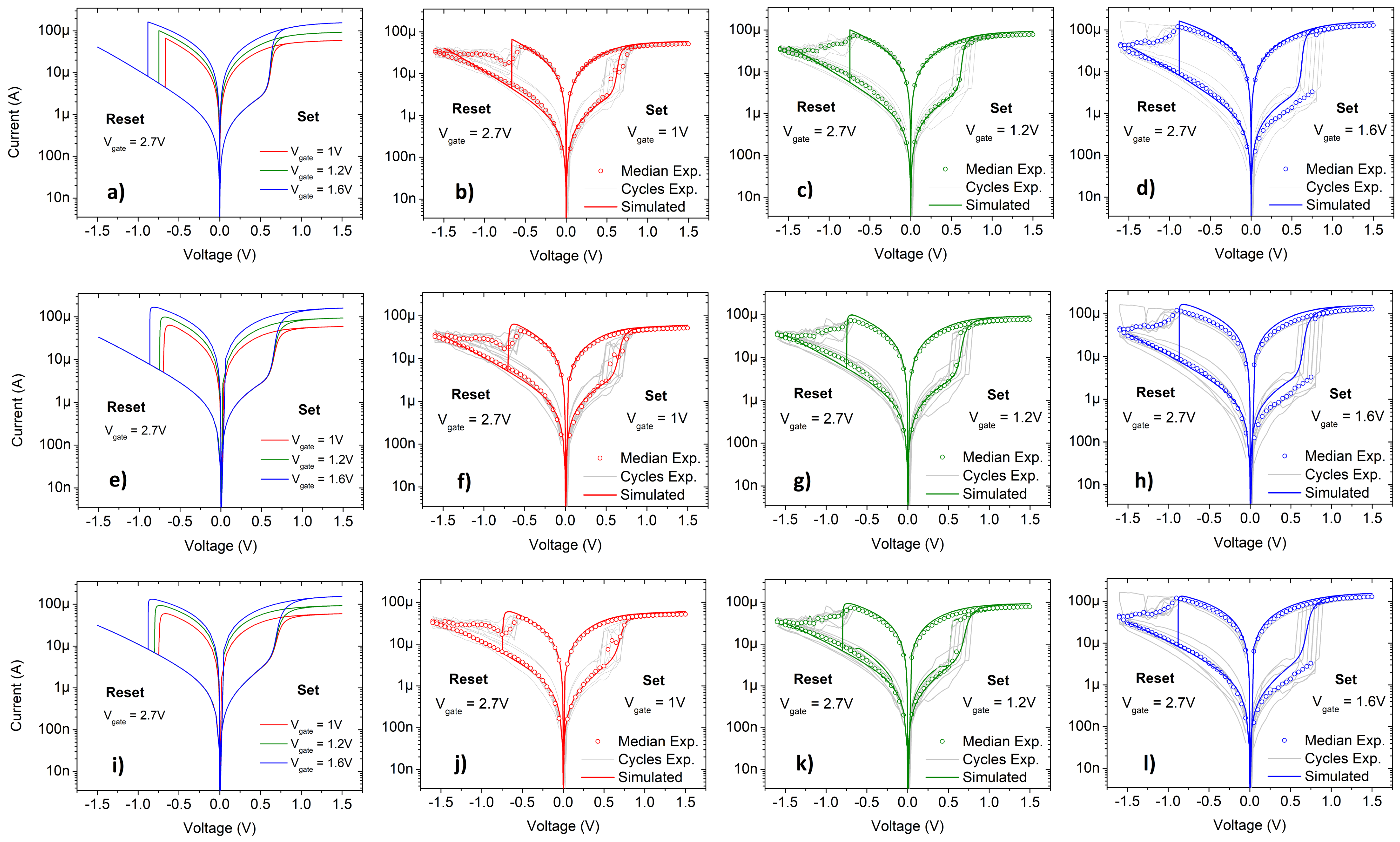
Figure 3 shows the comparison between the experimental and the simulated results extracted from the different models for each of the LRSs considered within this work. More precisely, Figure 3a–d make reference to the Stanford-PKU model extended with multilevel capability configured with the set of parameters exposed in Table 3. Figure 3e–h account for the UGR-VCMCF model fed with the parameters exposed in Table 4. Figure 3i–l make reference to the UGR-VCMTCF model configured as indicated in Table 5. All the simulations were carried out setting the HRS as the initial state ( g a p i n i = g a p m a x ) thus, a Set operation is initially performed followed by a Reset of the cell.
In general terms, despite the limited complexity of the models, the experimental results are reproduced in an acceptable way. The gap distances exposed in Table 2 match the required current levels for both, the LRSs and the sole HRS showing that this parameter is the key aspect to be considered in order to reproduce the MLC by changing the compliance current. Regarding the knee point of the Reset transition, it can be correctly simulated in all the conductive states except for LRS1 (see Figure 3b,f,j), where the maximum voltage difference for the simulated and experimental V R e s e t is up to 0.15 V. Reducing I 0 helps to minimize the mentioned voltage difference, keeping the knee point of the Reset transition in LRS2 (reference state). However, due to the linear dependence of I with respect this parameter (see (3)), this would lead to a reduction of the V R e s e t in LRS3 as well, enlarging the voltage difference between the simulated and the experimental results in this concrete point.
Due to the cycle-to-cycle variability of the experimental data measured in LRS3 (see the grey lines in Figure 3d,h,l), the HRS curve for positive voltage values presents lower median current levels as well as a higher V S e t with respect to LRS1 and LRS2. Thus, even though the simulated results fulfill the ideal behavior of LRS3, they differ from the experimental results in both mentioned aspects.
Lastly, since the memristor charge conduction is filamentary, device-to-device (D-D) variability, usually linked to technological differences in the fabrication process, is not studied. It is the cycle-to-cycle (C-C) variability during programming the factor that was considered in the experimental measurements. Modeling approaches linked to time series have been given in the literature [33,34] that can be implemented. Other modeling schemes linked to Gaussian distribution functions and Monte Carlo simulations within circuit simulators are also possible (in this case for D-D and C-C variability). The device-to-device variability that shows up during programming could be also modeled along the line described in [35], as well as the cycle-to-cycle variability. From the memory characterization point of view, retention time and endurance properties were previously studied both experimentally [16,36] and by simulation [37] from another perspective in our technology.

5. A Neural Network Study to Assess the Multilevel Approach

As it was mentioned in Section 1, the implementation of RRAM cells as synaptic unions within hardware-based ANNs is gaining momentum [2,3,4,5,6,8]. Regarding the MLC behavior taken into account in this work, it is convenient to study the performance of ANNs in this context. That implies the reduction of the precision of the synaptic weights from floating point numbers (used in conventional software-based ANNs) to a limited number of values, that is, the resistance levels defined in RRAM devices as shown in Section 4.
First, we used the SciKit-Learn [38] software tool to implement and train a Multilayer Perceptron (MLP) in order to recognize and classify handwritten digits. The selected dataset for the experiment is the well-known MNIST image dataset [39]. It is composed of 28 × 28 pixel images of 70,000 handwritten digits (labeled in the interval [ 0 , 9 ] ), divided into a training set of size 60,000 digits and a test set of size 10,000 digits. This classifier optimizes the log-loss function using stochastic gradient descent (with the back-propagation algorithm) and rectified linear unit functions (e.g., f ( x ) = x + = m a x ( 0 , x ) ) [40]. The training process was performed during 500 epochs (cycles through the full training dataset) or until the loss (or score, a prediction error of the ANN) improves by a factor of 1 × 10 4 .
We have considered different quantization strategies making use of 2, 4 and 8 levels in order to explore the accuracy of the ANN inference. In this respect, we have employed a quantization approach in line with the multilevel implementation described above for our RRAM devices (4 levels), although we also included other multilevel possibilities for the sake of completeness (2 and 8 levels). The options considered here were: Uniform-ASYMM and Uniform-SYMM, as suggested in [41]. Both methods are linear, range-based and quantify a given input data x f into x q using n bits. For instance, for n = 2 they transform the original data into 2 n = 4 levels, which is the case we have considered at the device resistance level in Section 4. Uniform-ASYMM (see (8)) is an asymmetric approach that maps the minimum and maximum of the float range to an integer range with a quantization bias term. Uniform-SYMM (see (9)) is a symmetric approach that maps the original data to the quantized range with the maximum absolute value of the minimum or maximum of the original data. In this latter case, there is no quantization bias term and it is symmetric around zero.
x q = r o u n d ( x f m i n x f ) 2 n 1 m a x x f m i n x f
x q = r o u n d x f 2 n 1 1 m a x | x f |
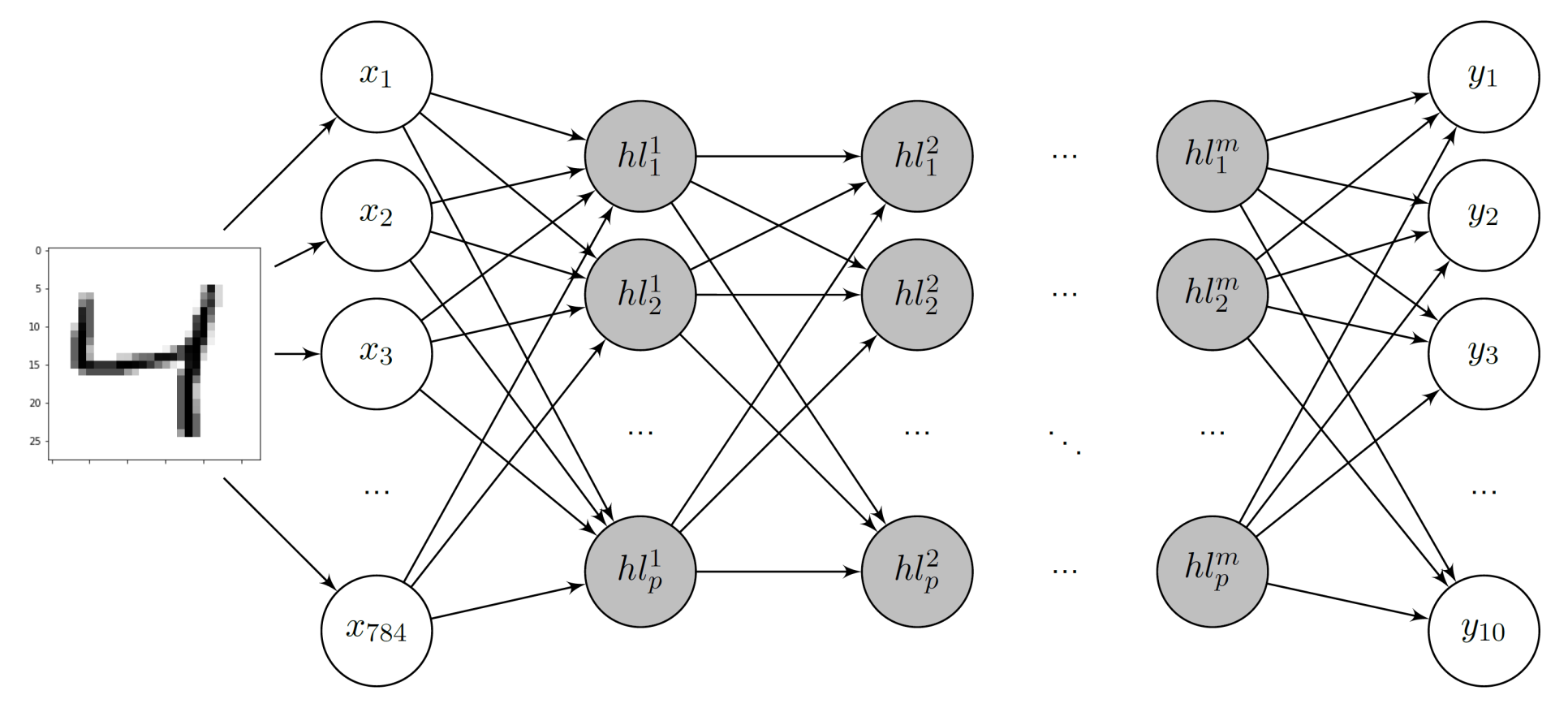
The architecture of the ANN adapted to the MNIST dataset is depicted in Figure 4. In order to simulate the usage of our ANN in a RRAM-based environment, all the synaptic weights were quantized by using the functions (8) and (9) and the number of levels (four) determined in our study, after the training process and before the final prediction on the performed tests.
The resistance levels of the memristors are connected to the use of Equations (8) and (9) for the quantization of the ANN floating point weights obtained after training. In this respect, taking into consideration that weights can be positive and negative, the implementation could be performed using two memristive devices per synapsis as demonstrated in a previous work [42].
In summary, taking into account the mentioned quantization schemes, the inference was carried out with four synaptic levels (2 bits). In total, 1, 2 and up to 3 hidden layers and 32, 64, 128, 256 and 512 perceptrons (neurons) included within each hidden layer are considered as well.
The balanced accuracies (i.e., the number of true positives divided by the total number of elements that actually belong to a class digit in our case) obtained by using the described set of parameters are shown in Table 6. The Uniform SYMM works better than the Uniform ASYMM when using four levels of quantization by an average difference of 0.13 , for all the number of hidden layers and perceptrons per layer. Nevertheless, the accuracy obtained by using the Uniform SYMM scheme with 4 levels is lower than a conventional MLP with no quantized synaptic weights by an average difference of 0.08 .
Finally, in order to assess the impact of the number of conductive levels per device on the performance of the ANN, two additional number of levels, namely, 2 (1 bit) and 8 (3 bits), were tested. Considering the implementation of RRAM devices as synaptic unions between artificial neurons, it can be assumed that these numbers of levels correspond to the number of resistance levels achieved by the basic digital behavior of the RRAM devices (two levels) and by the MLC behavior with eight resistance levels. Table 6 shows the balanced accuracies obtained with the three mentioned number of levels.
The Uniform ASYMM scheme works better than the Uniform SYMM scheme only when the number of quantizied levels is 2 by an average difference of 0.28 in the balanced accuracy. However, it seems that the Uniform ASYMM improves slower than its counterpart with the increase of the number of levels.
Both quantization methods achieve almost the same results as the original ANN (without quantization) when the number of levels increases, as it is also observed in [41]. More precisely, when the number of levels is 8, the quantized version of the ANN may obtain better results than the conventional ANN. This is due to the fact that the ANN without quantization is overfitting the training data, a common consequence observed in ANN architectures which report small training error [43]. On the contrary, due to the downgrade of the weight precision in the quantized versions, the overfitting issue is mitigated during the training period and the balanced accuracies are slightly enhanced with respect to the conventional ANN. This highlights the advantages of increasing the number of levels from 4 to 8 in the MLC behavior of the RRAM cells.
An interesting observation is the fact that by using more perceptrons in each hidden layer the balanced accuracy tends to improve in all cases, while the number of hidden layers seems to mitigate the low number of perceptrons per layer (e.g., 32 perceptrons per layer).
While investigating the coefficient (weight) distribution in each level, we discovered that not all the levels were used for quantization in the Uniform SYMM quantization scheme (data not shown). This feature could be further studied to select a lower number of levels, not in the form of 2 n , which could be useful for tryouts.
Concerning device variability, further research in the ANN context indicates that it does not affect the outcome of ANNs in the same way as in other hardware systems [44]. Due to the particular features of neural networks, in some cases, variability in the synaptic weights produces better accuracy than the ideally quantized ANN without variability. This behavior is caused by the random nature of the variability introduced, which, in some cases may shift the values of the synaptic weights closer to the optimal ANN without quantization (data not shown). Furthermore, the variability introduced in the synaptic weights may cope with a small amount of overfitting. Finally, variability do not prevent the technology from being used in a multilevel scheme in different Artificial Intelligence hardware accelerators since some prototypes have been fabricated based on these type of devices [45,46].

6. Conclusions

In this paper, three physics-based compact models for RRAMs were studied and verified with experimental data to validate their capability to simulate the multilevel behavior of the 1T-1R cells. Each of the compact models were tuned following the proposed methodology to accomplish four resistance states (2 bits) making use of a single set of parameters per model. We found out that the three models, based on similar physical phenomena, still have margin for improvement concerning the multilevel behavior of RRAM cells. However, the UGR-VCMTCF and the Stanford-PKU model extended with multilevel capability present more accurate results in terms of multilevel performance. Both the UGR-VCMCF and the UGR-VCMTCF models reproduce the MLC behavior entirely by modifying the compliance current imposed by the transistor. On the other hand, the modification of the Stanford-PKU model makes use of an extra input terminal to limit the growth of the CF. Nevertheless, it requires less parameters to reproduce the RRAM behavior. Later, a brief ANN study was performed in order to assess the MLC behavior presented in this work, showing that even with just 4 levels of quantization, the performance in classifying the MNIST database is relatively good. Finally, we also demonstrated that the next step in the accomplishment of a higher number of conductance levels in the MLC behavior can be very beneficial for the implementation of reliable ANN based on RRAM cells.

Author Contributions

Conceptualization, C.W., J.B.R. and F.J.-M.; methodology, E.P.-B.Q., J.B.R., R.R.-Z.; physical analysis of the samples, M.A.S.; writing—original draft preparation, E.P.-B.Q. and R.R.-Z.; writing—review and editing, E.P.-B.Q., R.R.-Z., E.P., M.K.M., J.R., F.J.-M., J.B.R. and C.W.; supervision, C.W., E.P., F.J.-M. and J.B.R. All authors have read and agreed to the published version of the manuscript.

Funding

The authors would like to thank the financial support by Deutsche Forschungsgemeinschaft (German Research Foundation) with Project-ID SFB1461 and by the Federal Ministry of Education and Research of Germany under grant numbers 16ES1002, 16FMD01K, 16FMD02 and 16FMD03. The authors also gratefully acknowledge the support of the Spanish Ministry of Science, Innovation and Universities and the FEDER program through project TEC2017-84321-C4-3-R and project A.TIC.117.UGR18 funded by the government of Andalusia (Spain) and the FEDER program. The publication of this article was funded by the Open Access Fund of the Leibniz Association.

Data Availability Statement

The datasets generated during and/or analysed during the current study are available from the corresponding author on reasonable request.

Conflicts of Interest

The authors declare no conflict of interest regarding the publication of this paper.

References

  1. Abiodun, O.I.; Jantan, A.; Omolara, A.E.; Dada, K.V.; Mohamed, N.A.; Arshad, H. State-of-the-art in artificial neural network applications: A survey. Heliyon 2018, 4, e00938. [Google Scholar] [CrossRef] [PubMed] [Green Version]
  2. Valentian, A.; Rummens, F.; Vianello, E.; Mesquida, T.; de Boissac, C.L.; Bichler, O.; Reita, C. Fully Integrated Spiking Neural Network with Analog Neurons and RRAM Synapses. In Proceedings of the IEEE International Electron Devices Meeting (IEDM), San Francisco, CA, USA, 7–11 December 2019; pp. 14.3.1–14.3.4. [Google Scholar]
  3. Yao, P.; Wu, H.; Gao, B.; Tang, J.; Zhang, Q.; Zhang, W.; Yang, J.J.; Qian, H. Fully hardware-implemented memristor convolutional neural network. Nature 2020, 577, 641–646. [Google Scholar] [CrossRef]
  4. Prezioso, M.; Merrikh-Bayat, F.; Hoskins, B.; Adam, G.; Likharev, K.; Strukov, D. Training and Operation of an Integrated Neuromorphic Network Based on Metal-Oxide Memristors. Nature 2014, 521. [Google Scholar] [CrossRef] [Green Version]
  5. Kang, J.F.; Gao, B.; Huang, P.; Liu, L.F.; Liu, X.Y.; Yu, H.Y.; Yu, S.; Wong, H.P. RRAM based synaptic devices for neuromorphic visual systems. In Proceedings of the IEEE International Conference on Digital Signal Processing (DSP), Singapore, 21–24 July 2015; pp. 1219–1222. [Google Scholar]
  6. Zahari, F.; Hansen, M.; Mussenbrock, T.; Ziegler, M.; Kohlstedt, H. Pattern recognition with TiOx-based memristive devices. AIMS Mater. Sci. 2015, 2, 203–216. [Google Scholar] [CrossRef]
  7. Ginnaram, S.; Qiu, J.T.; Maikap, S. Controlling Cu Migration on Resistive Switching, Artificial Synapse, and Glucose/Saliva Detection by Using an Optimized AlOx Interfacial Layer in a-COx-Based Conductive Bridge Random Access Memory. ACS Omega 2020, 5, 7032–7043. [Google Scholar] [CrossRef] [PubMed] [Green Version]
  8. Ziegler, M.; Wenger, C.; Chicca, E.; Kohlstedt, H. Tutorial: Concepts for closely mimicking biological learning with memristive devices: Principles to emulate cellular forms of learning. J. Appl. Phys. 2018, 124, 152003. [Google Scholar] [CrossRef]
  9. Huang, P.; Zhu, D.; Chen, S.; Zhou, Z.; Chen, Z.; Gao, B.; Liu, L.; Liu, X.; Kang, J. Compact Model of HfOx-Based Electronic Synaptic Devices for Neuromorphic Computing. IEEE Trans. Electron Devices 2017, 64, 614–621. [Google Scholar] [CrossRef]
  10. Maestro-Izquierdo, M.; Gonzalez, M.; Campabadal, F. Mimicking the spike-timing dependent plasticity in HfO2-based memristors at multiple time scales. Microelectron. Eng. 2019, 215, 111014. [Google Scholar] [CrossRef]
  11. Kim, W.; Menzel, S.; Wouters, D.J.; Waser, R.; Rana, V. 3-Bit Multilevel Switching by Deep Reset Phenomenon in Pt/W/TaOX/Pt-ReRAM Devices. IEEE Electron Device Lett. 2016, 37, 564–567. [Google Scholar] [CrossRef]
  12. Larentis, S.; Nardi, F.; Balatti, S.; Gilmer, D.C.; Ielmini, D. Resistive Switching by Voltage-Driven Ion Migration in Bipolar RRAM—Part II: Modeling. IEEE Trans. Electron Devices 2012, 59, 2468–2475. [Google Scholar] [CrossRef]
  13. Sedghi, N.; Li, H.; Brunell, I.; Dawson, K.; Potter, R.; Guo, Y.; Gibbon, J.; Dhanak, V.; Zhang, W.D.; Zhang, J.; et al. The role of nitrogen doping in ALD Ta2O5 and its influence on multilevel cell switching in RRAM. Appl. Phys. Lett. 2017, 110, 102902. [Google Scholar] [CrossRef] [Green Version]
  14. Misha, S.H.; Tamanna, N.; Woo, J.; Lee, S.; Song, J.; Park, J.; Lim, S.; Park, J.; Hwang, H. Effect of nitrogen doping on variability of TaOx-RRAM for low-power 3-Bit MLC applications. ECS Solid State Lett. 2015, 4, 25–28. [Google Scholar] [CrossRef] [Green Version]
  15. Prakash, A.; Deleruyelle, D.; Song, J.; Bocquet, M.; Hwang, H. Resistance controllability and variability improvement in a TaOx-based resistive memory for multilevel storage application. Appl. Phys. Lett. 2015, 106, 233104. [Google Scholar] [CrossRef] [Green Version]
  16. Pérez, E.; Zambelli, C.; Mahadevaiah, M.K.; Olivo, P.; Wenger, C. Toward Reliable Multi-Level Operation in RRAM Arrays: Improving Post-Algorithm Stability and Assessing Endurance/Data Retention. IEEE J. Electron Devices Soc. 2019, 7, 740–747. [Google Scholar] [CrossRef]
  17. Milo, V.; Zambelli, C.; Olivo, P.; Pérez, E.; Mahadevaiah, M.K.; Ossorio, O.G.; Wenger, C.; Ielmini, D. Multilevel HfO2-based RRAM devices for low-power neuromorphic networks. APL Mater. 2019, 7, 081120. [Google Scholar] [CrossRef] [Green Version]
  18. Hajri, B.; Aziza, H.; Mansour, M.M.; Chehab, A. RRAM Device Models: A Comparative Analysis With Experimental Validation. IEEE Access 2019, 7, 168963–168980. [Google Scholar] [CrossRef]
  19. Kuzum, D.; Yu, S.; Wong, H.P. Synaptic electronics: Materials, devices and applications. Nanotechnology 2013, 24, 382001. [Google Scholar] [CrossRef] [PubMed]
  20. Lekshmi Jagath, A.; Hock Leong, C.; Kumar, T.N.; Almurib, H.F. Insight into physics-based RRAM models—Review. J. Eng. 2019, 2019, 4644–4652. [Google Scholar] [CrossRef]
  21. Ielmini, D.; Milo, V. Physics-based modeling approaches of resistive switching devices for memory and in-memory computing applications. J. Comput. Electron. 2017, 16, 1121–1143. [Google Scholar] [CrossRef] [Green Version]
  22. Linn, E.; Siemon, A.; Waser, R.; Menzel, S. Applicability of Well-Established Memristive Models for Simulations of Resistive Switching Devices. IEEE Trans. Circuits Syst. Regul. Pap. 2014, 61, 2402–2410. [Google Scholar] [CrossRef] [Green Version]
  23. Menzel, S.; Siemon, A.; Ascoli, A.; Tetzlaff, R. Requirements and Challenges for Modelling Redox-based Memristive Devices. In Proceedings of the IEEE International Symposium on Circuits and Systems (ISCAS), Florence, Italy, 27–30 May 2018; pp. 1–5. [Google Scholar]
  24. Li, H.; Jiang, Z.; Huang, P.; Wu, Y.; Chen, H.; Gao, B.; Liu, X.Y.; Kang, J.F.; Wong, H.P. Variation-aware, reliability-emphasized design and optimization of RRAM using SPICE model. In Proceedings of the Design, Automation Test in Europe Conference Exhibition (DATE), Grenoble, France, 9–13 March 2015; pp. 1425–1430. [Google Scholar] [CrossRef]
  25. Jiang, Z.; Wu, Y.; Yu, S.; Yang, L.; Song, K.; Karim, Z.; Wong, H.P. A Compact Model for Metal–Oxide Resistive Random Access Memory With Experiment Verification. IEEE Trans. Electron Devices 2016, 63, 1884–1892. [Google Scholar] [CrossRef]
  26. Reuben, J.; Fey, D.; Wenger, C. A Modeling Methodology for Resistive RAM Based on Stanford-PKU Model With Extended Multilevel Capability. IEEE Trans. Nanotechnol. 2019, 18, 647–656. [Google Scholar] [CrossRef] [Green Version]
  27. González-Cordero, G.; Roldán, J.B.; Jiménez-Molinos, F. Simulation of RRAM memory circuits, a Verilog-A compact modeling approach. In Proceedings of the Conference on Design of Circuits and Integrated Systems (DCIS), Granada, Spain, 23–25 November 2016; pp. 1–6. [Google Scholar] [CrossRef]
  28. Panda, D.; Sahu, P.P.; Tseng, T.Y. A collective study on modeling and simulation of resistive random access memory. Nanoscale Res. Lett. 2018, 13, 1–48. [Google Scholar] [CrossRef] [PubMed]
  29. McPherson, J.; Kim, J.; Shanware, A.; Mogul, H. Thermochemical description of dielectric breakdown in high dielectric constant materials. Appl. Phys. Lett. 2003, 82, 2121–2123. [Google Scholar] [CrossRef]
  30. González-Cordero, G.; González, M.; García, H.; Campabadal, F.; Dueñas, S.; Castán, H.; Jiménez-Molinos, F.; Roldán, J. A physically based model for resistive memories including a detailed temperature and variability description. Microelectron. Eng. 2017, 178, 26–29. [Google Scholar] [CrossRef]
  31. AdMOS: Advanced Modeling Solutions. Available online: https://admos.de/en/home-en/ (accessed on 21 September 2020).
  32. Virtuoso Analog Design Environment. Available online: https://www.cadence.com/ko_KR/home.html (accessed on 21 September 2020).
  33. Roldán, J.B.; Alonso, F.J.; Aguilera, A.M.; Maldonado, D.; Lanza, M. Time series statistical analysis: A powerful tool to evaluate the variability of resistive switching memories. J. Appl. Phys. 2019, 125, 174504. [Google Scholar] [CrossRef]
  34. Miranda, E.; Mehonic, A.; Ng, W.H.; Kenyon, A.J. Simulation of Cycle-to-Cycle Instabilities in SiO x -Based ReRAM Devices Using a Self-Correlated Process With Long-Term Variation. IEEE Electron Device Lett. 2019, 40, 28–31. [Google Scholar] [CrossRef]
  35. Pérez, E.; Maldonado, D.; Acal, C.; Ruiz-Castro, J.; Alonso, F.; Aguilera, A.; Jiménez-Molinos, F.; Wenger, C.; Roldán, J. Analysis of the statistics of device-to-device and cycle-to-cycle variability in TiN/Ti/Al:HfO2/TiN RRAMs. Microelectron. Eng. 2019, 214, 104–109. [Google Scholar] [CrossRef]
  36. Pérez, E.; Kalishettyhalli Mahadevaiah, M.; Zambelli, C.; Olivo, P.; Wenger, C. Data retention investigation in Al:HfO2-based resistive random access memory arrays by using high-Temperature accelerated tests. J. Vac. Sci. Technol. B 2019, 37, 012202. [Google Scholar] [CrossRef]
  37. Aldana, S.; Pérez, E.; Jiménez-Molinos, F.; Wenger, C.; Roldán, J.B. Kinetic Monte Carlo analysis of data retention in Al:HfO2-based resistive random access memories. Semicond. Sci. Technol. 2020, 35, 115012. [Google Scholar] [CrossRef]
  38. Pedregosa, F.; Varoquaux, G.; Gramfort, A.; Michel, V.; Thirion, B.; Grisel, O.; Blondel, M.; Prettenhofer, P.; Weiss, R.; Dubourg, V.; et al. Scikit-learn: Machine Learning in Python. J. Mach. Learn. Res. 2011, 12, 2825–2830. [Google Scholar]
  39. LeCun, Y.; Cortes, C.; Burges, C. MNIST Handwritten Digit Database. Available online: http://yann.lecun.com/exdb/mnist (accessed on 21 September 2020).
  40. Popescu, M.C.; Balas, V.E.; Perescu-Popescu, L.; Mastorakis, N. Multilayer Perceptron and Neural Networks. WSEAS Trans. Circ. Syst. 2009, 8, 579–588. [Google Scholar]
  41. Nayak, P.; Zhang, D.; Chai, S. Bit efficient quantization for deep neural networks. arXiv 2019, arXiv:1910.04877. [Google Scholar]
  42. Pérez-Ávila, A.J.; González-Cordero, G.; Pérez, E.; Pérez-Bosch, E.; Kalishettyhalli Mahadevaiah, M.; Wenger, C.; Roldán, J.B.; Jiménez-Molinos, F. Behavioral modeling of multilevel HfO2-based memristors for neuromorphic circuit simulation. In Proceedings of the XXXV Conference on Design of Circuits and Integrated Systems (DCIS), Segovia, Spain, 18–20 November 2020; pp. 1–6. [Google Scholar] [CrossRef]
  43. Bilbao, I.; Bilbao, J. Overfitting problem and the over-training in the era of data: Particularly for Artificial Neural Networks. In Proceedings of the 8th International Conference on Intelligent Computing and Information Systems (ICICIS), Cairo, Egypt, 5–7 December 2017; pp. 173–177. [Google Scholar]
  44. Covi, E.; Brivio, S.; Serb, A.; Prodromakis, T.; Fanciulli, M.; Spiga, S. Analog Memristive Synapse in Spiking Networks Implementing Unsupervised Learning. Front. Neurosci. 2016, 10, 482. [Google Scholar] [CrossRef] [PubMed] [Green Version]
  45. Jeong, H.; Shi, L. Memristor devices for neural networks. J. Phys. D Appl. Phys. 2018, 52, 023003. [Google Scholar] [CrossRef]
  46. Tang, J.; Yuan, F.; Shen, X.; Wang, Z.; Rao, M.; He, Y.; Sun, Y.; Li, X.; Zhang, W.; Li, Y.; et al. Bridging Biological and Artificial Neural Networks with Emerging Neuromorphic Devices: Fundamentals, Progress, and Challenges. Adv. Mater. 2019, 31, 1902761. [Google Scholar] [CrossRef] [PubMed]
Figure 1. Three-dimensional geometrical representation of (a) the Stanford-PKU model, (b) the UGR-VCMCF model and (c) the UGR-VCMTCF.
Electronics 10 00645 g001
Figure 2. Cross-sectional TEM image of the 1T-1R structure and of the MIM stack in more detail (left). Schematic of the 1T-1R cell (right).
Electronics 10 00645 g002
Figure 3. Comparison between the median values (doted line) of the experimental cycles (grey line) and the simulated results (straight line) concerning the Stanford-PKU model extended with multilevel capability (ad), the UGR-VCMCF model (eh) and the UGR-VCMTCF model (il) for the LRS1 (red), LRS2 (green) and LRS3 (blue).
Electronics 10 00645 g003
Figure 4. Artificial neural network architecture for the MNIST dataset classification. The input layer consists of 784 nodes ( x i ), one for each of the 28 × 28 pixels of the input. The output layer consists of 10 nodes ( y i ), one for each class label. There can be several m hidden layers ( h l i j ) with the same number of perceptrons units (p). The ANN is fully connected.
Electronics 10 00645 g004
Table 1. Electrical characteristics for the different resistance levels.
V gate (V) V Set (V) V Reset (V)Resistance (kΩ) a
LRS110.650.616
LRS21.20.650.711
LRS31.60.750.98
HRS2.7--170
a The resistance values were measured using a read voltage of 0.2 V.
Table 2. Gap distances for simulating the different resistance levels.
Gap Distance (nm)
S-PKUUGR-VCMCFUGR-VCMTCF
LRS10.9510.86
LRS20.850.860.65
LRS30.730.750.25
HRS1.881.881.88
Table 3. Fitting parameters for the Stanford-PKU modified model.
g 0 = 0.28 nm V 0 = 0.35 V I 0 = 854 μ A
υ 0 = 0.4 m/s β = 0.4 α = 3
g a p i n i = 1.8 nm T 0 = 300 K γ 0 = 20
g a p m a x = 1.8 nm t o x = 6 nm K t h = 0.52 nm·V
E a = 0.6 eV R t h = 1500 K/WC = 0.35 nm
Table 4. Fitting parameters for the UGR-VCMCF model.
g 0 = 0.275 nm V 0 = 0.4 V I 0 = 1.7 mA
υ 0 = 0.8 m/s β = 1 α = 3
γ 0 = 18 g a p i n i = 1.8 nm g a p m i n = 0.25 nm
g a p m a x = 1.8 nm t o x = 6 nm T 0 = 300 K
E a = 0.65 eV E m = 0.65 eV r C F = 5 nm
h = 0.01 K W · μ m 2 k t h = 10 K W · m σ C F 0 = 500 kS/m
Table 5. Fitting parameters for the UGR-VCMTCF model.
g 0 p = 0.25 nm g 0 n = 0.28 nm V 0 p = 0.26 V
V 0 n = 0.4 V I 0 n = 1.7 mA I 0 p = 1.7 mA
υ 0 = 0.8 m/s β = 1 α = 3
γ 0 = 18 g a p i n i = 1.8 nm g a p m i n = 0.25 nm
g a p m a x = 1.8 nm t o x = 6 nm T 0 = 300 K
E a = 0.65 eV E m = 0.65 eV r C F m a x = 5 nm
r C F m i n = 1 nm σ C F 0 = 500 kS/m σ o x = 1.65 S/m
Table 6. Balanced accuracies obtained on each class on the test set for the different parameters set.
Hidden Layers aLevelsNo QuantizationU-SYMMU-ASYMM
1 (32)20.860.130.21
40.710.33
80.880.88
2 (32)20.800.090.33
40.790.49
80.910.87
3 (32)20.940.150.21
40.650.50
80.840.69
1 (64)20.930.170.45
40.820.56
80.930.93
2 (64)20.920.150.48
40.790.39
80.950.89
3 (64)20.940.230.38
40.740.51
80.920.87
1 (128)20.940.080.25
40.930.85
80.970.96
2 (128)20.940.180.26
40.920.45
80.960.95
3 (128)20.950.110.51
40.830.53
80.970.86
1 (256)20.950.080.19
40.910.81
80.970.96
2 (256)20.950.110.84
40.900.74
80.980.96
3 (256)20.960.170.75
40.910.77
80.970.95
1 (512)20.960.110.41
40.930.89
80.970.97
2 (512)20.970.100.77
40.950.70
80.980.97
3 (512)20.970.230.66
40.960.77
80.980.97
a The number of perceptrons per hidden layer is indicated in parentheses.
Publisher’s Note: MDPI stays neutral with regard to jurisdictional claims in published maps and institutional affiliations.

