Article

Optimization of Multi-Level Operation in RRAM Arrays for In-Memory Computing

by
Eduardo Pérez
1,*,
Antonio Javier Pérez-Ávila
2,
Rocío Romero-Zaliz
3,
Mamathamba Kalishettyhalli Mahadevaiah
1,
Emilio Pérez-Bosch Quesada
1,
Juan Bautista Roldán
2,
Francisco Jiménez-Molinos
2 and
Christian Wenger
1,4
1
IHP-Leibniz-Institut für Innovative Mikroelektronik, 15236 Frankfurt, Germany
2
Department of Electronics and Computer Technology, University of Granada, 18071 Granada, Spain
3
Andalusian Research Institute on Data Science and Computational Intelligence (DaSCI), University of Granada, 18071 Granada, Spain
4
Institute of Physics, Brandenburg University of Technology Cottbus-Senftenberg (BTU), 03046 Cottbus, Germany
*
Author to whom correspondence should be addressed.
Electronics 2021, 10(9), 1084; https://doi.org/10.3390/electronics10091084
Submission received: 15 April 2021 / Revised: 26 April 2021 / Accepted: 28 April 2021 / Published: 3 May 2021
(This article belongs to the Special Issue Resistive Memory Characterization, Simulation, and Compact Modeling)

Abstract

:
Accomplishing multi-level programming in resistive random access memory (RRAM) arrays with truly discrete and linearly spaced conductive levels is crucial in order to implement synaptic weights in hardware-based neuromorphic systems. In this paper, we implemented this feature on 4-kbit 1T1R RRAM arrays by tuning the programming parameters of the multi-level incremental step pulse with verify algorithm (M-ISPVA). The optimized set of parameters was assessed by comparing its results with a non-optimized one. The optimized set of parameters proved to be an effective way to define non-overlapped conductive levels due to the strong reduction of the device-to-device variability as well as of the cycle-to-cycle variability, assessed by inter-levels switching tests and during 1 k reset-set cycles. In order to evaluate this improvement in real scenarios, the experimental characteristics of the RRAM devices were captured by means of a behavioral model, which was used to simulate two different neuromorphic systems: an 8 × 8 vector-matrix-multiplication (VMM) accelerator and a 4-layer feedforward neural network for MNIST database recognition. The results clearly showed that the optimization of the programming parameters improved both the precision of VMM results as well as the recognition accuracy of the neural network in about 6% compared with the use of non-optimized parameters.

1. Introduction

Since the IBM supercomputer Deep Blue was able to defeat the world chess champion Garry Kasparov in 1997 [1], the artificial intelligence (AI) field has experienced a dramatic boost. Such an acquired momentum can be attributed to two main reasons. First, the exponential increase in the last decades of the computational power exhibited by the computer systems, according to the Moore’s Law. Second, the vast amount of data available thanks to internet and social media as well as, more recently, to the Internet of things (IoT). This ideal situation paved the way toward training deep neural networks (DNNs), which nowadays is the dominant paradigm in the AI field [2], in reasonable time with high accuracies. In fact, one of the most important accomplishments performed by DNN systems took place in 2016 when Google AlphaGo defeated the Go world champion Lee Sedol [3]. However, pure software DNNs executed in supercomputers with thousands of CPU/GPUs suffer from an important main handicap: the energy consumption [4]. In particular, the need of frequent transferences of data between the memory unit and the processing unit limits the energy efficiency drastically due to the a memory bottleneck inherent to the von Neumann architecture [5]. In order to overcome this issue, companies like IBM and Intel have developed brain-inspired computing chips such as TrueNorth and Loihi [6,7], respectively, which dramatically reduce the energy consumption by using non-von Neumann architectures. Nowadays, the most promising of the novel non-von Neumann computing paradigms relies on the idea of in-memory computing, in which calculations are carried out in situ where the data are stored [8], therefore suppressing the extremely energy- and time-consuming memory-processor communications. Nevertheless, chips like the two mentioned store the synaptic weights of the DNN in standard static random access memories (SRAM) as digital floating precision numbers, which is not the optimal way in terms of area and energy overhead [9,10,11].
In this context, memristive devices have emerged as one of the most promising candidates to implement analogue artificial synapses in this computing paradigm [12,13]. By using memristor crossbar arrays, the vector-matrix-multiplication (VMM) operations, which constitutes the greatest workload during the inference and backpropagation phases in DNN operation [14,15], can be easily performed taking advantage of the physical laws, such as Ohm’s and Kirchhoff’s laws that govern the electrical circuits [15,16]. In particular, resistive switching RAM (RRAM) devices have shown great potential due to its high-density integration, full CMOS compatibility, high-speed and low-power switching, excellent endurance, long data retention, and multi-level operation [17,18]. Among these characteristics, the latter is crucial in order to implement the analogue switching behavior required to mimic the plasticity of biological synapses. Several studies have already assessed experimentally this feature in RRAM devices. A few of them just check this capability as a proof-of-concept through DC measurements in single devices [19,20]. Other works explore this feature by employing devices with dielectric films based on multiple layers of different materials [21,22]. Complex algorithms have also been proposed to achieve reliable and accurate multi-level operation [21,23,24,25]. In a previous paper [26], we contributed in this regard by defining several reliable conductive levels in monolayer Al-doped HfO 2 RRAM devices integrated in 4-kbit arrays by tuning two parameters of the relative simple programming algorithm known as multi-level incremental step pulse with verify algorithm (M-ISPVA). This multi-level approach was successfully employed in implementing a 2-layer feedforward neural network for the classification of the MNIST dataset [27,28]. Although similar studies can be found elsewhere [15,29,30,31], none of them evaluate how the programming parameters used to define the synaptic weights in the RRAM array impact the results obtained by the VMM operations and, hence, on the accuracy of the corresponding DNN.
In this work, the accuracy of VMM operations intended to implement the inference operation in a DNN for MNIST dataset classification was significantly improved by optimizing the relatively simple M-ISPVA, which was used to program the corresponding synaptic weights on RRAM devices based on monoloyer (Al:HfO 2 ) dielectrics. First of all, the values of two key parameters of the M-ISPVA, namely, the target read-out current ( I t r g ) and the gate voltage ( V g ), were tuned in order to define four discrete conductive levels with no overlap caused by the device-to-device (DTD) variability. Afterwards, the lack of overlap in terms of cycle-to-cycle (CTC) variability was additionally proved by means of inter-levels switching and endurance tests. The experimental behavior of the RRAM devices was captured by means of an empirical model, which lets us simulate first an 8 × 8 VMM hardware accelerator based on this technology and finally the 4-layer feedforward DNN for MNIST dataset classification. Finally, the accuracy of both neural-based systems was tested by assessing the role of the RRAM variability, directly linked to the specific set of programming parameters utilized: optimized (this work) and non-optimized (in [26]).
The characteristics of the RRAM arrays are detailed in Section 2, as well as the programming algorithm (M-ISPVA) and the whole electrical characterization carried out. All mathematical tools involved in the simulations, namely, the behavioral model, the quantization technique of weights and the addition of variability, are explained in Section 3. Afterwards, in Section 4, the electrical characterization of the RRAM samples and the modeling of the current distributions are shown and discussed. In Section 5, the VMM architecture is described and its operation tested. Then, the results obtained with the DNN on the MNIST data base are discussed in Section 6. Finally, we wrap up in Section 7 with the main conclusions.

2. Experimental Methodology

The whole experimental characterization was carried out by switching the RRAM devices integrated in a 4-kbit memory chip (Figure 1, right) in order to assess the DTD variability within an architecture comparable to a real hardware accelerator. Each RRAM cell in the memory chip follows the 1-transistor-1-resistor (1T1R) structure. The select transistor is a NMOS manufactured in the 250 nm CMOS technology, which controls the upper current limit of the different low resistive states (LRSs) by tuning the V g value through the word line (WL) terminal (Figure 1) during set operations with the M-ISPVA [26]. The drain of the transistor is connected in series to a metal-insulator-metal (MIM) variable resistor, as shown in Figure 1 (left). This MIM cell is located on the metal line 2 of the CMOS process and consists of a planar TiN/Al:HfO 2 /Ti/TiN stack. Metal layers were deposited by magnetron sputtering with a thickness of 150 nm for top and bottom TiN electrodes and 7 nm for the scavenging Ti layer (under the TiN top electrode). The Al-doped HfO 2 dielectric layer was grown with a thickness of 6 nm and an Al content of about 10 % by using the atomic layer deposition (ALD) technique. MIM stacks were patterned with an area of about 0.4 μm 2 .
The strategy followed by the M-ISPVA to program RRAM devices is to apply a sequence of voltage pulses to the RRAM devices, which features a constant increment in amplitude [32]. This sequence is applied on the bit line (BL) terminal during forming and set operations, whereas it is applied on the source line (SL) terminal during reset operations (Figure 1). Since this is a write-verify algorithm, a read-out operation of the current flowing through the RRAM device is performed after applying every programming pulse. Voltage pulses are applied until either the read-out current measured overcomes the I t r g value or a specific maximum voltage amplitude is achieved. The I t r g parameter in M-ISPVA plays a complementary role to V g by controlling the lower current limit of each of the LRSs defined during set operations. During reset operations, the role of both I t r g and V g parameters is slightly different. The former limits the maximum current value of the high resistive state (HRS), whereas the latter is defined with a value that minimizes the series resistance of the transistor.
In order to activate the multi-level resistive switching behavior ensuring the best performance, the creation of the conductive filament (CF) in the Al:HfO 2 dielectric layer was carried out by following the forming operation in three steps reported in [33]. First of all, a soft breakdown was performed by using the M-ISPVA with < I t r g , V g > = <42, 1.5> <μA, V>, a voltage amplitude sweep (VAS) from 2.5 to 5.0 V in steps of 0.01 V and a pulse width (PW) equal to 10 μs. Afterwards, a reset operation was carried out to stabilize the CF [33] by using the M-ISPVA with < I t r g , V g > = <6, 2.7><μA, V>, a VAS from 0.5 to 2.5 V in steps of 0.1 V and a PW equal to 1 μs. Finally, each of the three LRSs was defined in one batch of 128 RRAM devices by means of the set operation. During the set operation, the VAS and the PW were the same as during the reset operation. Depending on the LRS defined, namely, LRS1, LRS2, or LRS3, the < I t r g , V g > values used by the M-ISPVA were: <16, 1.0>, <29, 1.2>, or <42, 1.5> <μA, V>, respectively. All subsequent reset-set cycles performed featured the same combination of M-ISPVA parameters. The read-out operation carried out after every programming pulse consisted of a pulsed voltage with an amplitude of 0.2 V. All the programming parameters previously mentioned are summarized in Table 1.
In addition, the CTC variability associated with the RRAM devices under study was evaluated by means of two types of tests: a collection of switching cycles between all possible LRS-LRS combinations (passing through the HRS) in the same batch of 128 RRAM devices (inter-levels switching) and an endurance test of one thousand (1 k) reset-set cycles between all three HRS-LRS combinations.

3. Modeling Methodology

The model developed to emulate the current distributions associated with the multiple conductive levels defined on the RRAM devices in the previous section is a behavioral model with no physical meaning behind it but is cost-effective in terms of computational requirements for simulation of in-memory computing circuits. Additional details of this model can be found in [34]. In order to obtain an analytical model which includes the DTD variability and can be extrapolated for different reading voltages (what is crucial to implement the input vector in the VMM operation), the experimental cumulative distribution functions (CDFs) of currents are fitted by using a Gaussian distribution, whose CDF expression is:
F ( I ) = 1 2 1 + e r f I μ σ 2 ,
where I is the current value, e r f the error function, μ the mean value, and σ the standard deviation. The dependence of μ and σ on the applied input voltage is assumed to be linear [35]. The specific implementation of this model is a SPICE sub-circuit consisting of two terminals for the electrical connections and a parameter for the selection of the device-state (see Figure 1 in Reference [34]). Basically, the conductance of the corresponding device-state is implemented by means of behavioral current sources taking the conductance variability into account. That is, the actual conductance is obtained randomly following the experimentally measured CDFs after fitting them to Gaussian distributions.
The multi-level approach used in RRAM devices to implement the synaptic plasticity demands the use of a quantization procedure of the continuous weight range of software-based DNNs. The strategy used in our study is known as Uniform-ASYMM, which is suggested in [36]. This strategy consists of a linear and range-based approach that quantifies a given input data x f into its quantized version x q using n bits, that is, 2 n levels. The mathematical expression of Uniform-ASYMM is an asymmetric equation that maps the minimum ( m i n x f ) and maximum ( m a x x f ) of the continuous range to a quantized range with a bias term:
x q = r o u n d x f m i n x f · 2 n 1 m a x x f m i n x f .
In order to add the (experimentally characterized) variability to a given quantized level within the synaptic weight range of a DNN, a simple linear formula was employed:
v a r i a b i l i t y x q = ( μ k + r a n d ( 0 , σ k ) ) · x q μ k ,
where k corresponds to one of the four conductive levels in which a given quantized value x q is located and r a n d is a random number generator following a Gaussian distribution according to Equation (1).

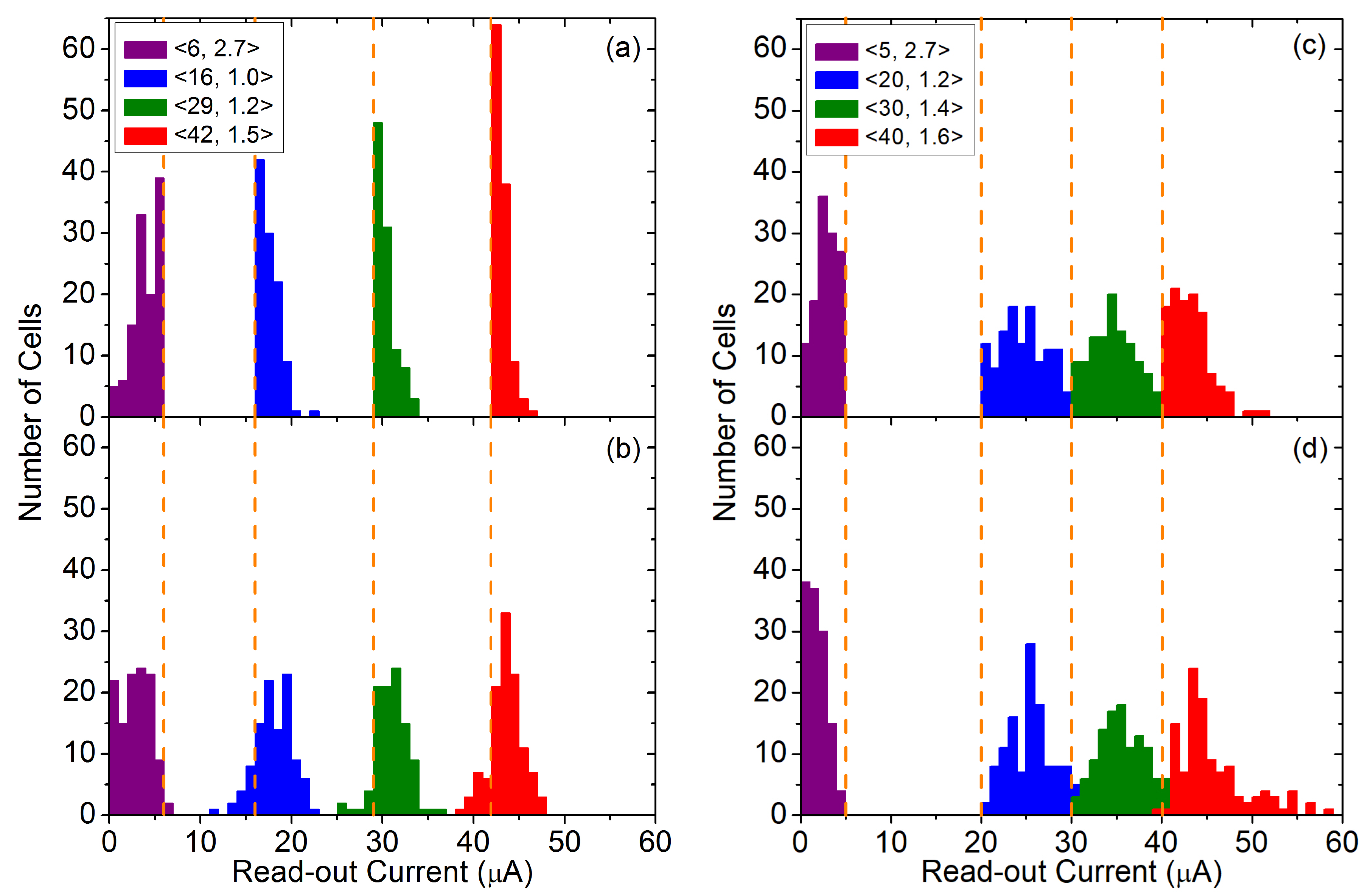
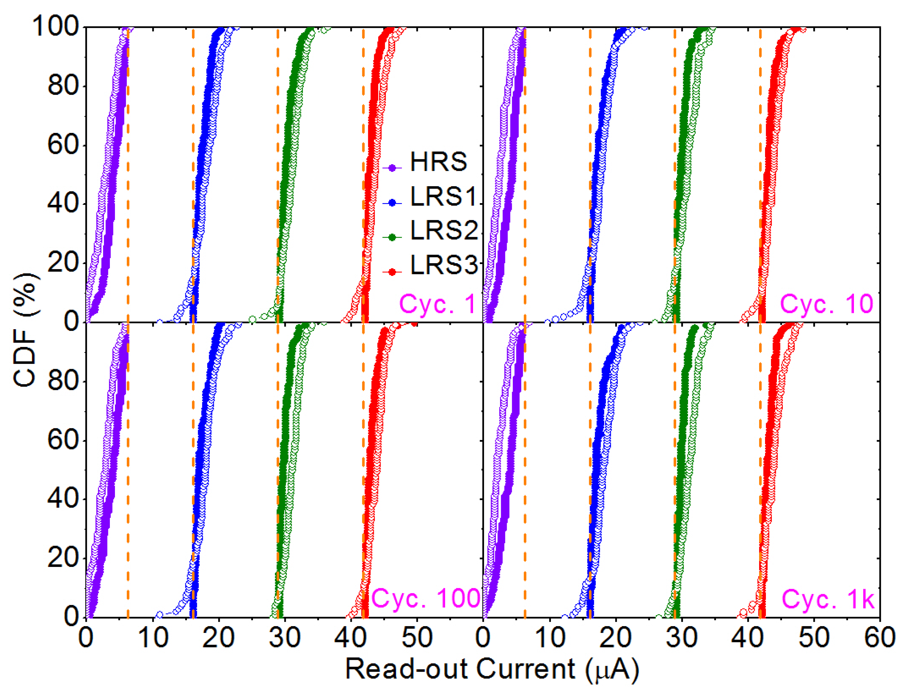
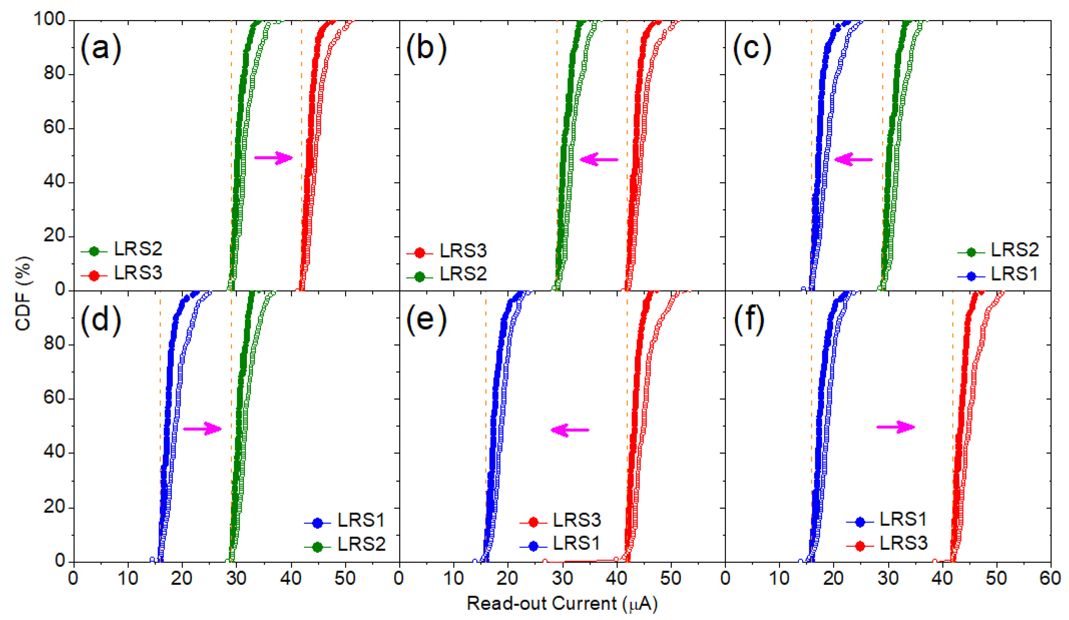
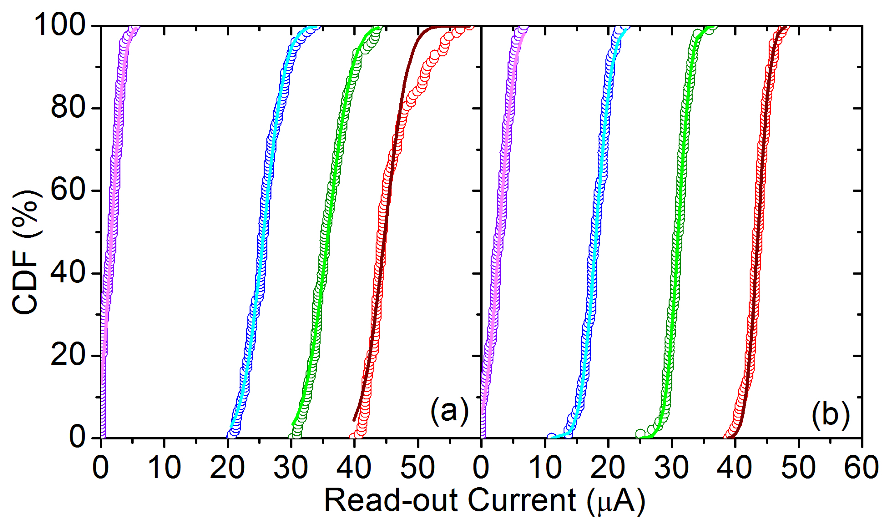
4. Experimental and Modeling Results

After applying the forming operation in three steps, the experimental read-out current distributions obtained for the four conductive levels, namely, HRS, LRS1, LRS2, and LRS3 by using the optimized combination of M-ISPVA parameters are shown in Figure 2a,b as histograms. The distributions illustrated in Figure 2a correspond to the read-out current values measured just after the I t r g is overcome. No overlap between conductive levels is reported. Since the read-verify operations are continuously performed on the whole batch of 128 RRAM devices (even on RRAM cells already successfully switched) until the M-ISPVA finishes, post-algorithm instabilities can lead to perturbations on the conductive state originally programmed. The distributions measured at the end of the M-ISPVA are shown in Figure 2b. Only a slight reorganization of the read-out current distributions is observed while the lack of overlap between contiguous conductive levels is still maintained. On the other hand, the read-out current distributions illustrated in Figure 2c,d regarding the use of non-optimized M-ISPVA parameters [26] show a small but evident overlap between the three LRS distributions in both cases, namely, just after the switching (Figure 2c) and at the end of the M-ISVPA execution (Figure 2d). Therefore, a careful selection of the < I t r g , V g > values for each conductive level leads indeed to a reliable definition of discrete conductive levels in RRAM arrays.
Once the optimized combination of programming parameters was experimentally proved to successfully define non-overlapped conductive levels despite the inherent DTD variability present on HfO 2 -based RRAM arrays [37,38], the stability of the four conductive levels during the subsequent switching cycles was tested. An endurance test consisting of 1 k reset-set cycles between the HRS and the corresponding LRS was carried out on each batch of 128 RRAM devices in order to assess the CTC variability. As shown in Figure 3, the experimentally measured read-out current CDFs associated with each of the four conductive levels remain essentially unchanged along the whole endurance test. The existing CTC variability has no significant impact on the definition of the four conductive levels as the switching cycles go by.
In order to further assess the CTC variability, the switching between conductive levels was experimentally tested in a way hardly shown in the literature, namely, the inter-levels switching. All possible LRS-LRS transitions (by using the HRS as an intermediate step) were carried out on the same batch of 128 RRAM devices. In Figure 4, the CDFs of the experimentally measured read-out currents for the three LRS conductive levels are shown before and after, respectively, performing each one of the six possible LRS-LRS transitions. All transitions were successfully accomplished independently of the particular history of conductive levels previously programmed on the RRAM batch.
Finally, the experimental CDFs corresponding to the read-out current distributions depicted in Figure 2b,d, that is, the values measured at the end of the M-ISPVA for the optimized and non-optimized combination of programming parameters, respectively, were fitted by using the behavioral model presented previously. As Figure 5 illustrates, the Gaussian curves fit with very high accuracy the experimental data for all four conductive levels in both programming approaches. The average ( μ ) and standard deviation ( σ ) values for the fitting Gaussian CDFs are summarized in Table 2.

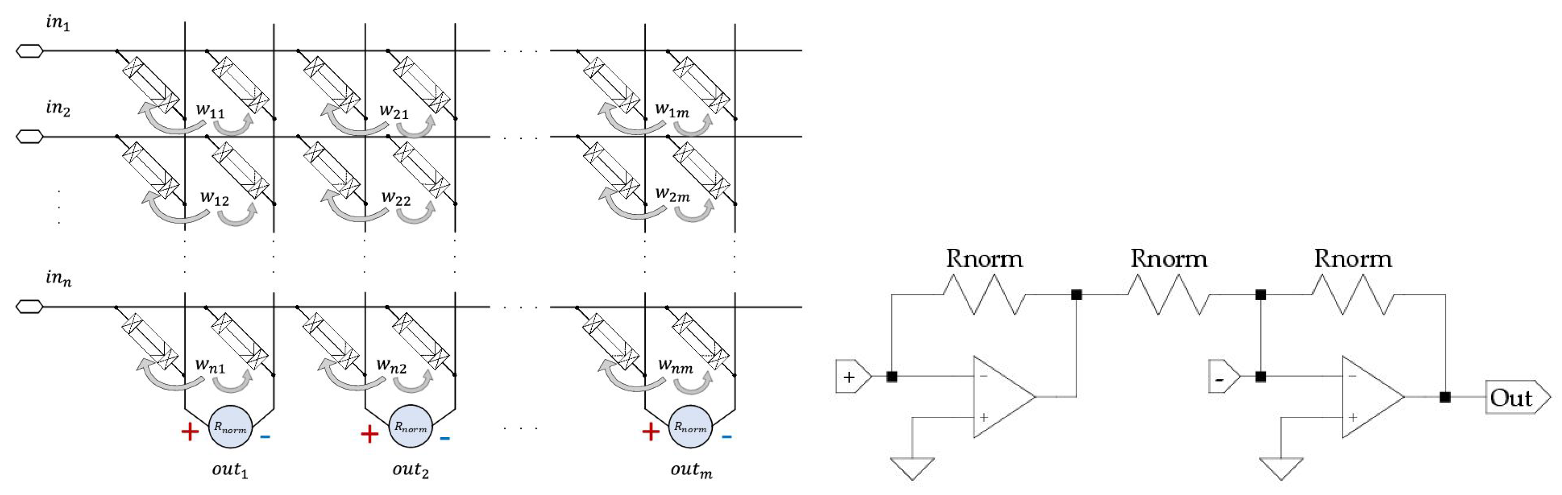
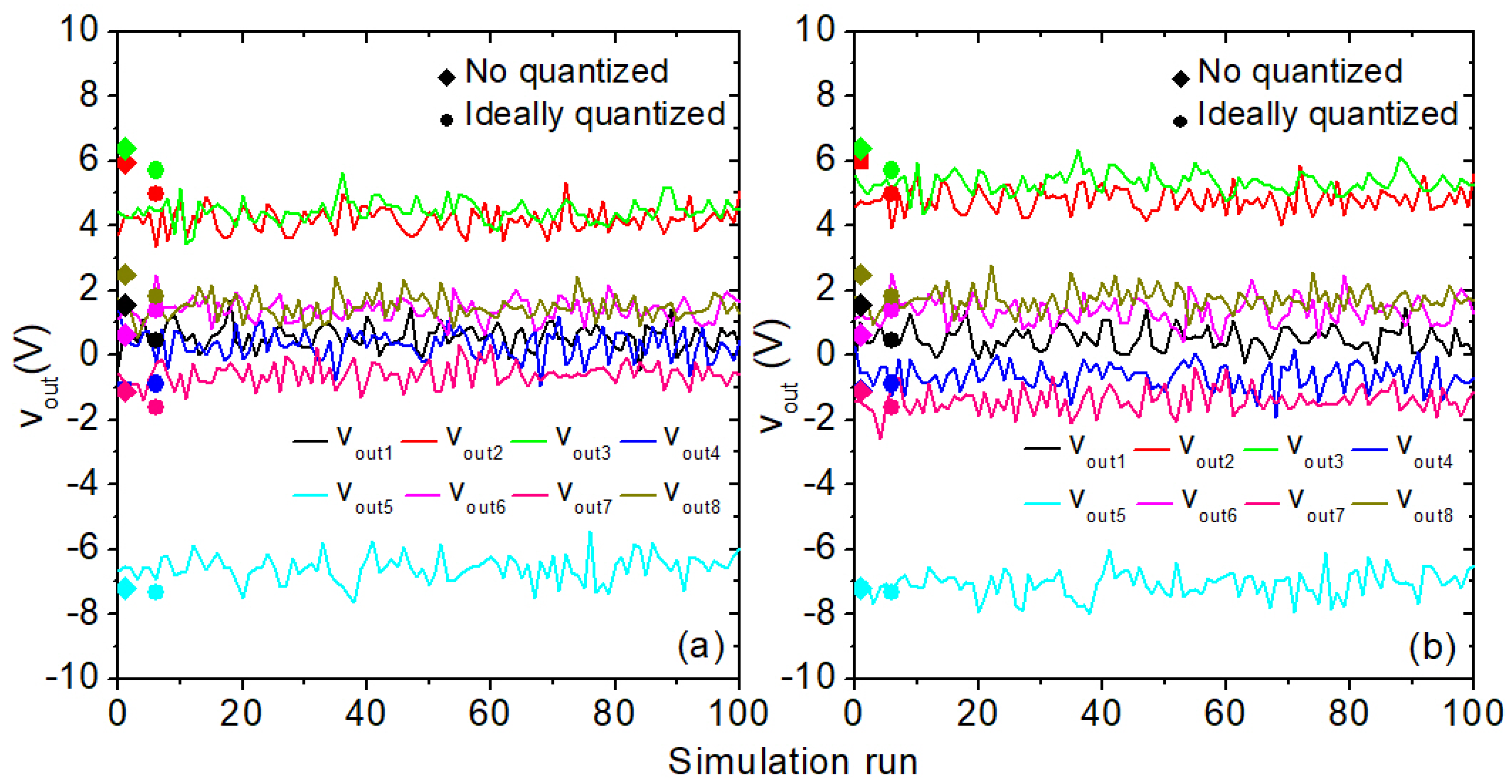
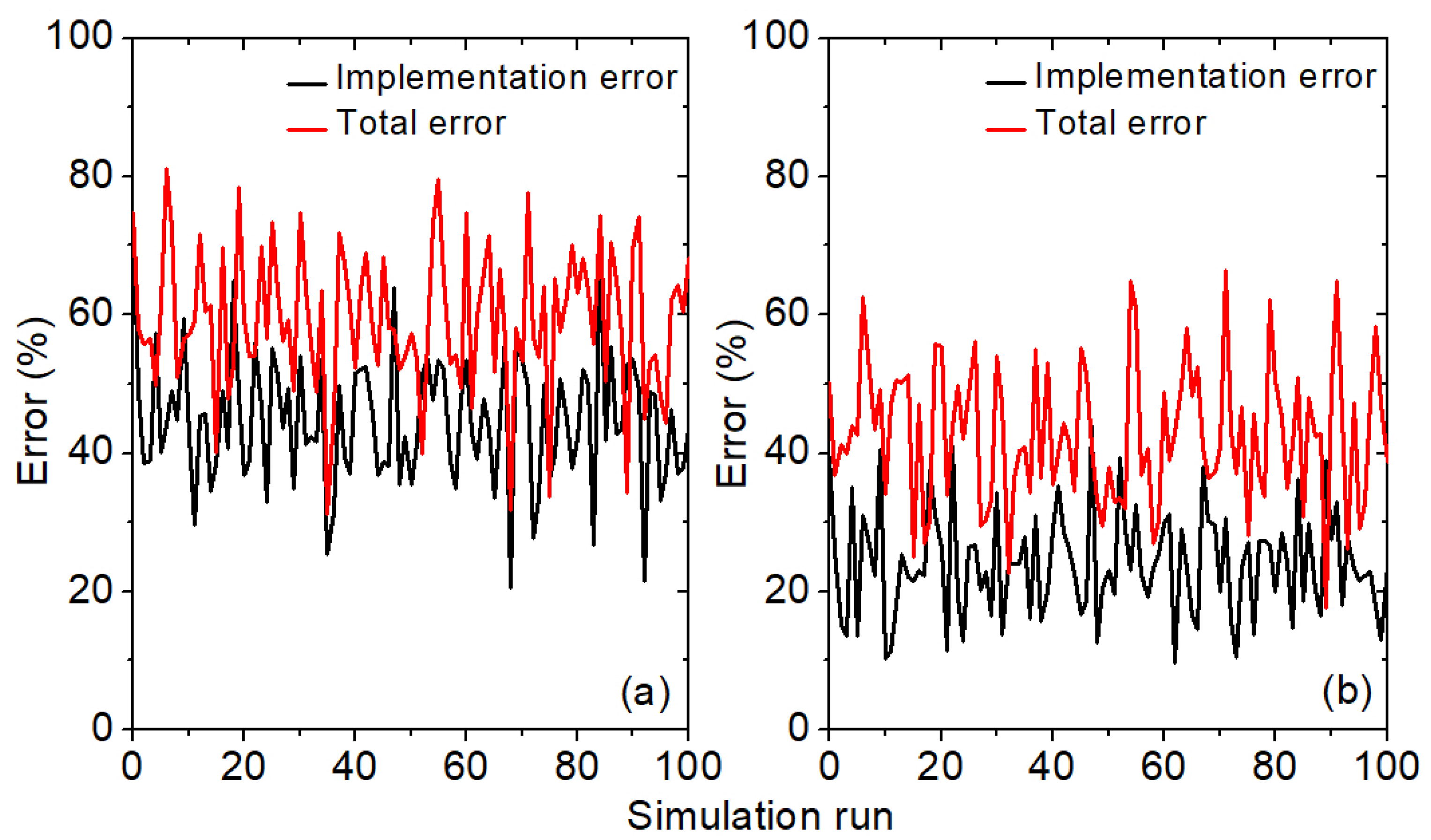
5. VMM Architecture and Operational Results

In order to evaluate the impact of the variability featured by the conductive levels defined on RRAM arrays in a realistic scenario, in particular, the variability reduction by optimizing the programming parameters, a 8 × 8 VMM hardware accelerator has been simulated. In Figure 6 (left), a schematic of the architecture used to implement the VMM is depicted. Each synaptic weight in the matrix is implemented in differential fashion by means of two 1T1R RRAM devices, each one of which defines its conductive value according to the behavioral model (Figure 5) described in [34]. The differential approach let us effectively increase the number of discrete weight values per synapse (up to seven) as well as to deal with positive and negative coefficients without any additional computation step. Hence, the output value for each column is calculated at the bottom by a weighted adder as depicted schematically in Figure 6 (right). The contribution of the input voltages v i n i to each output voltage v o u t j matches the following term:
v o u t j = i = 1 n v i n i · 1 R i j + 1 R i j R n o r m ,
where R i j + ( R i j ) is the resistance of the RRAM device connected to the positive (negative) adder input, 1 R i j + 1 R i j R n o r m w i j are the weight values and R n o r m is a scale factor in the adder. For positive weights, the negative RRAM device is programmed in the HRS, while the positive RRAM device is programmed in one of the four conductive levels. On the other hand, negative weights require that the positive RRAM device is in the HRS, while the negative RRAM device is in any of the four possible conductive levels.
The synaptic weights w i j defined in the 8 × 8 matrix are quantized values (in seven levels) calculated as the x q variable named in Equation (2). The original continuous range quantized x f spans from −10 to 10. Although the experimental CDFs fitted in Figure 5 were obtained at a read-out voltage of 0.2 V, the behavioral model already proved to reproduce well the read-out current CDFs measured during the M-ISPVA programming at different read-out voltages in the range of 0.1–0.5 V (top limit defined to avoid any possible read-out perturbation on the RRAM conductive state) [34]. This feature turns out to be crucial to implement the coefficients of the input vector (applied at i n i ), which will be multiplied with the 8 × 8 matrix.
Several error sources make the circuit outputs to be different from the targeted ones. First of all, the quantization error, which has been reduced by using differential synapses for implementing each matrix weight, is still a hurdle for the hardware implementation of accurate VMM accelerators. Secondly, a normalization error comes up since uniform quantization intervals are used while the conductive levels defined at each RRAM device are not well linearly spaced. Finally, the device variability plays the most crucial role since it additionally impacts quantization and normalization errors. Therefore, the results collected from the VMM simulations will be assessed in terms of the device variability achieved by using one of the two programming approaches, namely, M-ISPVA with non-optimized and optimized < I t r g , V g > pairs of parameters.
The accuracy of the VMM operation was assessed by multiplying an 8 × 8 matrix with a 1×8 vector, both randomly generated in the range from −10 to 10. The vector was mapped into input voltages in the range between 0.0 and 0.5 V, whereas the synaptic weights of the matrix were quantized in seven levels by using Equation (2) and then mapped into the differential RRAM pairs as the corresponding conductive levels. Several Monte Carlo simulations were launched in order to consider the variability featured by the RRAM devices. Figure 7a,b summarize the results of the simulation study (solid lines) by using the non-optimized and the optimized set of M-ISVPA parameters, respectively. In each simulation step, the conductances of the RRAM devices were randomly modified according to the statistical distributions for each level depicted in Figure 5. For a better evaluation of the results, the VMM outputs were also calculated without taking into account the variability, setting the conductance of the RRAM devices at the mean value of the Gaussian distribution for each conductive level. Here, two scenarios were taken into account, namely, no quantized weights in the matrix (square symbols and dashed lines in Figure 7), which produces in fact the exact output values, and ideally quantized weights in the matrix (circle symbols in Figure 7), which omit the errors linked to the fact that experimental RRAM conductive levels are not evenly spaced.
The results illustrated in Figure 7 clearly show that the output values ( v o u t j ) are quite close to the ideal ones. Moreover, the use of the optimized set of programming parameters (Figure 7b) improves the accuracy of the operation significantly compared to the accuracy achieved when using the non-optimized one (Figure 7a). This is due to the fact that the former reduces the variability within each conductive level (avoiding any overlap between them) as well as defines these levels better linearly spaced.
For the sake of a better comparison between these two programming approaches, an average error between the exact result and the real VMM output has been defined as follows:
e r r o r = j = 1 n V o u t j V o u t j 0 V o u t j 0 n · 100 ,
where V o u t j is the voltage value provided by the circuit output j, V o u t j 0 is its corresponding exact value, and n = 8 for our specific VMM circuit. In order to distinguish the quantization error from other error sources, two kinds of errors were defined, namely, the Total error and the Implementation error. The former takes into account the overall error, that is, the exact output V o u t j 0 is the result obtained with no quantized weights, whereas the latter calculates the error considering V o u t j 0 as the result obtained with ideally quantized weights. Therefore, the Implementation error is the contribution to the Total error which is not caused by the quantization of the matrix of weights. Figure 8a,b plot both kind of errors for each simulation step when using non-optimized and optimized programming parameters, respectively. The reduction of the error achieved by optimizing the M-ISPVA parameters is clearly illustrated.

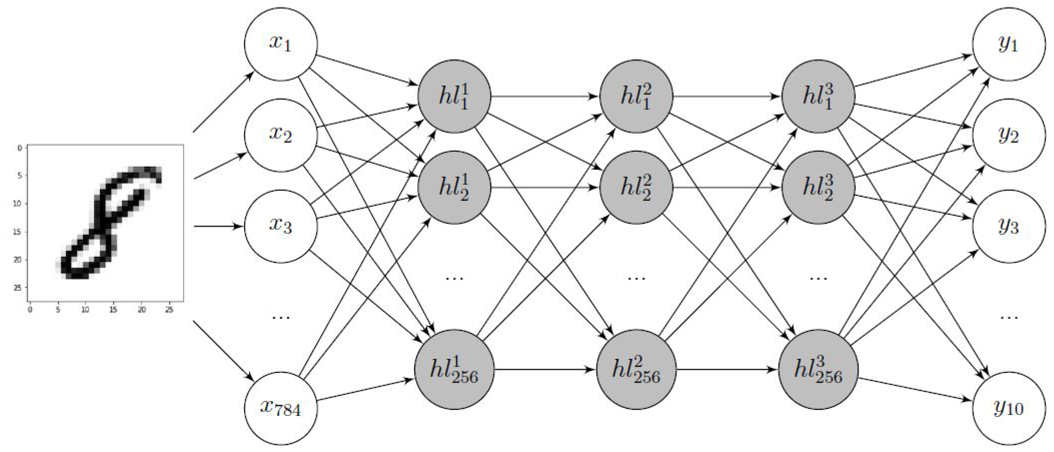
6. DNN Implementation

Finally, the 8 × 8 VMM architecture was extended and integrated in a 4-layer feedforward DNN with the aim of evaluating the impact of the RRAM variability on the accuracy in the classification task of the MNIST database [39]. This classifier is a multi-layer perceptron (MLP) that uses the backpropagation algorithm for optimizing the log-loss function by means of the stochastic gradient descent and ReLU activation functions [40]. The DNN was trained during 500 epochs or until the loss (a prediction error) did not increase by at least 10−4. The architecture employed for implementing the DNN is depicted in Figure 9 and consists of 784 neurons ( x i ) in the input layer (one for each of the 28 × 28 pixels of the MNIST database images), 10 neurons ( y j ) in the output layer (one for each different class), and three hidden layers of 256 neurons ( h l j i ) each. Overall, 334,336 synapses are involved, whose weights were quantized by means of the Uniform-ASYMM scheme. The variability was introduced to the synaptic weights according to Equation (3) after the training and the quantization process.
In order to analyze the influence of the RRAM variability on the throughput of the quantized DNN, the balanced accuracy was calculated, that is, the average of the recall obtained on each class label [41]. It can be estimated as the number of true positives divided by the total number of elements that actually belong to a specific class, namely, a digit in the MNIST database. The average ( μ a ) and standard deviation ( σ a ) values obtained by employing 20 different configurations of synaptic weights, randomly generated according to the experimental variability, are shown in Table 3. An analogous study was carried out for comparison by considering no variability and an ideal quantization of the synaptic weights, which provides an accuracy value of about 75.5%.
In both approaches, the device variability decreased the balanced accuracy, i.e., it made the DNN working less accurately. Nevertheless, the optimized set of programming parameters achieves better results than the non-optimized counterpart: about 6%. Therefore, it is clear that a significant improvement in the classification results of the DNN can be achieved with a careful selection of the programming parameters. This is not an obvious result since it is known that noise and random variability does not affect the outcome of DNNs in the same way as other hardware systems due to the particular features of the neural networks [42]. It is worth highlighting that a few of the 20 attempts performed to implement variability in the synaptic weights produced better balanced accuracy than the ideally quantized DNN without variability (data not shown). This could be considered as a counterintuitive result. However, this issue is caused by the random nature of the variability introduced, which, in some cases, shifts the values of the synaptic weights closer to the optimal DNN without quantization, while, other times, it shifts them in the opposite direction, producing poorer results.

7. Conclusions

In this study, the efficacy of optimizing the selection of parameters employed by the multi-level programming algorithm i evaluated, namely, the M-ISVPA, the gate voltage ( V g ), and the current target ( I t r g ); used in the definition of the conductive levels, i.e., the synaptic weights, in Al:HfO 2 -based RRAM arrays intended to be implemented in-memory computing accelerators. The goodness of the optimization was confirmed based on four different features: (i) effective suppression of overlapping between read-out current distributions of adjacent conductive levels as well as improved linearity of their allocation in the read-out current range; (ii) reliable endurance cycling during at least one thousand cycles together with a successful switching operation between all four possible conductive levels; (iii) precision improvement of VMM operations in a 8 × 8 simulated hardware accelerator; and (iv) about a 6 % improvement on the recognition rates achieved by a simulated 4-layer feedforward DNN dedicated to the classification of the MNIST database.

Author Contributions

Conceptualization, E.P. and J.B.R.; Samples production, M.K.M.; Electrical characterization, E.P. and E.P.-B.Q.; Vector-Matrix-Multiplication architecture, A.J.P.-Á. and F.J.-M.; Neural network implementation, R.R.-Z. and J.B.R.; Original draft preparation, E.P., F.J.-M., R.R.-Z., and J.B.R.; Review and editing, R.R.-Z., J.B.R., F.J.-M., E.P., and C.W.; Supervision, C.W and J.B.R.; Project administration, C.W and J.B.R. All authors have read and agreed to the published version of the manuscript.

Funding

This research was funded by the German Research Foundation (DFG) in the frame of research group FOR2093 and also by the government of Andalusia (Spain) and the FEDER program in the frame of the project A.TIC.117.UGR18. The publication of this article was funded by the Open Access Fund of the Leibniz Association.

Conflicts of Interest

The authors declare no conflict of interest.

Abbreviations

The following abbreviations are used in this manuscript:
RRAMResistive Random Access Memory
M-ISPVAMulti-Level Incremental Step Pulse with Verify Algorithm
VMMVector-Matrix-Multiplication
AIArtificial Intelligence
IoTInternet of Things
DNNDeep Neural Network
SRAMStatic Random Access Memory
I t r g Target Read-out Current
V g Gate Voltage
DTDDevice-to-Device
CTCCycle-to-Cycle
1T1R1-Transistor-1-Resistor
LRSLow Resistive State
WLWord Line
MIMMetal-Insulator-Metal
ALDAtomic Layer Deposition
TEMTransmission Electron Microscopy
BLBit Line
SLSource Line
HRSHigh Resistive State
CFConductive Filament
VASVoltage Amplitude Sweep
PWPulse Width
CDFCumulative Distribution Function
MLPMulti-Layer Perceptron

References

  1. Campbell, M.; Hoane, A.; Hsu, F.H. Deep Blue. Artif. Intell. 2002, 134, 57–83. [Google Scholar] [CrossRef] [Green Version]
  2. LeCun, Y.; Bengio, Y.; Hinton, G. Deep learning. Nature 2015, 521, 436–444. [Google Scholar] [CrossRef]
  3. Wang, F.Y.; Zhang, J.J.; Zheng, X.; Wang, X.; Yuan, Y.; Dai, X.; Zhang, J.; Yang, L. Where does AlphaGo go: From church-turing thesis to AlphaGo thesis and beyond. IEEE/CAA J. Autom. Sin. 2016, 3, 113–120. [Google Scholar] [CrossRef]
  4. Burr, G.W.; Narayanan, P.; Shelby, R.M.; Sidler, S.; Boybat, I.; Di Nolfo, C.; Leblebici, Y. Large-scale neural networks implemented with non-volatile memory as the synaptic weight element: Comparative performance analysis (accuracy, speed, and power). In Proceedings of the 2015 IEEE International Electron Devices Meeting (IEDM), Washington, DC, USA, 7–9 December 2015; pp. 4.4.1–4.4.4. [Google Scholar] [CrossRef]
  5. Mahapatra, N.R.; Venkatrao, B. The processor-memory bottleneck. XRDS: Crossroads ACM Mag. Stud. 1999, 5, 2. [Google Scholar] [CrossRef]
  6. Akopyan, F.; Sawada, J.; Cassidy, A.; Alvarez-Icaza, R.; Arthur, J.; Merolla, P.; Imam, N.; Nakamura, Y.; Datta, P.; Nam, G.J.; et al. TrueNorth: Design and Tool Flow of a 65 mW 1 Million Neuron Programmable Neurosynaptic Chip. IEEE Trans. Comput. Aided Des. Integr. Circuits Syst. 2015, 34, 1537–1557. [Google Scholar] [CrossRef]
  7. Davies, M.; Srinivasa, N.; Lin, T.H.; Chinya, G.; Cao, Y.; Choday, S.H.; Dimou, G.; Joshi, P.; Imam, N.; Jain, S.; et al. Loihi: A Neuromorphic Manycore Processor with On-Chip Learning. IEEE Micro 2018, 38, 82–99. [Google Scholar] [CrossRef]
  8. Di Ventra, M.; Pershin, Y.V. The parallel approach. Nat. Phys. 2013, 9, 200–202. [Google Scholar] [CrossRef]
  9. Ambrogio, S.; Narayanan, P.; Tsai, H.; Shelby, R.M.; Boybat, I.; Di Nolfo, C.; Sidler, S.; Giordano, M.; Bodini, M.; Farinha, N.C.P.; et al. Equivalent-accuracy accelerated neural-network training using analogue memory. Nature 2018, 558, 60–67. [Google Scholar] [CrossRef]
  10. Pei, J.; Deng, L.; Song, S.; Zhao, M.; Zhang, Y.; Wu, S.; Wang, G.; Zou, Z.; Wu, Z.; He, W.; et al. Towards artificial general intelligence with hybrid Tianjic chip architecture. Nature 2019, 572, 106–111. [Google Scholar] [CrossRef]
  11. Kim, K.H.; Gaba, S.; Wheeler, D.; Cruz-Albrecht, J.M.; Hussain, T.; Srinivasa, N.; Lu, W. A functional hybrid memristor crossbar-array/CMOS system for data storage and neuromorphic applications. Nano Lett. 2012, 12, 389–395. [Google Scholar] [CrossRef]
  12. Chu, M.; Kim, B.; Park, S.; Hwang, H.; Jeon, M.; Lee, B.H.; Lee, B.G. Neuromorphic Hardware System for Visual Pattern Recognition With Memristor Array and CMOS Neuron. IEEE Trans. Ind. Electron. 2015, 62, 2410–2419. [Google Scholar] [CrossRef]
  13. Zahari, F.; Hansen, M.; Mussenbrock, T.; Ziegler, M.; Kohlstedt, H. Pattern recognition with TiOx-based memristive devices. AIMS Mater. Sci. 2015, 2, 203–216. [Google Scholar] [CrossRef]
  14. Soudry, D.; Di Castro, D.; Gal, A.; Kolodny, A.; Kvatinsky, S. Memristor-based multilayer neural networks with online gradient descent training. IEEE Trans. Neural Netw. Learn. Syst. 2015, 26, 2408–2421. [Google Scholar] [CrossRef]
  15. Yao, P.; Wu, H.; Gao, B.; Tang, J.; Zhang, Q.; Zhang, W.; Yang, J.J.; Qian, H. Fully hardware-implemented memristor convolutional neural network. Nature 2020, 577, 641–646. [Google Scholar] [CrossRef]
  16. Ielmini, D.; Wong, H.S.P. In-memory computing with resistive switching devices. Nat. Electron. 2018, 1, 333–343. [Google Scholar] [CrossRef]
  17. Wong, H.S.P.; Lee, H.Y.; Yu, S.; Chen, Y.S.; Wu, Y.; Chen, P.S.; Lee, B.; Chen, F.T.; Tsai, M.J. Metal–Oxide RRAM. Proc. IEEE 2012, 100, 1951–1970. [Google Scholar] [CrossRef]
  18. Ielmini, D. Resistive switching memories based on metal oxides: Mechanisms, reliability and scaling. Semicond. Sci. Technol. 2016, 31, 063002. [Google Scholar] [CrossRef]
  19. Bai, Y.; Wu, H.; Wu, R.; Zhang, Y.; Deng, N.; Yu, Z.; Qian, H. Study of multi-level characteristics for 3D vertical resistive switching memory. Sci. Rep. 2014, 4, 5780. [Google Scholar] [CrossRef] [PubMed] [Green Version]
  20. Prakash, A.; Park, J.; Song, J.; Woo, J.; Cha, E.J.; Hwang, H. Demonstration of Low Power 3-bit Multilevel Cell Characteristics in a TaOx-Based RRAM by Stack Engineering. IEEE Electron Device Lett. 2015, 36, 32–34. [Google Scholar] [CrossRef]
  21. Stathopoulos, S.; Khiat, A.; Trapatseli, M.; Cortese, S.; Serb, A.; Valov, I.; Prodromakis, T. Multibit memory operation of metal-oxide bi-layer memristors. Sci. Rep. 2017, 7, 17532. [Google Scholar] [CrossRef] [Green Version]
  22. Liu, J.; Yang, H.; Ma, Z.; Chen, K.; Zhang, X.; Huang, X.; Oda, S. Characteristics of multilevel storage and switching dynamics in resistive switching cell of Al2O3/HfO2/Al2O3 sandwich structure. Semicond. Sci. Technol. 2018, 51, 025102. [Google Scholar] [CrossRef]
  23. Woo, J.; Moon, K.; Song, J.; Kwak, M.; Park, J.; Hwang, H. Optimized Programming Scheme Enabling Linear Potentiation in Filamentary HfO2 RRAM Synapse for Neuromorphic Systems. IEEE Trans. Electron Devices 2016, 63, 5064–5067. [Google Scholar] [CrossRef]
  24. Chen, J.; Wu, H.; Gao, B.; Tang, J.; Hu, X.S.; Qian, H. A Parallel Multibit Programing Scheme With High Precision for RRAM-Based Neuromorphic Systems. IEEE Trans. Electron Devices 2020, 67, 2213–2217. [Google Scholar] [CrossRef]
  25. Luo, Y.; Han, X.; Ye, Z.; Barnaby, H.; Seo, J.S.; Yu, S. Array-Level Programming of 3-Bit per Cell Resistive Memory and Its Application for Deep Neural Network Inference. IEEE Trans. Electron Devices 2020, 67, 4621–4625. [Google Scholar] [CrossRef]
  26. Perez, E.; Zambelli, C.; Mahadevaiah, M.K.; Olivo, P.; Wenger, C. Toward Reliable Multi-Level Operation in RRAM Arrays: Improving Post-Algorithm Stability and Assessing Endurance/Data Retention. IEEE J. Electron Devices Soc. 2019, 7, 740–747. [Google Scholar] [CrossRef]
  27. Milo, V.; Zambelli, C.; Olivo, P.; Perez, E.; Ossorio, O.G.; Wenger, C.; Ielmini, D. Low-energy inference machine with multilevel HfO2 RRAM arrays. In Proceedings of the ESSDERC 2019—49th European Solid-State Device Research Conference (ESSDERC), Cracow, Poland, 23–26 September 2019; pp. 174–177. [Google Scholar] [CrossRef]
  28. Milo, V.; Zambelli, C.; Olivo, P.; Pérez, E.; Mahadevaiah, K.M.; Ossorio, G.O.; Wenger, C.; Ielmini, D. Multilevel HfO2-based RRAM devices for low-power neuromorphic networks. APL Mater. 2019, 7, 081120. [Google Scholar] [CrossRef] [Green Version]
  29. Jiang, H.; Han, L.; Lin, P.; Wang, Z.; Jang, M.H.; Wu, Q.; Barnell, M.; Yang, J.J.; Xin, H.L.; Xia, Q. Sub-10 nm Ta Channel Responsible for Superior Performance of a HfO2 Memristor. Sci. Rep. 2016, 6, 28525. [Google Scholar] [CrossRef] [Green Version]
  30. Zhao, M.; Wu, H.; Gao, B.; Zhang, Q.; Wu, W.; Wang, S.; Xi, Y.; Wu, D.; Deng, N.; Yu, S.; et al. Investigation of Statistical Retention of Filamentary Analog RRAM for Neuromorphic Computing. In Proceedings of the IEEE International Electron Devices Meeting (IEDM), San Francisco, CA, USA, 2–6 December 2017; pp. 39.4.1–39.4.4. [Google Scholar] [CrossRef]
  31. Shim, W.; Luo, Y.; Seo, J.S.; Yu, S. Impact of Read Disturb on Multilevel RRAM based Inference Engine: Experiments and Model Prediction. In Proceedings of the 2020 IEEE International Reliability Physics Symposium (IRPS), Dallas, TX, USA, 28 April–30 May 2020; pp. 1–5. [Google Scholar] [CrossRef]
  32. Grossi, A.; Zambelli, C.; Olivo, P.; Miranda, E.; Stikanov, V.; Walczyk, C.; Wenger, C. Electrical characterization and modeling of pulse-based forming techniques in RRAM arrays. Solid-State Electron. 2016, 115, 17–25. [Google Scholar] [CrossRef] [Green Version]
  33. Pérez, E.; Mahadevaiah, M.K.; Zambelli, C.; Olivo, P.; Wenger, C. Characterization of the interface-driven 1st Reset operation in HfO2-based 1T1R RRAM devices. Solid-State Electron. 2019, 159, 51–56. [Google Scholar] [CrossRef]
  34. Perez-Avila, A.J.; Gonzalez-Cordero, G.; Perez, E.; Quesada, E.P.B.; Kalishettyhalli Mahadevaiah, M.; Wenger, C.; Roldan, J.B.; Jimenez-Molinos, F. Behavioral modeling of multilevel HfO2-based memristors for neuromorphic circuit simulation. In Proceedings of the 2020 XXXV Conference on Design of Circuits and Integrated Systems (DCIS), Segovia, Spain, 18–20 November 2020; pp. 1–6. [Google Scholar] [CrossRef]
  35. Miranda, E.A.; Walczyk, C.; Wenger, C.; Schroeder, T. Model for the Resistive Switching Effect in HfO2 MIM Structures Based on the Transmission Properties of Narrow Constrictions. IEEE Electron Device Lett. 2010, 31, 609–611. [Google Scholar] [CrossRef]
  36. Nayak, P.; Zhang, D.; Chai, S. Bit Efficient Quantization for Deep Neural Networks. arXiv 2019, arXiv:1910.04877. [Google Scholar]
  37. Fantini, A.; Goux, L.; Degraeve, R.; Wouters, D.J.; Raghavan, N.; Kar, G.; Belmonte, A.; Chen, Y.Y.; Govoreanu, B.; Jurczak, M. Intrinsic switching variability in HfO2 RRAM. In Proceedings of the 2013 5th IEEE International Memory Workshop, Monterey, CA, USA, 26–29 May 2013; pp. 30–33. [Google Scholar] [CrossRef]
  38. Grossi, A.; Nowak, E.; Zambelli, C.; Pellissier, C.; Bernasconi, S.; Cibrario, G.; El Hajjam, K.; Crochemore, R.; Nodin, J.F.; Olivo, P.; et al. Fundamental variability limits of filament-based RRAM. In Proceedings of the 2016 IEEE International Electron Devices Meeting (IEDM), San Francisco, CA, USA, 3–7 December 2016; pp. 4.7.1–4.7.4. [Google Scholar] [CrossRef]
  39. LeCun, Y.; Cortes, C.; Burges, C.J. The MNIST Database of Handwritten Digits. 1999. Available online: http://yann.lecun.com/exdb/mnist/ (accessed on 5 April 2021).
  40. Popescu, M.C.; Balas, V.E.; Perescu-Popescu, L.; Mastorakis, N. Multilayer perceptron and neural networks. WSEAS Trans. Circuits Syst. 2009, 8, 579–588. [Google Scholar]
  41. Brodersen, K.H.; Ong, C.S.; Stephan, K.E.; Buhmann, J.M. The Balanced Accuracy and Its Posterior Distribution. In Proceedings of the 2010 20th International Conference on Pattern Recognition, Istanbul, Turkey, 23–26 August 2010; pp. 3121–3124. [Google Scholar] [CrossRef]
  42. Covi, E.; Brivio, S.; Serb, A.; Prodromakis, T.; Fanciulli, M.; Spiga, S. Analog Memristive Synapse in Spiking Networks Implementing Unsupervised Learning. Front. Neurosci. 2016, 10, 482. [Google Scholar] [CrossRef] [PubMed] [Green Version]
Figure 1. Cross-sectional transmission electron microscopy (TEM) image and schematic of the 1T1R memory cell (left) and block diagram and micrograph of the 4-kbit memory device (right).
Electronics 10 01084 g001
Figure 2. Histograms of the experimental read-out current distributions measured just after the switching transition (ac) and at the end of the M-ISPVA; (bd) for the four optimized conductive levels (a,b): HRS (<6, 2.7>), LRS1 (<16, 1.0>), LRS2 (<29, 1.2>), and LRS3 (<42, 1.5>); and for the four non-optimized conductive levels (c,d): HRS (<5, 2.7>), LRS1 (<20, 1.2>), LRS2 (<30, 1.4>), and LRS3 (<40, 1.6>) [26].
Electronics 10 01084 g002
Figure 3. CDFs of the read-out currents experimentally measured just after the switching transition (solid symbols) and at the end of the M-ISPVA (open symbols) logarithmically sampled (1, 10, 100, and 1 k cycles) during the 1 k cycles endurance test for the four optimized conductive levels.
Electronics 10 01084 g003
Figure 4. CDFs of the experimentally measured read-out currents measured just after the switching operation (solid symbols) and at the end of the M-ISPVA (open symbols) of the three LRS conductive levels before and after the six LRS-LRS possible transitions: LRS2→LRS3 (a), LRS3→LRS2 (b), LRS2→LRS1 (c), LRS1→LRS2 (d), LRS3→LRS1 (e), and LRS1→LRS3 (f).
Electronics 10 01084 g004
Figure 5. CDFs of the read-out currents measured at the end of the M-ISPVA (open symbols) and calculated using Gaussian distributions (solid lines) for the four conductive levels for the non-optimized (a) and the optimized (b) programming approaches.
Electronics 10 01084 g005
Figure 6. Schematic of a VMM accelerator implementation using two RRAM devices for each synaptic weight in differential fashion (left) and of the weighted adder placed at each column (right).
Electronics 10 01084 g006
Figure 7. Results of 100 Monte Carlo simulations of a VMM operation for a given input vector and a given weights matrix (solid lines), when using the non-optimized (a) and the optimized (b) combination of M-ISPVA parameters. The exact results calculated with no quantized weights (square symbols and dashed lines) and the results calculated with ideally quantized weights (circle symbols) are included for comparison.
Electronics 10 01084 g007
Figure 8. Total error (red lines) and Implementation error (black lines) for the 100 Monte Carlo simulations in Figure 7 when using the non-optimized (a) and the optimized (b) set of M-ISVPA programming parameters.
Electronics 10 01084 g008
Figure 9. Schematic of the fully connected DNN architecture with 784 nodes in the input layer ( x i ), 10 nodes in the output layer ( y j ), and three hidden layers (in gray) with 256 perceptron units ( h l j i ) each one.
Electronics 10 01084 g009
Table 1. Summary of M-ISPVA programming parameters used for the non-optimized and the optimized approaches during forming, reset, set, and read-out operations: target read-out current ( I t r g ), gate voltage ( V g ), voltage amplitude sweep (VAS), and pulse width (PW).
Non-OptimizedOptimized
Operation I trg (μA) V g (V)VAS (V)PW (μs) I trg (μA) V g (V)VAS (V)PW (μs)
Forming 421.52.5–5.0 (0.01)10421.52.5–5.0 (0.01)10
Reset62.70.5–2.5 (0.1)162.70.5–2.5 (0.1)1
Set20, 30, 401.2, 1.4, 1.60.5–2.5 (0.1)116, 29, 421.0, 1.2, 1.50.5–2.5 (0.1)1
Read-out-1.70.21-1.70.21
Table 2. Average ( μ ) and standard deviation ( σ ) values (in μA) of the Gaussian fits for each conductive level for the non-optimized and the optimized operation scheme, respectively.
HRSLRS1LRS2LRS3
Non-optimized μ 1.7025.6635.8144.78
σ 1.522.733.032.87
Optimized μ 2.8518.0831.0143.59
σ 1.851.961.601.55
Table 3. Balanced accuracy (average μ a and standard deviation σ a in %) obtained by working with the training and test datasets of the MNIST database for the non-optimized and the optimized programming approaches.
Non-OptimizedOptimized
μ a σ a μ a σ a
Training63.38.569.34.8
Test63.88.569.94.8
Publisher’s Note: MDPI stays neutral with regard to jurisdictional claims in published maps and institutional affiliations.

