Article

Analysis and Design of a Wideband Low-Noise Amplifier with Bias and Parasitic Parameters Derived Wide Bandpass Matching Networks

1
Communication Center, Institute of Microelectronics, Chinese Academy of Sciences, Beijing 100029, China
2
School of Microelectronics, University of Chinese Academy of Sciences, Beijing 100029, China
3
Bureau of Major Scientific and Technological Tasks, Chinese Academy of Sciences, Beijing 100864, China
4
Bureau of Frontier Science and Education, Chinese Academy of Sciences, Beijing 100864, China
5
Beijing Key Laboratory of New Generation Communication RF Chip Technology, Beijing 100029, China
*
Author to whom correspondence should be addressed.
Electronics 2022, 11(4), 633; https://doi.org/10.3390/electronics11040633
Submission received: 17 January 2022 / Revised: 11 February 2022 / Accepted: 14 February 2022 / Published: 18 February 2022
(This article belongs to the Section Microelectronics)

Abstract

:
This paper proposes a 110% relative bandwidth (RBW) low-noise amplifier (LNA) for broadband receivers with flat gain, low noise and high linearity. Bias and parasitic parameters derived wide bandpass (BPDWB) matching networks and a cascode with dual feedbacks are introduced for broadband performance. Matching network design procedures are demonstrated, and results show that the frequency response of the network fits the target impedance well from 1 GHz to 3.5 GHz. The proposed BPDWB network improves the design efficiency and enhances the prediction accuracy of impedance matching. The proposed LNA in 0.25 μm GaAs pseudomorphic high electron mobility transistor (GaAs pHEMT) technology realizes a minimum NF of 0.45 dB at 1.6 GHz where the NF is less than 0.55 dB within the operating frequency band. A flat gain of 22.5–25.2 dB is achieved with the input voltage standing wave ratio (VSWR) below 1.22 and output VSWR less than 2.5. In addition, the proposed LNA has good linearity where the output third-order intercept point (OIP3) is better than +31.5 dBm, and the output 1 dB compression point (OP1dB) is better than +19 dBm over the wide frequency range.

1. Introduction

Modern wireless communication systems are rapidly developing in the direction of multi-carrier, large-capacity and high-speed information transmission. The demand for high-performance transceivers is increasing [1,2,3]. As the first active component of the RF front-end, the properties of the LNA, especially bandwidth, noise and linearity, will directly affect the performance of the receiver [4,5]. In response to various RF applications, wideband LNAs handle multiple operating frequencies within a limited chip area, which greatly improves the integration of the RF front-end and plays an important role in many applications such as mobile communications, CATV, satellite navigation, and so on [6,7,8].
To achieve a balanced performance, the wideband LNA needs to compromise on the strict specifications in a large frequency range, usually several GHz. However, these indicators have a trade-off to each other, which brings challenges to the design of wideband LNAs. Technologies to achieve broad bandwidth with low noise simultaneously are extensively developed and studied [9,10,11,12,13,14]. In [9], a bandwidth-enhanced Darlington amplifier with shunt feedback is adopted to implement a broadband amplifier with flat gain. However, the NF could not be tolerated due to resistance networks at the Darlington structure. In [10], an LNA with a relative bandwidth of 165% is realized based on the cascade amplifier with resistive feedback. The CS with feedback can achieve a flat broadband bandwidth, but the noise caused by the resistance in feedback is unsatisfactory. Reference [11] explores a bandwidth enhancement technique based on inductive peaking. In [12], a method for designing wideband noise matching is presented.
Compared with semiconductor processes like CMOS and GaN, GaAs has excellent RF performance and cost advantages [13,14]. Compared with MOSFET, HBT and other devices, pHEMT devices have better noise performance and thermal stability [15,16]. Compared with HEMT, the pHEMT has lower noise and higher electron mobility [17,18]. Therefore, GaAs pHEMT, with excellent RF characteristics and acceptable cost, was selected in this paper.
In order to achieve the goal of wide bandwidth and low noise simultaneously, this paper proposed a wideband LNA using BPDWB matching networks and cascode topology with dual feedbacks. The proposed BPDWB network incorporates the L/C in the bias circuit and non-ideal parasitic elements into the design of the matching network, which can realize broadband matching and reduce the negative impact of parasitic components on the circuit concurrently.
The paper is organized as follows: Section 2 introduces the design method of the wideband LNA in detail, including the analysis of the cascode amplifier with dual feedbacks and the design process of the BPDWB network. Section 3 presents the simulation and measurement performance of the proposed LNA and compares it with other published works. Finally, conclusions are given in Section 4.

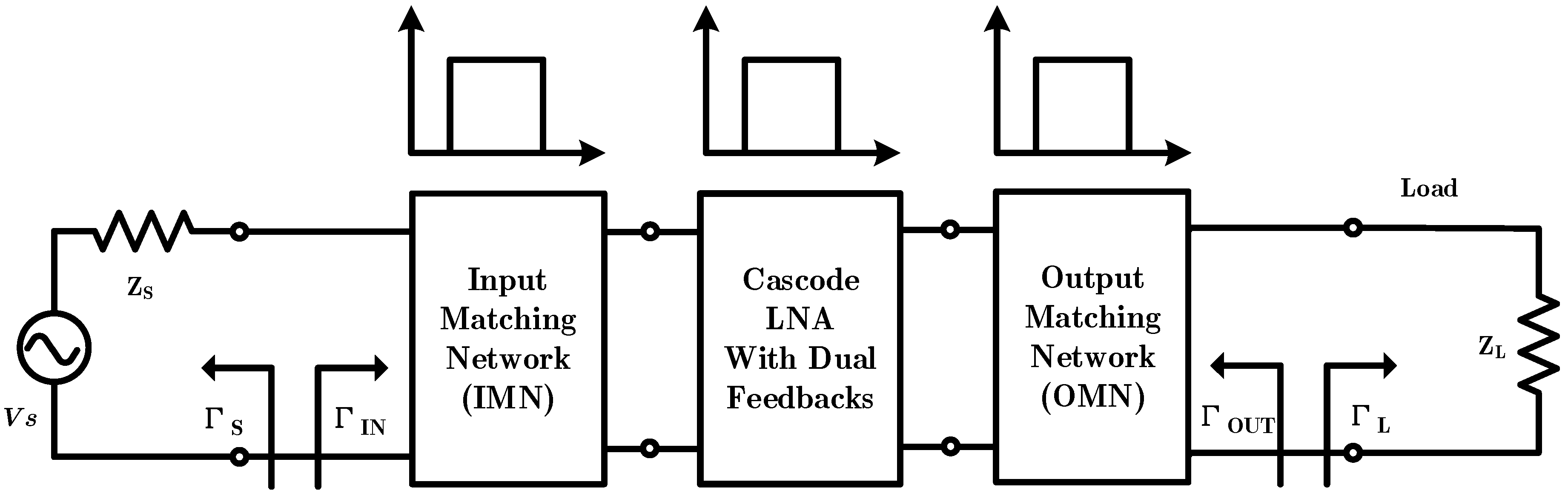
2. Proposed LNA Design

Compared with a narrowband amplifier, a wideband amplifier has the characteristics of large impedance change. To achieve wideband operation, additional circuitry is required. Typically, this means that additional lumped components need to be added to improve the impedance matching of the amplifier to support wideband operation, feedback configuration needs to be added to widen the operable frequency range, or the narrowband amplifier needs to be cascaded [19,20,21]. In this paper, dual feedbacks and bandpass matching networks are combined to expand the bandwidth of LNA and to select the input signal simultaneously. Figure 1 shows the block diagram of the proposed wideband LNA module. The core of LNA is a cascode topology with dual feedbacks, and the input–output matching is a bandpass network using BPDWB, respectively.

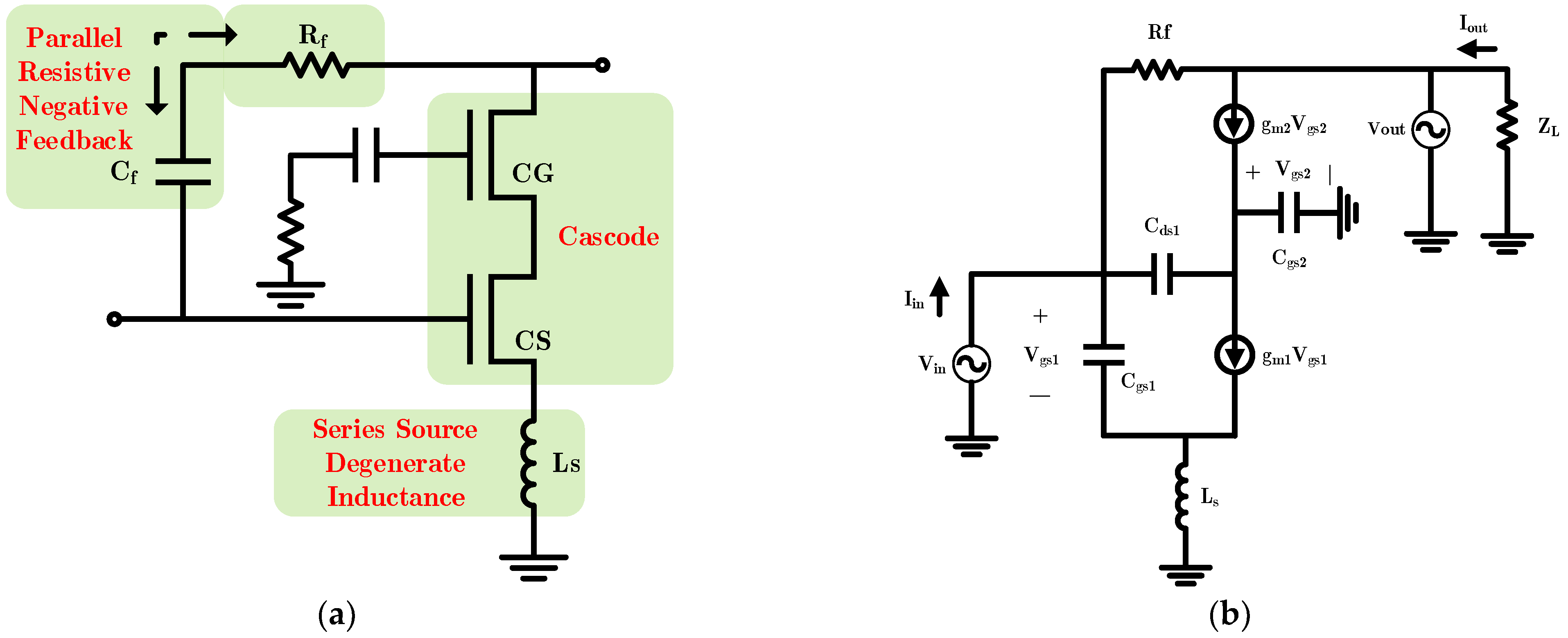
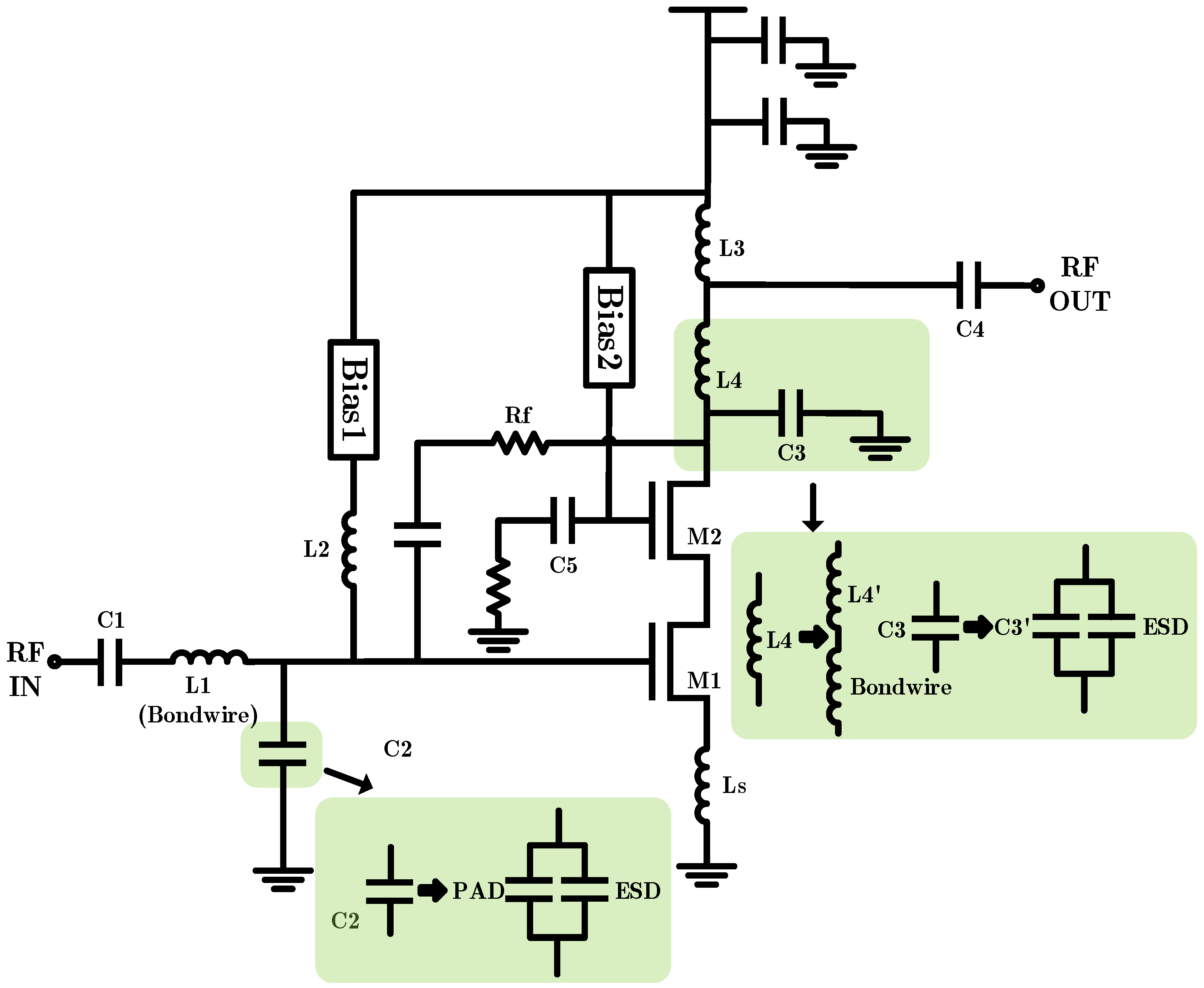
2.1. Cascode with Dual Feedbacks

Linearity and gain are two opposing poles that are difficult to balance, and if we try to improve one, it automatically reduces the other [22]. In this paper, this problem is alleviated by the cascode with feedbacks. The gain of LNA is improved by the stacking of CS and CG, where the Miller effect of CS is cancelled by CG. The linearity is enhanced at the cost of gain by introducing feedback [23]. In short, this approach allows a good compromise between gain and linearity.
In this paper, dual feedbacks (series inductance LS, parallel resistance Rf and capacitance Cf) are connected to the cascode in Figure 2 to achieve high, flat gain and improved linearity.
For the series inductor Ls at the source terminal of CS, a real impedance is introduced to help meet the requirement of input matching and noise matching. In theory, simultaneous noise and input impedance matching can be attained. And there is no impact on the noise performance in the case of ideal inductance [23]. However, due to the non-ideality associated with Ls, additional noise will be introduced to the amplifier. It is necessary to select a suitable value of LS at an acceptable range. When small enough, Ls is often replaced by microstrip lines.
For the parallel negative feedback network between the drain terminal of CG and the gate terminal of CS, it couples the AC signal from the output to the input through the feedback capacitor Cf. The depth of feedback is adjusted by resistor Rf. Since the feedback resistor will also introduce a noise source, the value of the feedback resistor needs to be chosen properly.

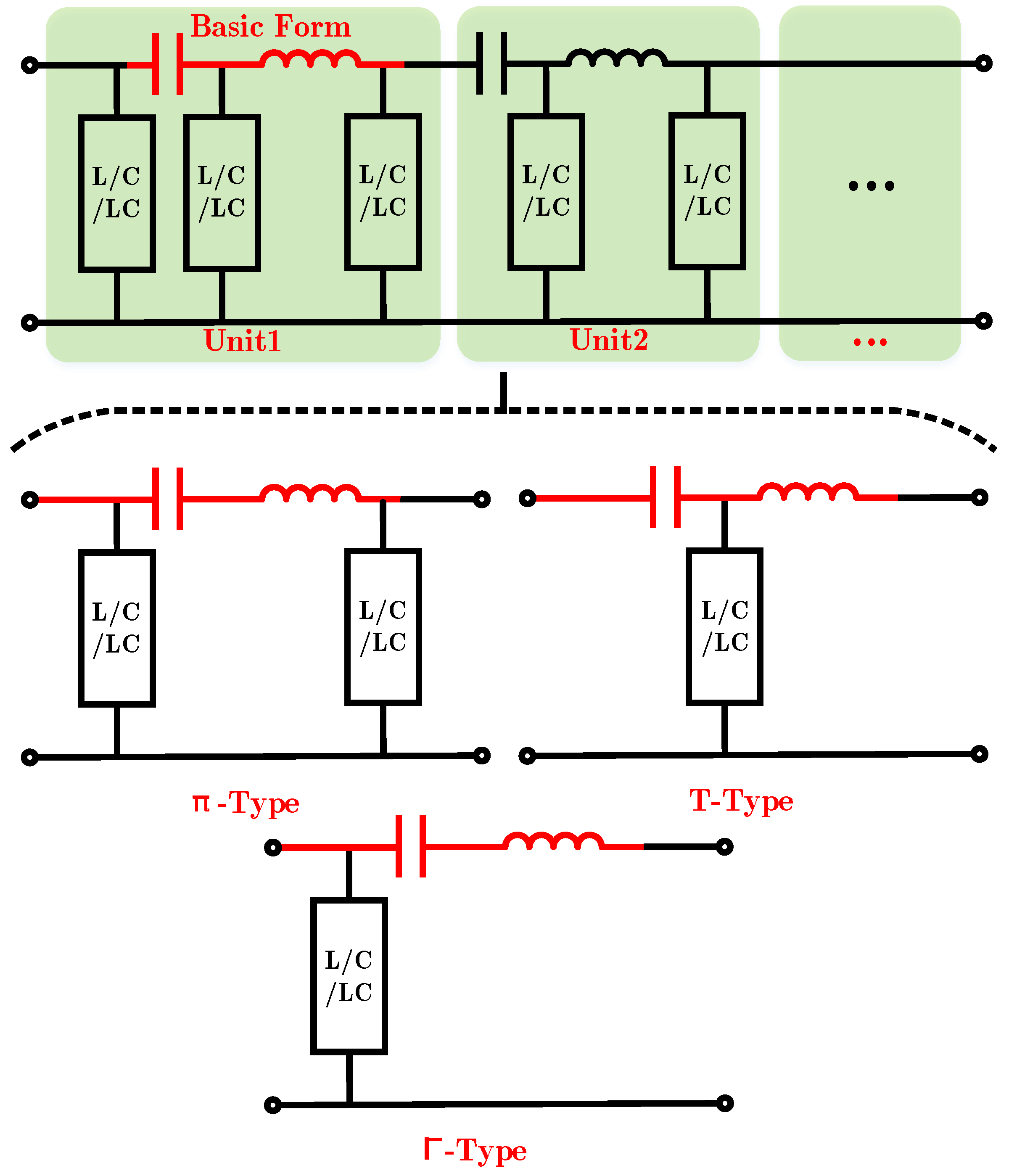
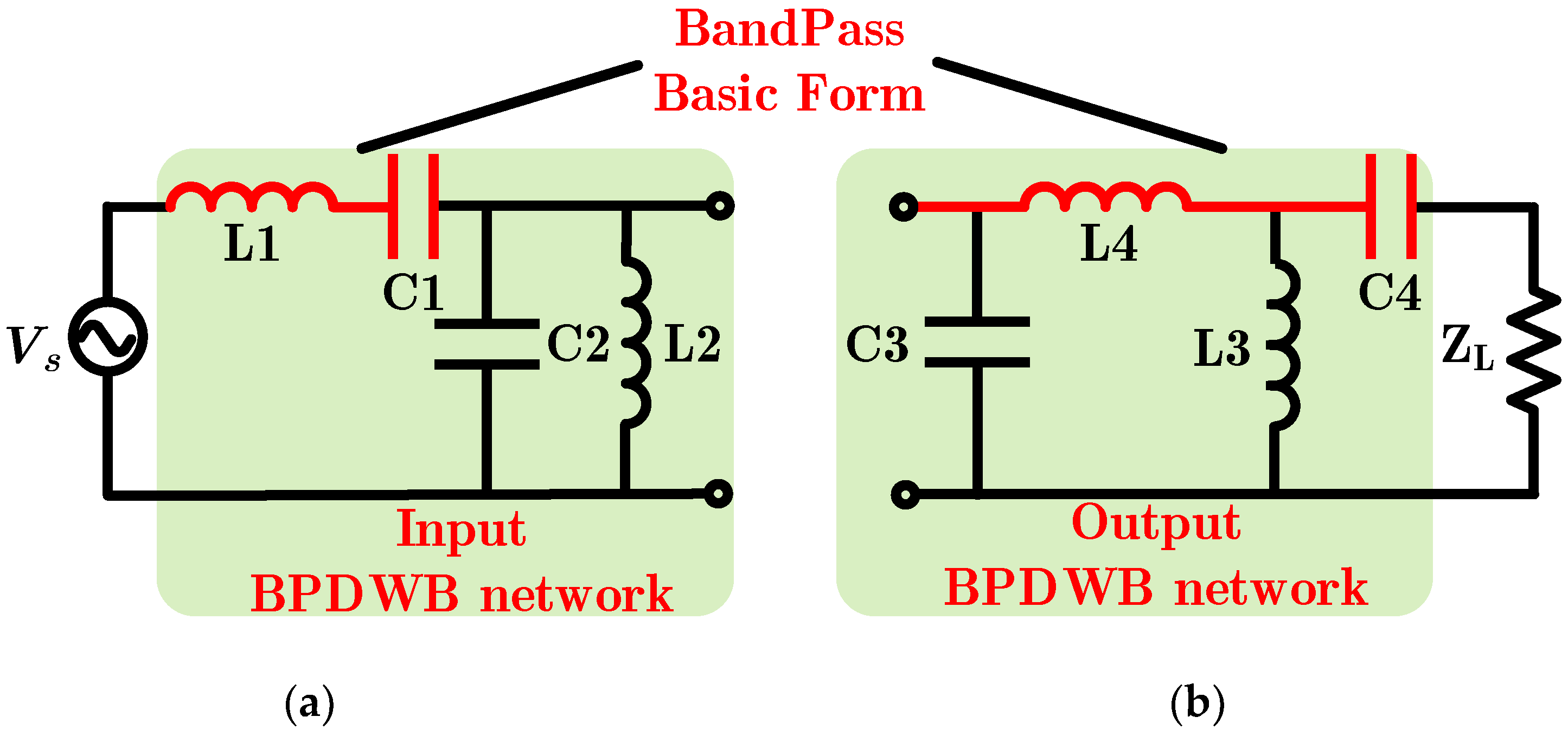
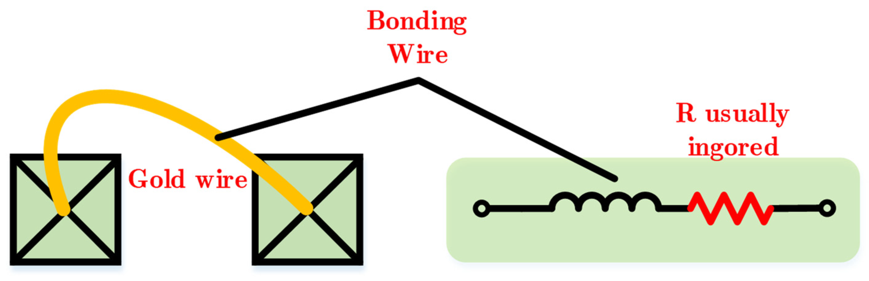
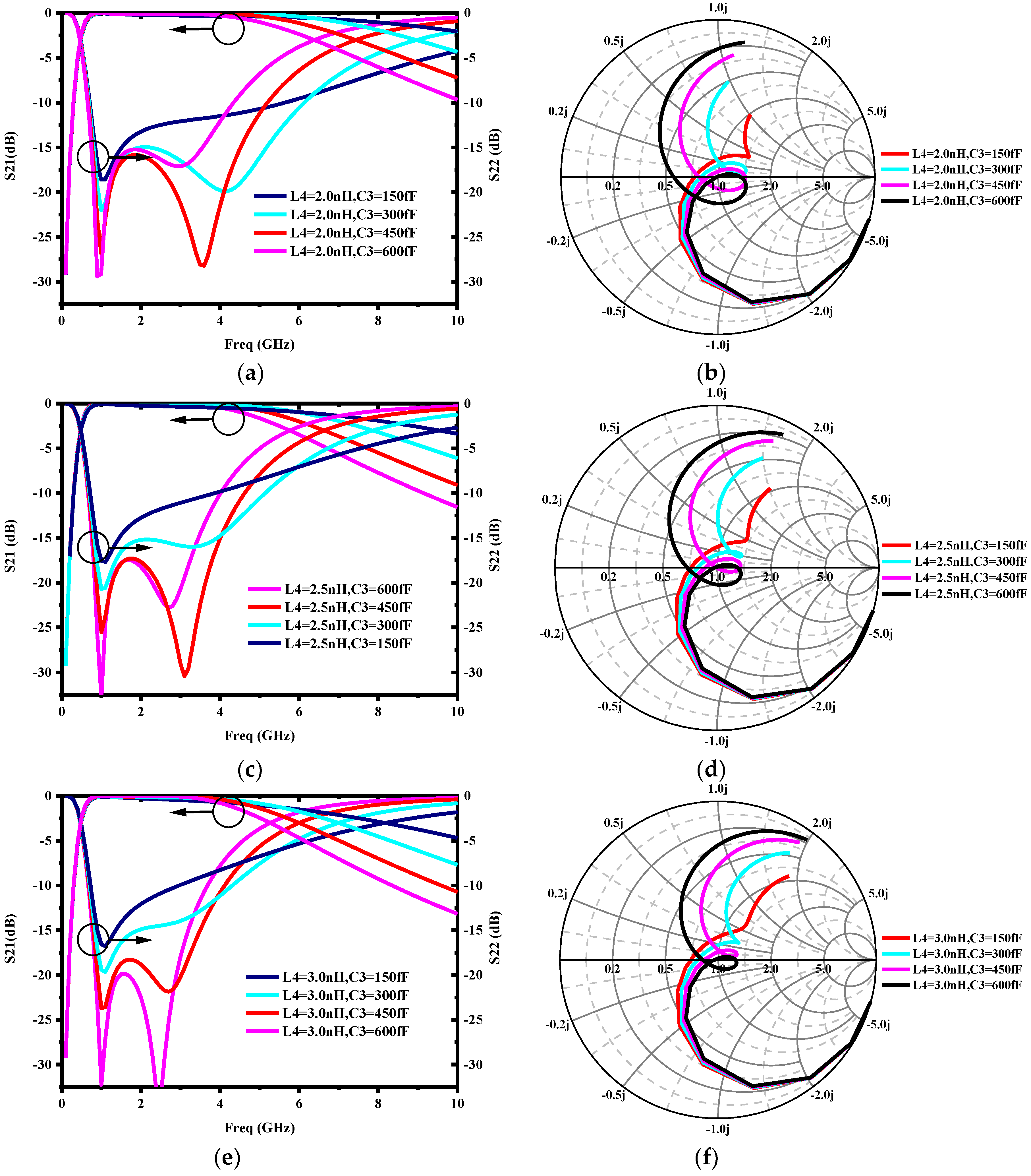
2.2. Bias and Parasitic Parameters Derived Wide Bandpass Matching Network

For the structure in Figure 2b, the input and output impedance can be equivalent to the form of the capacitance and reactance element in parallel, which exhibits capacitive properties at high frequency. For this case, bandpass matching can be used to achieve ideal matching where ideal bandpass filters can be realized by infinite RLC passive components theoretically [24], as shown in Figure 3, divided into basic units. However, the more components used in the circuit design, the more noise and parasitic are introduced. Several common implementations of bandpass matching circuits are shown below.
To achieve the goal of a bandpass matching network without too many lumped components and improve the design accuracy of the matching network, this paper proposes a bandpass filter matching circuit derived from the bias and parasitic parameters named the BPDWB network. A combination of the bias and parasitic elements is used to compose the basic form of the bandpass filter marked in red in Figure 3. After that, the integrated matching network design is completed with the help of the Smith Chart according to the actual needs of impedance transformation. Figure 4 show two possible input and output matching circuits based on BPDWB.
For the input matching network in Figure 4a, it is composed of a series inductor L1 and capacitor C1 with a parallel capacitor C2 and inductor L2. C1 can serve as the input DC block, and L2 as the gate choke inductor. Bonding wire is incorporated into L1. The model of the bonding wire is shown in Figure 5. Its parasitic resistance is usually ignored at RF because it is made of the gold. The capacitor C2 includes the parasitic capacitance at the input such as the PAD and ESD. The output network shown in Figure 4b is composed of L4, C4 in series and C3, L3 in parallel. L3 can be used as a choke inductor and C4 as the output DC block capacitor. C3 includes the parasitic capacitance at the output. C2 and C3 in parallel expand the reactance adjustment range of the matching network so as to fit the frequency response target better.
Once the structure is determined, the frequency response of the network can be determined by analyzing the transmission characteristics. Regarding the network as a two-port network composed of internal unit circuits, the characteristics of the network can be described by the ABCD matrix.
According to the definition of the ABCD matrix, the input network in Figure 4a can be expressed as
[ A B C D ] I M N = [ 1 j ω L 1 0 1 ] [ 1 0 j ω C 2 1 ] [ 1 1 j ω C 1 0 1 ] [ 1 0 1 j ω L 2 1 ] = [ 1 + C 2 C 1 ω 2 C 2 L 1 1 ω 2 C 1 L 2 + L 1 L 2 1 j ω C 1 + j ω L 1 j ω C 2 + 1 j ω L 2 1 ]
The A parameter of the input network can be obtained as
A I M N = 1 + C 2 C 1 ω 2 C 2 L 1 1 ω 2 C 1 L 2 + L 1 L 2
Therefore, the transfer function of the input matching network can be obtained as
S 21 ( ω ) I M N = 2 A I M N = 2 1 + C 2 C 1 ω 2 C 2 L 1 1 ω 2 C 1 L 2 + L 1 L 2
Similarly, the ABCD matrix of the output network in Figure 4b is
[ A B C D ] O M N = [ 1 1 j ω C 4 0 1 ] [ 1 0 1 j ω L 3 1 ] [ 1 j ω L 4 0 1 ] [ 1 0 j ω C 3 1 ] = [ 1 1 ω 2 C 4 L 3 ω 2 C 3 L 4 + C 3 L 4 C 4 L 3 + C 3 C 4 j ω L 4 + L 4 j ω C 4 L 3 + 1 j ω C 4 1 j ω L 3 + j ω C 3 L 4 L 3 + j ω C 3 1 + L 4 L 3 ]
The A parameter of the output network can be obtained as
A O M N = 1 1 ω 2 C 4 L 3 ω 2 C 3 L 4 + C 3 L 4 C 4 L 3 + C 3 C 4
The transfer function of the output matching network is
S 21 ( ω ) O M N = 2 A = 2 1 1 ω 2 C 4 L 3 ω 2 C 3 L 4 + C 3 L 4 C 4 L 3 + C 3 C 4
From Equations (3) and (6), it can be seen that the transfer characteristics of matching circuits are affected by constituent units. The target function can be obtained by tuning the value of components which indicates that the BPDWB network possesses strong tunable performance.

2.3. Design and Implementation of the Wideband Low-Noise Amplifier

Composed of the cascode with dual feedbacks and BPDWB matching networks, the complete circuit of the proposed LNA is shown in Figure 6. LNA is designed with a single positive voltage supply of 5 V. Additionally, the size of the CS and CG transistor is 8 × 75 μm and 8 × 90 μm. The CS and CG is biased at VGS = 0.62 V@VDS = 1.3 V, VGS = 0.52 V@VDS = 3.6 V, respectively.
For expressions (3) and (6), we simplify the analysis by considering the actual situation of the circuit. Since the relation in expressions (7) is:
L 1 < < L 2 ;   C 2 < < C 1
The following items in Equation (3) can be ignored:
C 2 C 1 0 ;   L 1 L 2 0
Thus, Equation (3) can be simplified as
S 21 ( ω ) I M N 2 1 ω 2 C 2 L 1 1 ω 2 C 1 L 2 = 2 ω 2 C 1 L 2 ω 2 C 1 L 2 ω 4 C 1 C 2 L 1 L 2 1
It can be found that expression (9) is mainly determined by C1-L2 on a numerator at low frequency. Therefore, the target transmission characteristics can be achieved by adjusting the value of C1-L2 accompanied by tuning C2 and L1.
As frequency increases, Equation (9) can be abbreviated as
S 21 ( ω ) I M N 2 ω 2 C 1 L 2 ω 2 C 1 L 2 ω 4 C 1 C 2 L 1 L 2 = 2 1 ω 2 C 2 L 1
In Equation (10), the transmission characteristic is mainly affected by the parasitic parameters L1-C2. It shows that the parasitic parameters begin to take effect at high frequencies and deteriorate the transmission performance of the network severely. Therefore, the high cut-off frequency of the matching network can be tuned by controlling the value of parasitic parameters, such as the length of the bond wire.
In addition to the S21 transmission, noise is also an important index that we should consider synchronously.
For noise figures, we know that
F = F M I N + G n R s | Z s Z S O P T | 2
where FMIN is the minimum noise figure, Gn is the noise admittance, Rs is the real part of complex source impedance and ZSOPT is the optimum source impedance.
As the frequency increases, the Cgd of M1 is considered. According to Miller equivalence, Cgd and Rf can be equivalent to the equivalent capacitance and resistance to ground at the input, that is, to contribute to C2 and introduce an equivalent noise source RfM.
  R f M = R f / ( 1 A v )
where AV is the open-loop voltage gain of the amplifier. According to Formula (12), we know that the greater Rf, the greater RfM.
C2 affects the Gn, Rs and ZsZSOPT, thereby deteriorating the NF. Fortunately, we can try to improve this situation by feedbacks. For RfM, the greater its value, the smaller the impact on noise. Therefore, it is necessary to meet the noise requirements by adjusting Ls and selecting an appropriate Rf. Simulation finds that when Rf is greater than 2000 Ω, the effect on noise is no longer obvious. Finally, Rf = 2500 Ω was chosen. On this basis, according to the transmission characteristics and acceptable noise performance, we finally selected Ls ≈ 0.1 nH.
At the output, the capacitance of the DC blocking capacitor C4 is large enough to make the following items close to zero
C 3 L 2 C 4 L 3 0 ;   C 3 C 4 0
Therefore, Equation (6) can be abbreviated as
S 21 ( ω ) O M N 2 1 1 ω 2 C 4 L 3 ω 2 C 3 L 4 = 2 ω 2 C 4 L 3 ω 2 C 4 L 3 ω 4 C 3 C 4 L 3 L 4 1
At low frequencies, the response of the matching network in Equation (14) is mainly affected by C4-L3. At high frequencies, the transfer function can be expressed as Equation (15) which is mainly affected by C3-L4, especially the high cut-off frequency.
S 21 ( ω ) O M N 2 1 ω 2 C 3 L 4
Therefore, the output network can keep constant within the target bandwidth by controlling the tuning C3-C4-L3-L4, especially C3-L4, because high-frequency characteristics are paid special attention to in the design of LNA. In addition, the influence of the output impedance on linearity such as OIP3, should be taken into account in the design of the LNA. According to the two-tone load–pull results, the impedance point for the maximum OIP3 at frequency = 2.2 GHz is Z = 60.6 + j × 12.6 Ω. In order to select the appropriate value of C3-L4 to meet the requirements of output matching and linearity, different combinations of C3-L4 are scanned, and the corresponding results are shown in Figure 7. According to the results, the inductance L4 = 2.5 nH and the capacitance C3 = 300 fF are selected, which can meet the requirements of bandwidth, reflection coefficient and linearity at the same time.
Finally, according to the compromise of each index, the values of each component of the proposed LNA are shown in Table 1.

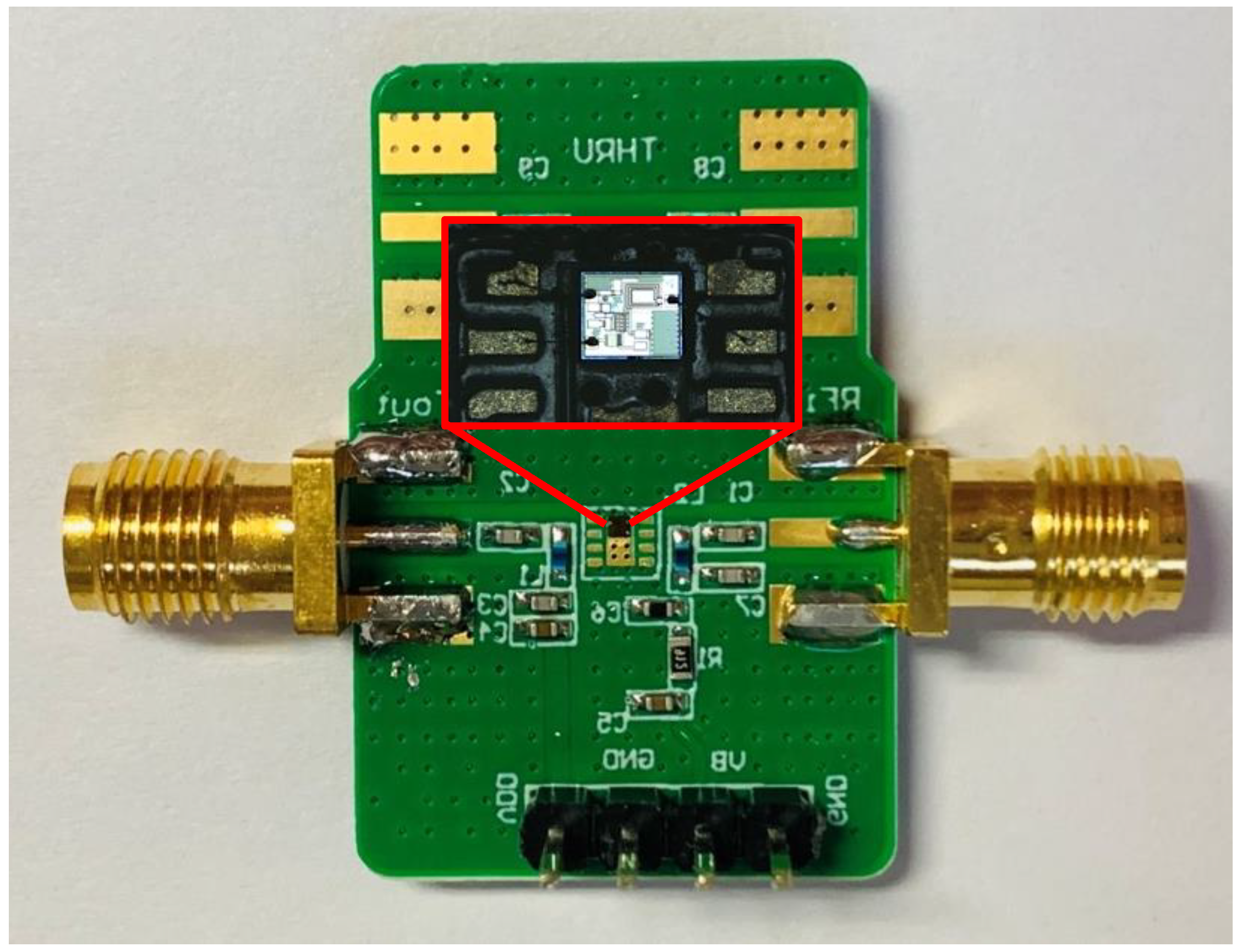
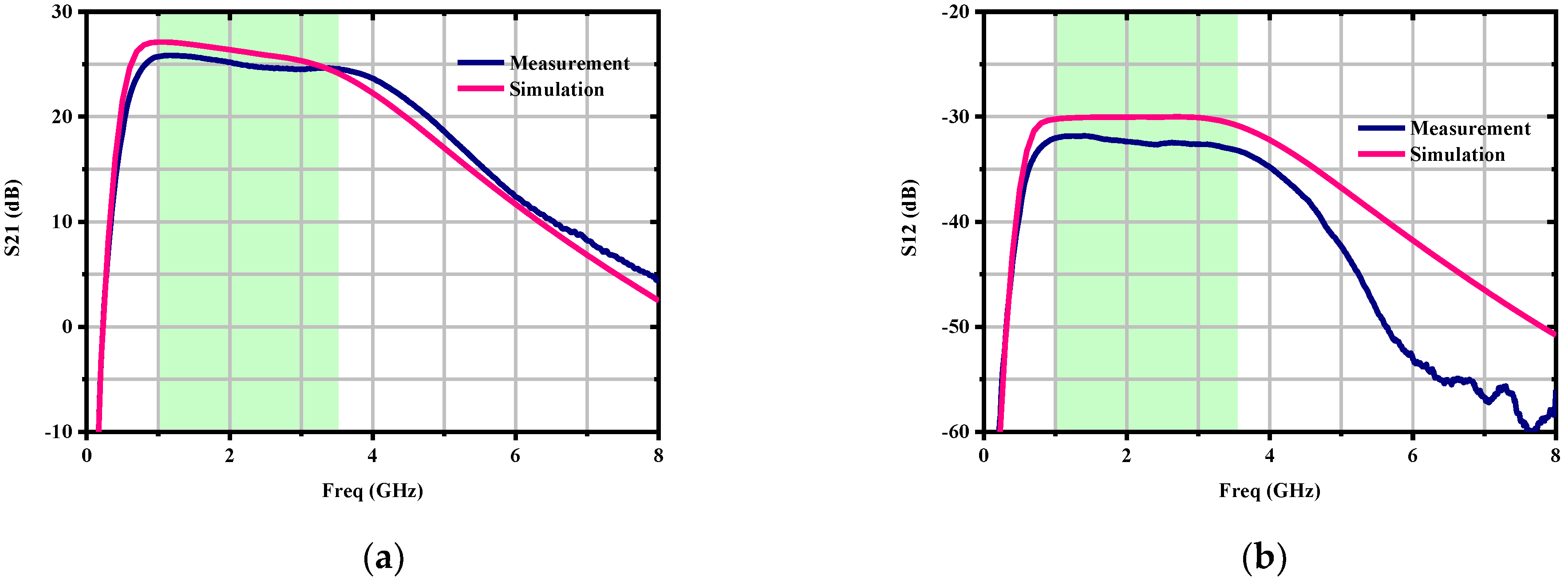
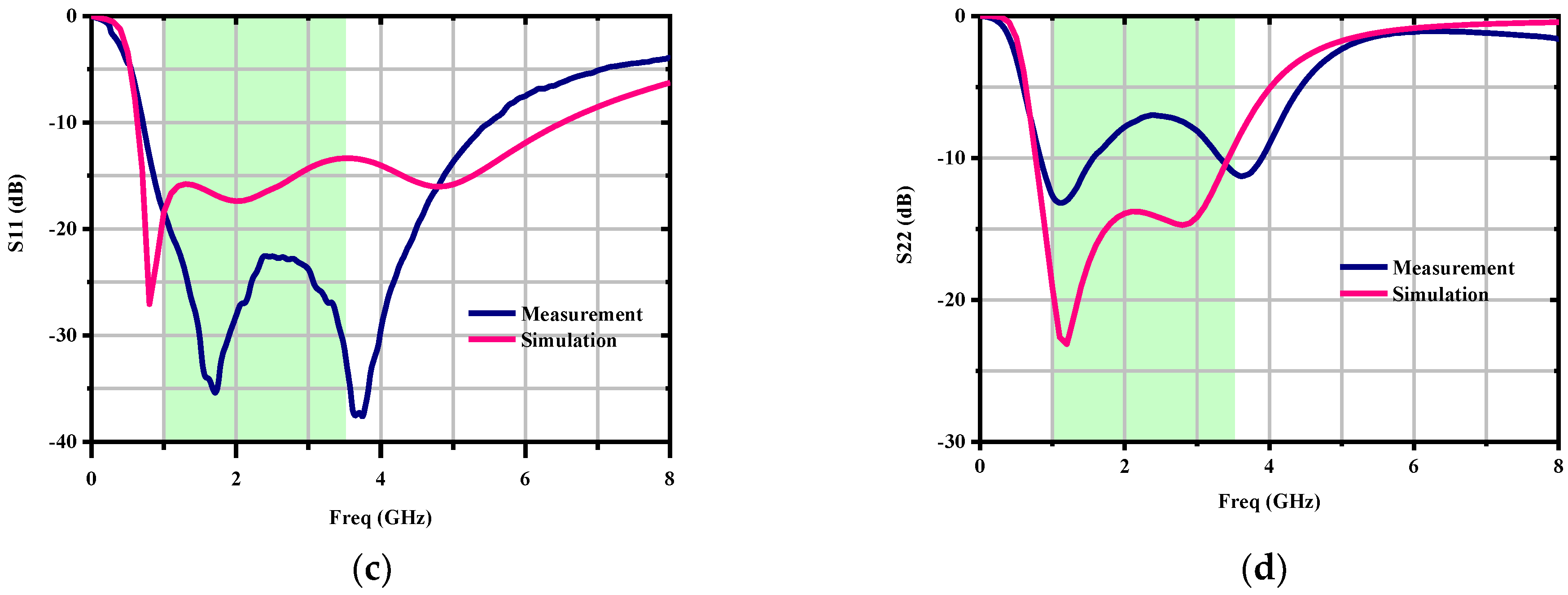
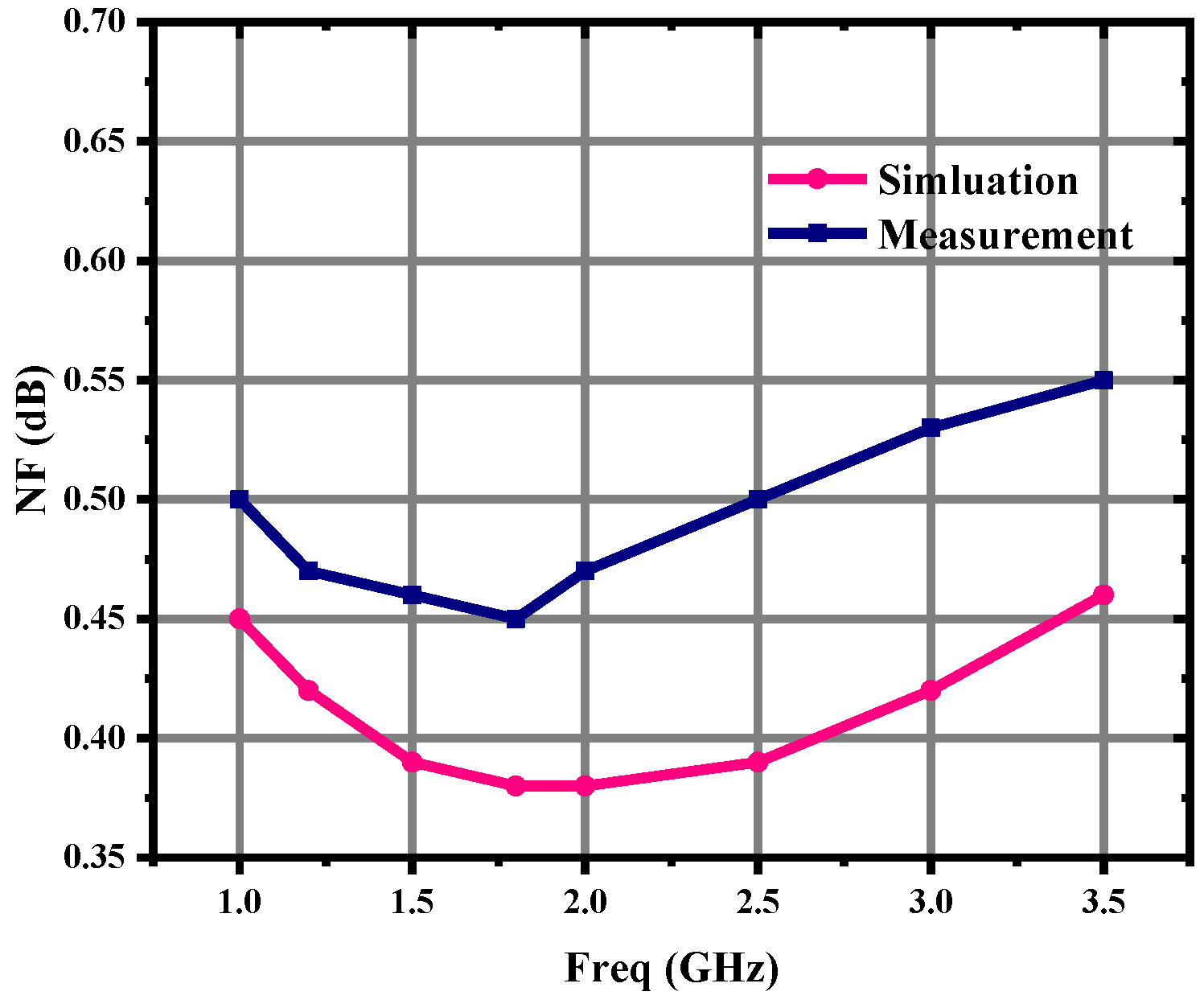
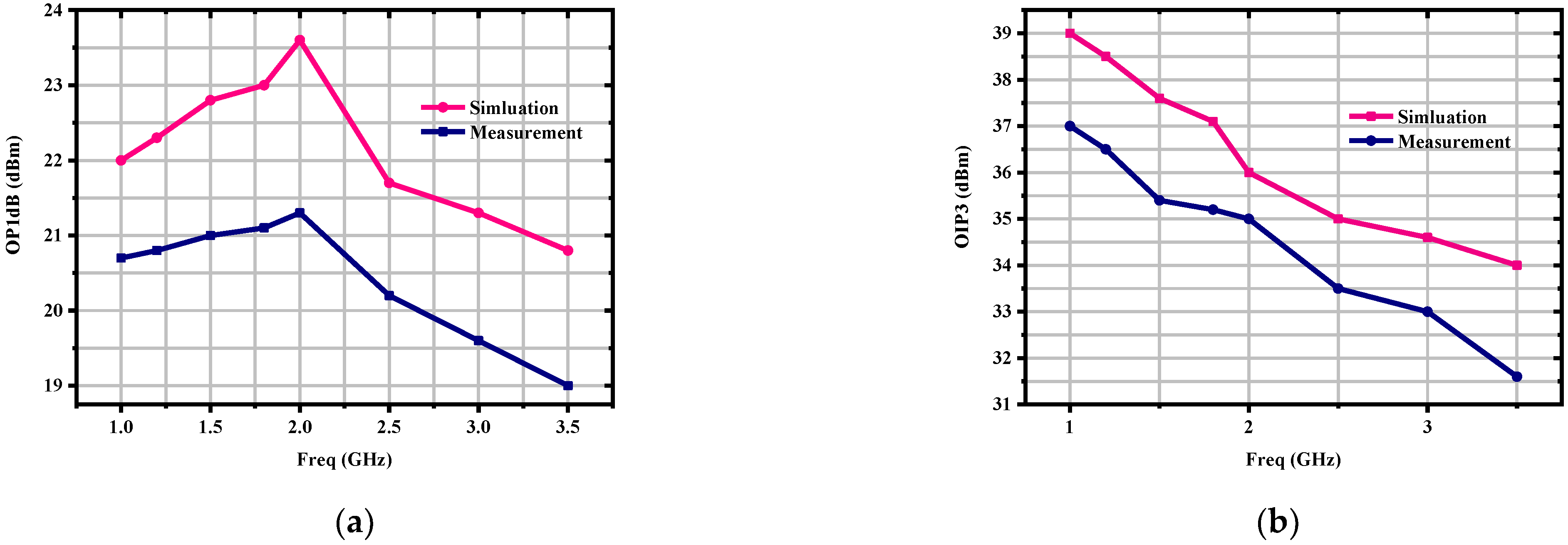
3. Measurement Results

The die and assembly diagram of the chip is shown in Figure 8. The realized LNA is characterized by both linear and non-linear measurements.
To define small-signal behavior, LNA scattering parameters were measured with an Agilent N5230A vector network analyzer. The input/output port of the LNA was designed to be 50 Ω. A PCB test board was developed to simulate practical scenarios, and bond wires were used to connect to the PCB board at each port on the chip. Figure 9 show the measured scattering parameters of the LNA, together with the simulated ones.
From Figure 9, a peak gain of 25.8 dB was measured at 1.2 GHz, which is 1.4 dB lower than the simulated result. Measured S11 and S22 was lower than −20 dB and −7 dB from 1 GHz to 3.5 GHz. As far as S11 and S22 are concerned, the difference between simulation and measurement can be ascribed to the input and output connector and to the coupling parasitic between the devices. The S12 data is lower than −30 dB in the frequency band, indicating that the amplifier had a high level of reverse isolation making the LNA unconditionally stable. Measured scattering parameters demonstrated that the BPDWB network had good prediction accuracy for RF LNA.
For the noise performance, the NF measurement was completed by an Agilent N8975A noise figure meter. A low noise figure (NF) of 0.5 dB (with a ripple of 0.05 dB) was registered in the range from 1 GHz to 3.5 GHz, shown in Figure 10. Compared with simulation data, the measured NF was about 0.1 dB higher. This was caused by the difference between the device and model. And the simulation could not simulate the real conditions of the working device absolutely.
To define large-signal behavior, the linearity measurements were performed for the LNA. Figure 11 present the measured OP1dB and OIP3 results with simulated data according to the single-tone output power test and two-tone third-order intermodulation test. The LNA processes the OP1dB better than +19 dBm and OIP3 greater than +31.5 dBm by 3.5 GHz. Due to transistor large-signal model errors, the measured linearity data is about 2 dB lower than the simulated results.
Table 2 present a comprehensive summary of the performance of the designed wideband LNA and a comparison of the latest works of other published LNAs over the L to S-band.
From the comparison in the table, we can find that in the L-S frequency band, the LNA implemented in this paper within an octave bandwidth has better gain and NF performance than most of the LNAs compared.

4. Conclusions

In this paper, the proposed broadband LNA with the BPDWB network were designed. The theoretical analysis and graphical explanation of the BPDWB design were also discussed. By combining parasitic parameters and bias into BPDWB, the design efficiency and prediction accuracy of the matching circuit were greatly improved. Furthermore, thanks to dual feedbacks, the gain, bandwidth and linearity were also well compromised. The measurement results show that the LNA gain was greater than 22.5 dB and the noise figure less than 0.55 dB from 1 GHz to 3.5 GHz, which verifies the good performance of the proposed LNA and the reliability of the proposed BPDWB network.

Author Contributions

Conceptualization, J.Z., F.W., H.Y., K.W., C.L., J.W., X.L. and Y.Y.; methodology, J.Z., X.L., J.W. and Y.Y.; software, J.Z., F.W. and H.Y.; validation, J.Z., S.Z. and K.W.; data curation, J.Z., F.W. and H.Y.; writing—original draft preparation, J.Z., S.Z. and K.W.; writing—review and editing, J.W., X.L., C.L. and Y.Y.; funding acquisition, X.L. All authors have read and agreed to the published version of the manuscript.

Funding

This research was funded by National Key R&D Program, grant number E0G928C001.

Conflicts of Interest

The authors declare no conflict of interest.

References

  1. Conceição, F.; Gomes, M.; Silva, V.; Dinis, R.; Silva, A.; Castanheira, D. A Survey of Candidate Waveforms for beyond 5G Systems. Electronics 2021, 10, 21. [Google Scholar] [CrossRef]
  2. Motz, C.; Paireder, T.; Pretl, H.; Huemer, M. A Survey on Self-Interference Cancellation in Mobile LTE-A/5G FDD Transceivers. IEEE Trans. Circuits Syst. II Express Briefs 2021, 68, 823–829. [Google Scholar] [CrossRef]
  3. Ijiga, O.E.; Ogundile, O.O.; Familua, A.D.; Versfeld, D.J.J. Review of Channel Estimation for Candidate Waveforms of Next Generation Networks. Electronics 2019, 8, 956. [Google Scholar] [CrossRef] [Green Version]
  4. Kukde, A.A.; Kumaravel, S.; Venkataramani, B. A high linearity folded cascode Low Noise Amplifier for wireless receivers. In Proceedings of the 2014 International Conference on Circuits, Power and Computing Technologies, Nagercoil, India, 20–21 March 2014; IEEE: Piscataway, NY, USA, 2015. [Google Scholar]
  5. Laaouane, H.; Foshi, J.; Bri, S. Design of a low noise amplifier for LTE radio base station receivers. In Proceedings of the 2017 International Conference on Wireless Technologies, Embedded and Intelligent Systems (WITS), Fez, Morocco, 19–20 April 2017; IEEE: Piscataway, NY, USA, 2017. [Google Scholar]
  6. Zhou, J.; Zhang, X.; Yu, Y.; Zhang, L.; Zhao, C.; Liu, H.; Kang, K. A 24–30 GHz CMOS LNA with 2.05 dB NF and 0.6 dB in-band gain ripple for 5G-applications. In Proceedings of the 2018 IEEE MTT-S International Wireless Symposium (IWS), Chengdu, China, 6–10 May 2018; IEEE: Piscataway, NY, USA, 2018; pp. 1–3. [Google Scholar]
  7. Arsalan, M.; Wu, F. LNA design for future S band satellite navigation and 4G LTE applications. Comput. Modeling Eng. Sci. 2019, 119, 249–261. [Google Scholar] [CrossRef] [Green Version]
  8. Mahmood, H.U.; Utomo, D.R.; Han, S.-K.; Kim, J.; Lee, S.-G. A Ku-Band RF Front-End Employing Broadband Impedance Matching with 3.5 dB NF and 21 dB Conversion Gain in 45-nm CMOS Technology. Electronics 2020, 9, 539. [Google Scholar] [CrossRef] [Green Version]
  9. Nikandish, G.; Medi, A. Design and analysis of broadband darlington amplifiers with bandwidth enhancement in GaAs pHEMT technology. IEEE Trans. Microw. Theory Tech. 2014, 62, 1705–1715. [Google Scholar] [CrossRef]
  10. Chien, K.H.; Chiou, H.K. A 0.6–6.2 GHz wideband LNA using resistive feedback and gate inductive peaking techniques for multiple standards application. In Proceedings of the 2013 Asia-Pacific Microwave Conference Proceedings (APMC), Seoul, Korea, 5–8 November 2013; IEEE: Piscataway, NY, USA, 2014. [Google Scholar]
  11. Shekhar, S.; Walling, J.S.; Allstot, D. Bandwidth extension techniques for CMOS amplifiers. IEEE J. Solid-State Circuits 2006, 41, 2424–2439. [Google Scholar] [CrossRef]
  12. Zailer, E.; Belostotski, L.; Plume, R. Wideband LNA Noise Matching. IEEE Solid-State Circuits Lett. 2020, 3, 62–65. [Google Scholar] [CrossRef] [Green Version]
  13. Ali, M.; Hamed, H.F.A.; Fahmy, G.A. Small Group Delay Variation and High Efficiency 3.1–10.6 GHz CMOS Power Amplifier for UWB Systems. Electronics 2022, 11, 328. [Google Scholar] [CrossRef]
  14. Zhang, S.; Wan, J.; Zhao, J.; Yang, Z.; Yan, Y.; Liang, X. Design of a Broadband MMIC Driver Amplifier with Enhanced Feedback and Temperature Compensation Technique. Electronics 2022, 11, 498. [Google Scholar] [CrossRef]
  15. Vostokov, N.V.; Koblov, E.A.; Korolyov, S.A.; Revin, M.V.; Shashkin, V.I. Study of Electrophysical Characteristics of pHEMT Heterostructures by the Methods of Impedance Spectroscopy. IEEE Trans. Electron Devices 2018, 65, 1327–1332. [Google Scholar] [CrossRef]
  16. Wang, S. The latest research progress of THz InP HEMT and HBT technology. Micro-Nano Electron. Technol. 2018, 55, 8. [Google Scholar]
  17. Safonov, D.A.; Klochkov, A.N.; Vinichenko, A.N.; Sibirmovsky, Y.D.; Kargin, N.I.; Vasil’evskii, I.S. Electron effective masses, nonparabolicity and scattering times in one side delta-doped PHEMT AlGaAs/InGaAs/GaAs quantum wells at high electron density limit. Phys. E Low-Dimens. Syst. Nanostructures 2021, 133, 114787. [Google Scholar] [CrossRef]
  18. Bakkali, M.E.; Elkhaldi, S.; Elftouh, H.; Touhami, N.A. Small-Signal Modeling of GaAs—pHEMT Using Direct Extraction Method. In Proceedings of the 2020 International Conference on Intelligent Systems and Computer Vision (ISCV), Fez, Morocco, 9–11 June 2020; IEEE: Piscataway, NY, USA, 2020. [Google Scholar]
  19. Kim, C.W.; Jung, M.S.; Lee, S.G. Ultra-wideband CMOS low noise amplifier. Electron. Lett. 2005, 41, 384–385. [Google Scholar] [CrossRef]
  20. Zhang, H.; Fan, X.; Sinencio, E.S. A Low-Power, Linearized, Ultra-Wideband LNA Design Technique. IEEE J. Solid-State Circuits 2009, 44, 320–330. [Google Scholar] [CrossRef]
  21. Shahrabadi, S. Ultrawideband LNA 1960–2019: Review. IET Circuits Devices Syst. 2021, 15, 697–727. [Google Scholar] [CrossRef]
  22. Rao, G.B. A high gain and high linear LNA for low power receiver front-end applications. In Proceedings of the 2016 International Conference on Communication and Signal Processing (ICCSP), Melmaruvathur, India, 6–8 April 2016; IEEE: Piscataway, NY, USA, 2016. [Google Scholar]
  23. Harsoori, M.M.; Zulkifli, T.; Abbas, U.; Sattar, S. A gain boosting single stage cascode LNA for millimeter-wave applications. In Proceedings of the 2017 IEEE Asia Pacific Conference on Postgraduate Research in Microelectronics and Electronics (PrimeAsia), Kuala Lumpur, Malaysia, 31 October–2 November 2017; IEEE: Piscataway, NY, USA, 2017. [Google Scholar]
  24. BehzadRazavi, R. RF Microelectronics; Electronic Industry Press: Beijing, China, 2012. [Google Scholar]
  25. Kulatunga, T.; Belostot Sk, I.L.; Haslett, J.W. 400-to-800-MHz GaAs pHEMT-Based Wideband LNA for Radio-Astronomy Antenna-Array Feed. IEEE Microw. Wirel. Compon. Lett. 2018, 28, 909–911. [Google Scholar] [CrossRef]
  26. Nikandish, G.; Yousefi, A.; Kalantari, M. A Broadband Multistage LNA With Bandwidth and Linearity Enhancement. IEEE Microw. Wirel. Compon. Lett. 2016, 26, 834–836. [Google Scholar] [CrossRef]
  27. Song, H.; Shu, Y.; Guo, Y.; Hu, S. A 1–4 GHz low noise amplifier in 0.5-μm E-Mode InGaAs pHEMT technology. In Proceedings of the 2017 7th IEEE International Symposium on Microwave, Antenna, Propagation, and EMC Technologies (MAPE), Xi’an, China, 24–27 October 2017; IEEE: Piscataway, NY, USA, 2017. [Google Scholar]
  28. Ryu, K.K.; Kim, Y.H.; Kim, S.C. Low Noise and High Linearity GaAs LNA MMIC with Novel Active Bias Circuit for LTE Applications. J. Inf. Commun. Converg. Eng. 2017, 15, 112–116. [Google Scholar]
Figure 1. The block diagram of the proposed wideband LNA module.
Electronics 11 00633 g001
Figure 2. (a) Cascode with dual feedbacks; (b) The small-signal equivalent model of (a).
Electronics 11 00633 g002
Figure 3. The composition of the bandpass filter.
Electronics 11 00633 g003
Figure 4. (a) The proposed input matching network based on BPDWB; (b) output matching network based on BPDWB.
Electronics 11 00633 g004
Figure 5. The model of the bonding wire.
Electronics 11 00633 g005
Figure 6. The complete circuit of the proposed LNA.
Electronics 11 00633 g006
Figure 7. Performance of different combinations of capacitor C3 and inductance L4: (a) S-Parameters for L4 = 2 nH; (b) Impedance trace of (a); (c) S-Parameters for L4 = 2.5 nH; (d) Impedance trace of (c); (e) S-Parameters for L4 = 3 nH; (f) Impedance trace of (e).
Electronics 11 00633 g007
Figure 8. The assembly diagram of the proposed LNA complete circuit.
Electronics 11 00633 g008
Figure 9. Scattering parameters of the proposed LNA (a) S21; (b) S12; (c) S11; (d) S22.
Electronics 11 00633 g009aElectronics 11 00633 g009b
Figure 10. NF performance in the frequency range 1 GHz–3.5 GHz.
Electronics 11 00633 g010
Figure 11. Linearity performance in the frequency range 1 GHz–3.5 GHz (a) OP1dB; (b) OIP3.
Electronics 11 00633 g011
Table 1. Values of components in circuit.
DeviceValueUint
M18 × 75μm
M28 × 90μm
C156pF
C25.7pF
C3300pF
C46.6pF
C52.4pF
L10.75nH
L29.5nH
L39.5nH
L42.5nH
Ls0.1nH
Rf2500Ω
Table 2. Performance summary and comparison.
Ref.ProcessArchitecture/ModelBandwidth (GHz)Gain (dB)NF (dB)S11 (dB)IIP3 (dBm)IP1dB (dBm)Vdd(V)Pdd (mW)
This Work0.25 μm GaAs pHEMTCasscode with dual feedbacks and BPDWB1–3.5/110%22.5–25.20.5 ± 0.05−20 max9 min−3 min5330
Ref’ 01 [25]GaAs pHEMT Off the-shelfFolded-cascode with intrinsic Cgd feedback0.4–0.8/66.7%410.34 max−8 max−25 min−32.85406
Ref’ 02 [26]0.25 μm GaAs pHEMTTwo-stage cascade2–4/66.7%32.1 ± 0.440.8–2.0−6 maxNANA5267
Ref’ 03 [27]0. 5 μm GaAs pHEMTCasscode with capacitive feedback1–4/120%20–231.8–2.3−10 maxNANA5250
Ref’ 04 [28]0.25 μm GaAs pHEMTCasscode with feedback1.65–2.75/50%19.7 ± 1.50.58 maxNA10 *NANANA
Mod’ 01GaAs pHEMTHMC618ALP3E1.2–2.2/58.8%190.75−1810−35445
Mod’ 02GaAs pHEMTSKY67151-396LF0.7–3.8/130%19 @2.5 G0.5 @2.5 G−11 @2.5 G17 @2.5 G1.7 @2.5 G5360
Mod’ 03GaAs pHEMTQPL90571.5–4/91%18.5–21.70.5–0.85−10 maxNANA5600
Mod’ 04GaAs pHEMTTQL90930.6–4.2/150%21.5–250.43–0.9−6 maxNANA5250
* Calculated from gain and OIP3.
Publisher’s Note: MDPI stays neutral with regard to jurisdictional claims in published maps and institutional affiliations.

