
New High-Gain Transformerless DC/DC Boost Converter System


1
College of Engineering at Wadi Addawaser, Prince Sattam Bin Abdulaziz University, Al-Kharj 11991, Saudi Arabia
2
Faculty of Engineering, Aswan University, Aswan 81542, Egypt
3
Department of Electrical Power Engineering and Mechatronics, Tallinn University of Technology, 19086 Tallinn, Estonia
*
Authors to whom correspondence should be addressed.
Electronics 2022, 11(5), 734; https://doi.org/10.3390/electronics11050734
Submission received: 29 January 2022
/
Revised: 22 February 2022
/
Accepted: 24 February 2022
/
Published: 26 February 2022
(This article belongs to the Special Issue Power System Dynamics, Operation, and Control including Renewable Energy Systems and Smart Grid: Technology and Applications)
Abstract
:This article proposes a new high-gain transformerless dc/dc boost converter. Although they possess the ability to boost voltage at higher voltage levels, converter switching devices are under low voltage stress. The voltage stress on active switching devices is lower than the output voltage. Therefore, low-rated components are used to implement the converter. The proposed converter can be considered as a promising candidate for PV microconverter applications, where high voltage-gain is required. The principle of operation and the steady-state analysis of the converter in the continuous conduction mode are presented. A hardware prototype for the converter is implemented in the laboratory to prove the concept of operation.
1. Introduction
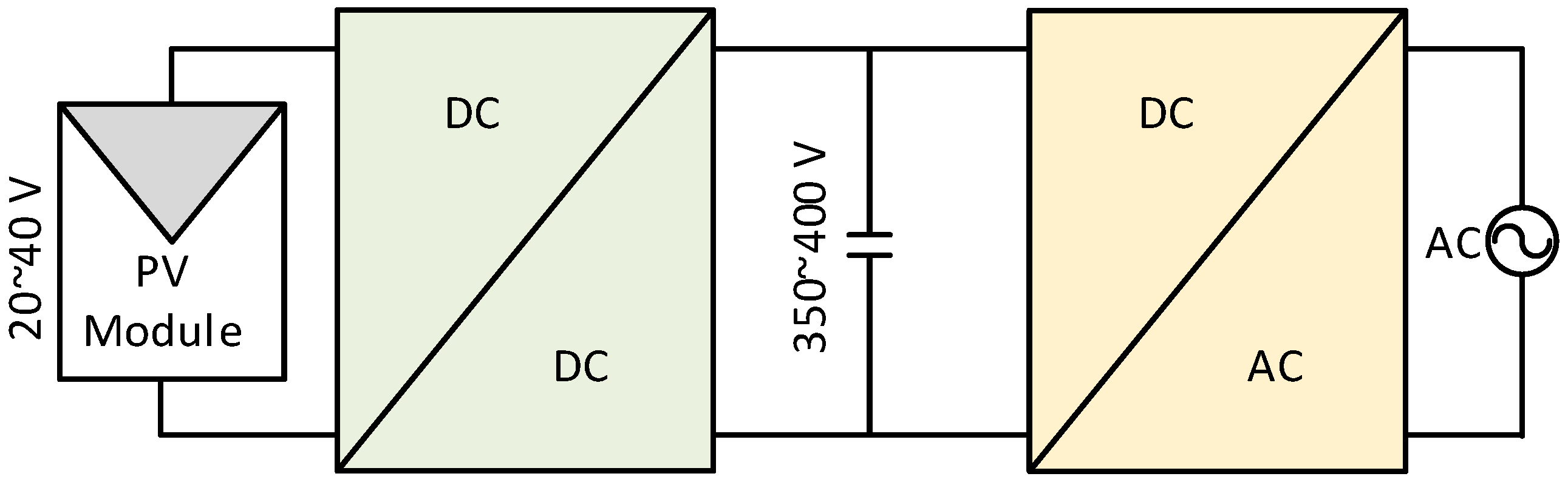
Currently, dc/dc converters are used in most industrial applications. However, for photovoltaic (PV) energy systems, a step-up dc/dc boost converter is mandatory to boost the low voltage to higher level to enable grid integration or supply power to an islanded load, see Figure 1. In most of the practical cases, the converter is configured to generate output voltage around 400 V, with input voltage only ranging from 18 to 50 V [1,2,3,4].
In ideal scenarios, the voltage gain of the classical boost converter is infinite. However, practically, its step-up ability is limited and restricted by the power device’s parasitic components, capacitance and inductance, and conduction losses caused by resistances and diode voltage drops. Another limitation for having such a high step-up ratio is that triggering the power switch during the high duty cycle may causes reverse recovery problems and magnetic saturation issues [5,6,7,8]. Several papers have been published in the literature, attempting to create boost converters with high gain and high efficiency [9,10,11,12,13,14,15,16,17]. Step-up dc/dc converters can be classified based on the inclusion of a transformer that is isolated vs. non-isolated. Topologies that include a transformer can provide high voltage-gain by controlling the turns ratio of the transformer. Moreover, transformers provide isolation between the output and input sides. Transformerless topologies are competitive in terms of cost, weight, and design simplicity [15].
Topology presented in [17], which is based on cascading boost converters, is able to achieve higher voltage gain without an extreme duty cycle as compared to the classical boost converter; however, its switching devices are under high voltage/current stress.
Another possible solution for providing a higher voltage gain is the use of switched inductors/capacitors [18,19,20,21,22]. A switched inductor converter has a voltage gain double of that reported for the classical boost converter; however, its semiconductors are under high voltage stress.
In some papers, voltage lift methodology is applied [23,24,25] in order to achieve high voltage-gain, as well as reduce voltage/current stress on the switches. However, multiple diodes and capacitors are required when the conversion ratio is high.
Isolated topologies, such as coupled inductors and flyback converters, use the turns ratio, in addition to the duty cycle, to control the converter voltage gain. As the required step-up ratio is performed at moderate duty cycle, the overall efficiency is increased. However, in topologies such as the flyback converter, voltage spikes on the active switch appear due to the discharging energy of leakage inductance. Increasing dissipations are the inevitable result of the discharging energy of leakage inductance on the active switch [25,26]. Different solutions for such problems exist such as the employment of active clamp circuits (considered a costly solution) and passive clamp circuits [26,27].
Switched capacitor converters are used to provide boosting ability without any magnetic components [28,29,30,31]. Hard switching switched capacitor boost converters suffer from low efficiency, less than 75%, as reported in [32]. Adding a resonance inductor improves the switched capacitor performance [32,33]. The boosting range is still somewhat limited compared to converters with inductors, the duty cycle of which can be varied for a wide range of boosting.
In certain applications, the PV module is connected directly to its dc-dc converter; in this case, input voltage would be in the range of 33 V to 45 V; hence, a high step-up ability is mandatory. One of the main functions of the dc-dc converter is to elevate module voltage from 33~50 V to 400~700 V. Hence, a high step-up ability is required. In this paper, a new dc/dc converter with high step-up ability is proposed. The proposed converter is well suited for different applications, such as photovoltaic (PV) systems. The proposed topology has some distinct advantages, including a high step-up capability, low voltage-stress on the active devices, and moderate efficiency.
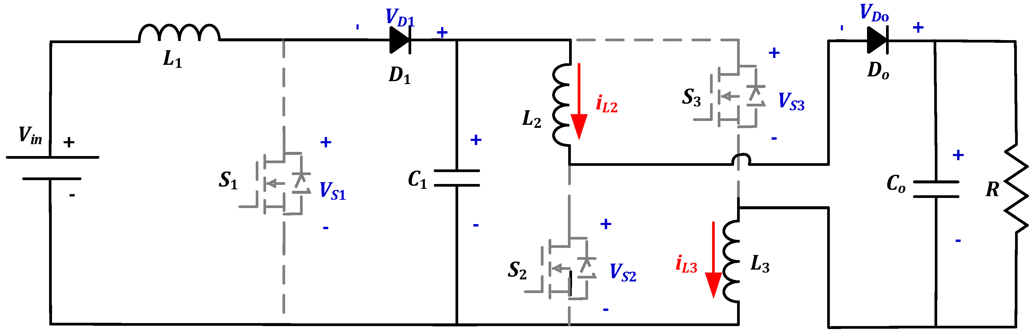
2. Proposed High Step-Up Converter
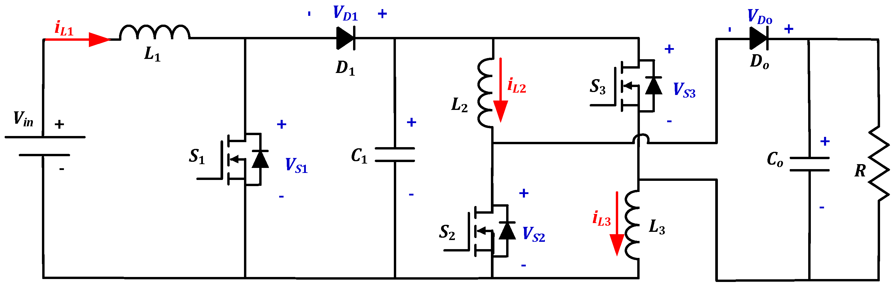
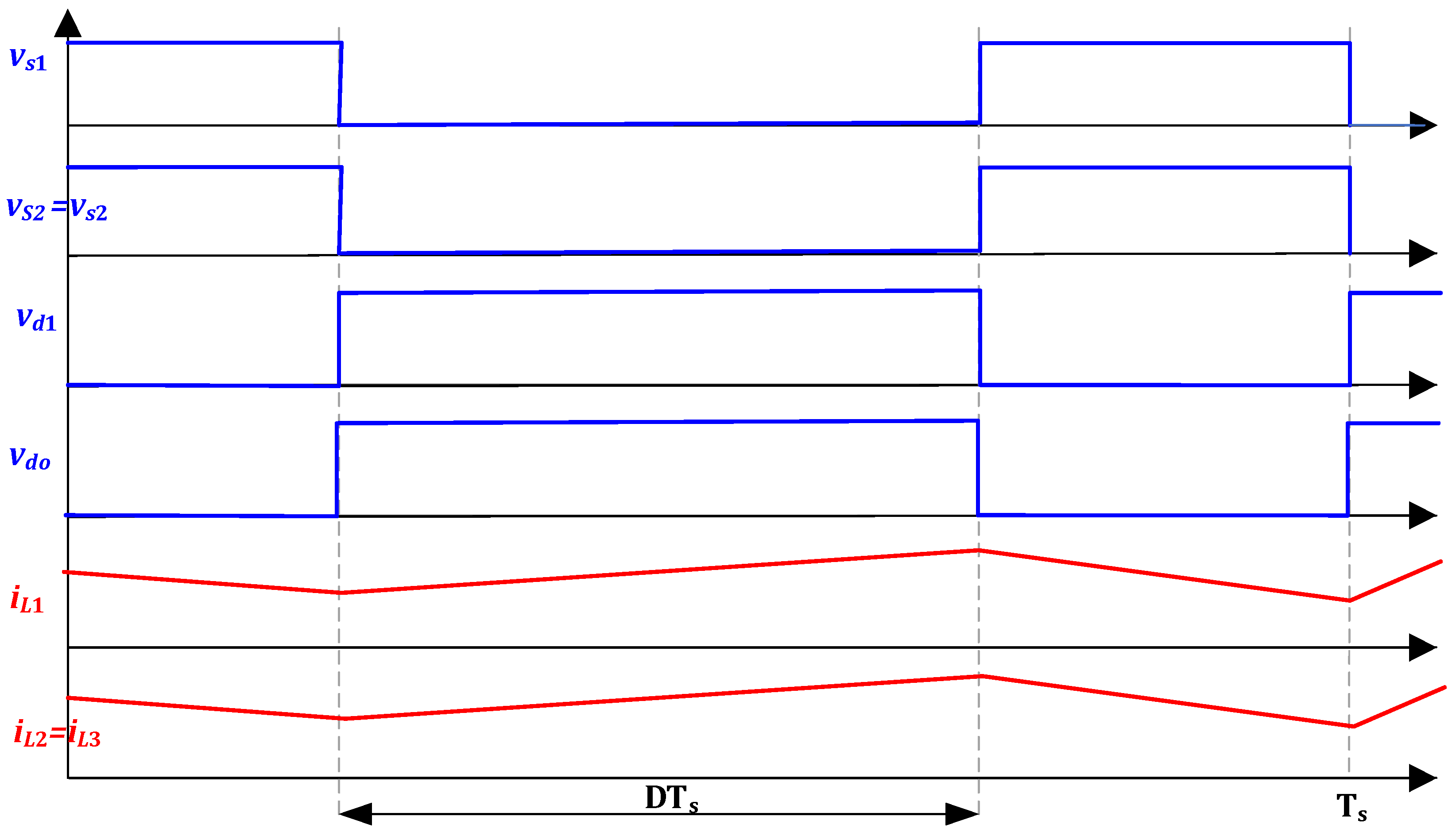
The configuration of the proposed converter is depicted in Figure 2. It consists of two diodes, three inductors, two capacitors, and three switches. The three switches are triggered on and off simultaneously. The two-diodes are operate in a complementary manner to the switches in order to provide a free path for the inductor current. Inductors charge in parallel when the switches are turned on and discharge their energy to the output load once switches are turned off. In the upcoming analysis, the small-ripple approximation is used. The converter is designed to operate in the continuous conduction mode (CCM). The parameters are assumed to be ideal for the upcoming analysis in order to facilitate the analysis of the converter. A graph of the ideal key waveforms of the circuit devices is shown in Figure 3. The two possible operating modes of the converter are discussed as follows:
2.1. Mode I
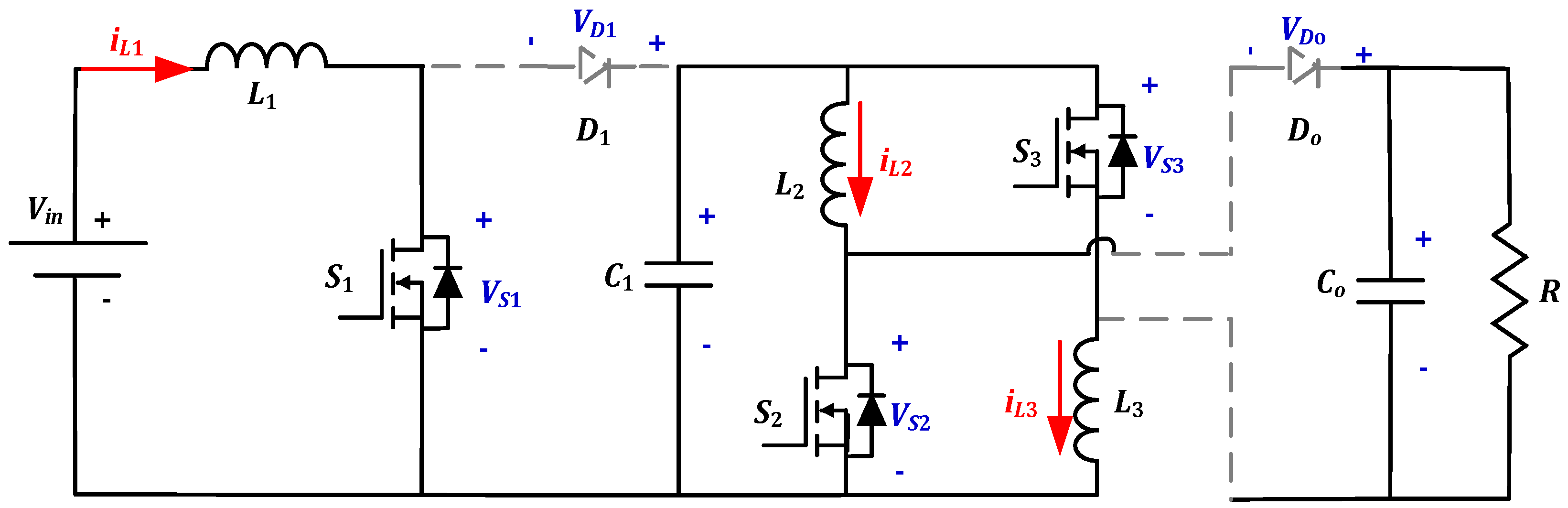
This mode is activated once the switches are turned on, and the depiction of this mode is illustrated in Figure 4. The three switches are turned on simultaneously. In this mode, inductor L1 is energized from the input dc-source, while inductors L2 and L3 are energized from capacitor C1. Diodes D1 and Do are reversely biased. Output capacitor Co releases its energy to the load side. The characteristic equations that describe this mode of operation are as follows:
where Vin, Vo, Vc1, D, R, VL1, VL2, ico, iL1, and iL2 are denoted to input voltage, output voltage, capacitor C1 voltage, duty cycle, load resistance, inductor L1 voltage, inductor L2 voltage, capacitor Co current, inductor L1 current and inductor L2 current, respectively.
2.2. Mode II
This mode is activated once the switches are turned off, and the depiction of this mode is illustrated in Figure 5. The three switches are turned off at the same time. In this mode, inductor L1 is discharging its energy into capacitor C1, while inductors L2 and L3 are discharging their energy into output load and output capacitor Co. In order to maintain a continuous path for the inductor currents, diodes D1 and Do work as freewheeling diodes when they are turned on. The characteristic equations that describe this mode of operation are as follows:
The steady state voltage of capacitor C1 is obtained from (1) and (2).
Equation (3) represents the relationship between the voltage across capacitor C1 and input/output voltages. The voltage gain of the converter is given by Equation (4).
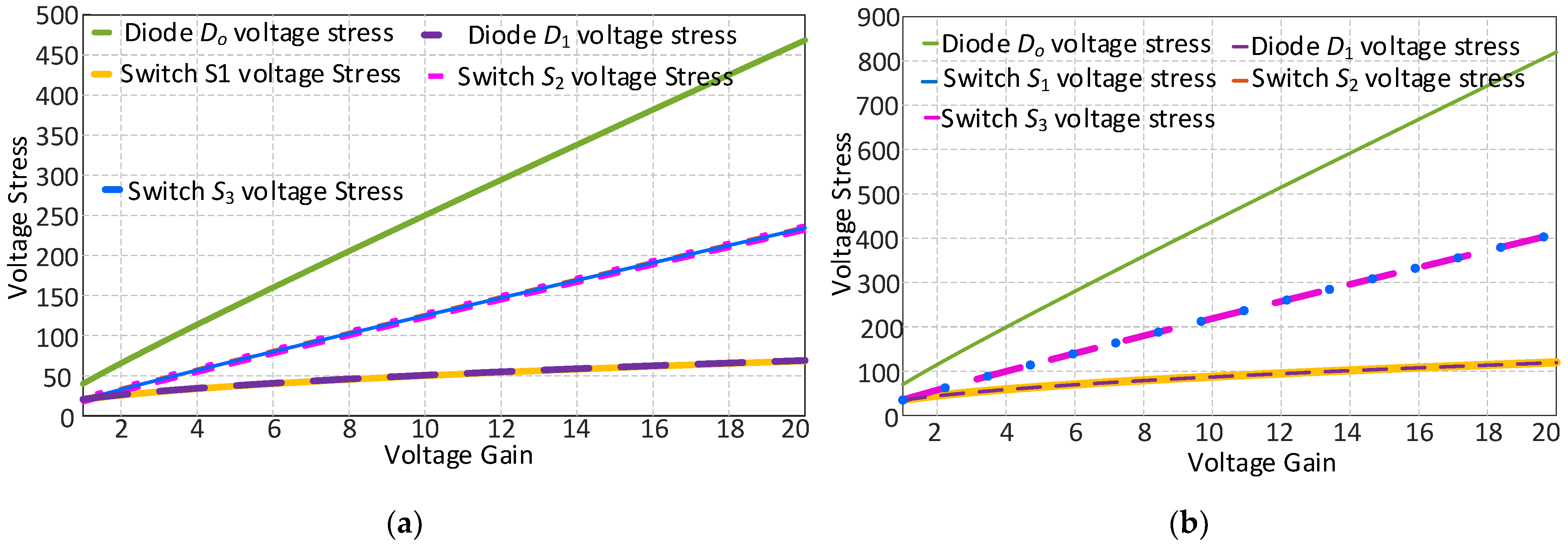
The voltage and current stresses of each component are depicted in Table 1 and Table 2, respectively. All components have a voltage stress lower than the output voltage. This is a distinct advantage of this topology. It enables us to select the devices with low ratings, thus improving the overall efficiency of the system.
Figure 6 is the depiction of the device voltage stress as a function of the converter voltage gain with a fixed input voltage. The switch S1 and diode D1 are under the same voltage stress, while the output diode Do is the component under the highest voltage stress.
The design and selection of converter parameters, such as inductor and capacitor values, are based on the amount of ripple allowed on each element. The design of the proposed circuit parameters are illustrated in the following sections.
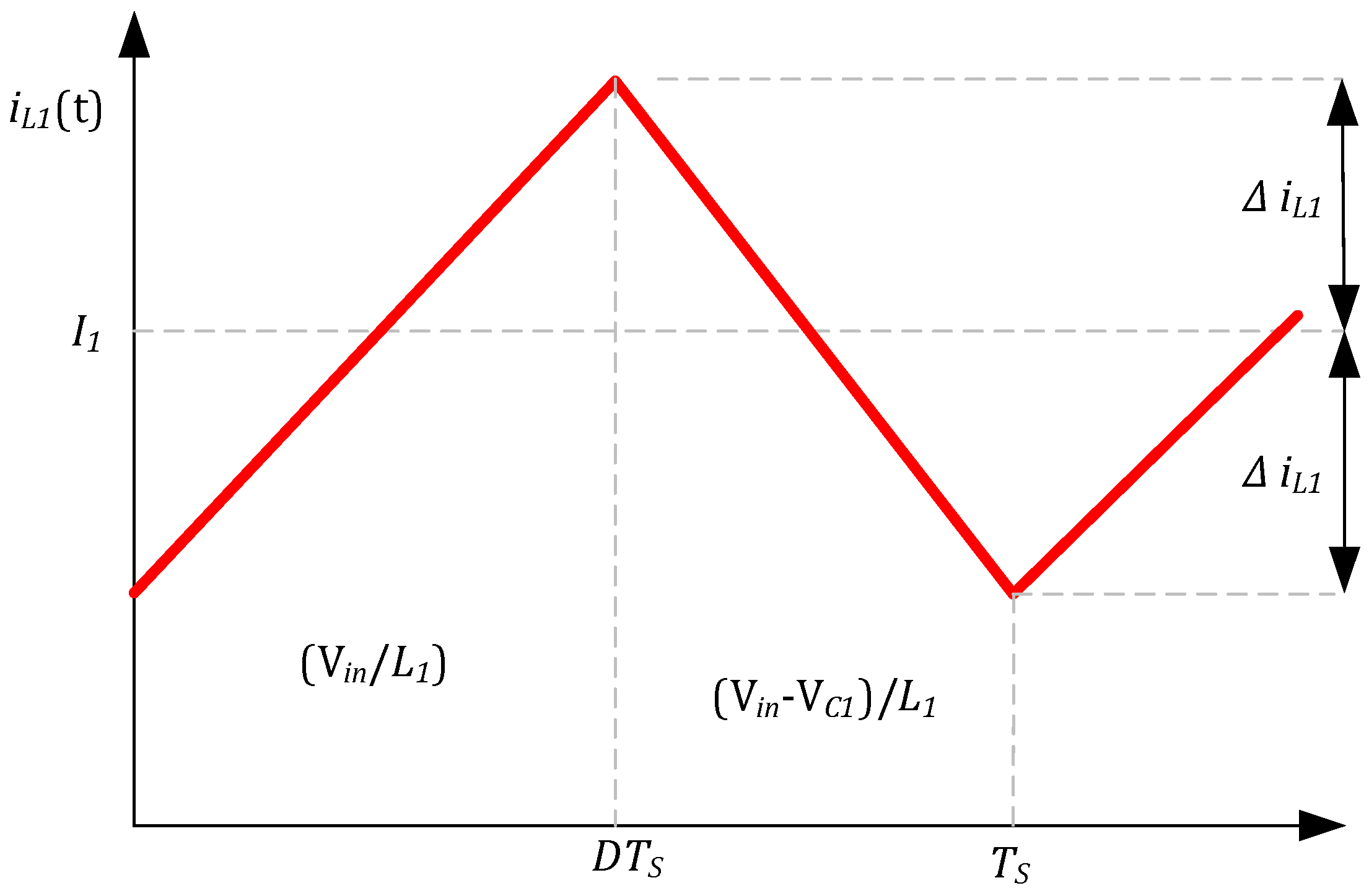
2.3. Inductor L1 Design
The inductor L1 current is shown in Figure 7. The average value of the inductor L1 current is defined as I1 and the difference between the inductor peak and the average current is Δ.
Considering the first interval of the switching cycle, the ripple of inductor L1 is given by
As Equation (6) describes, the inductance of L1 depends on the input voltage Vin, duty cycle D, sample time TS, and inductor current ripple .
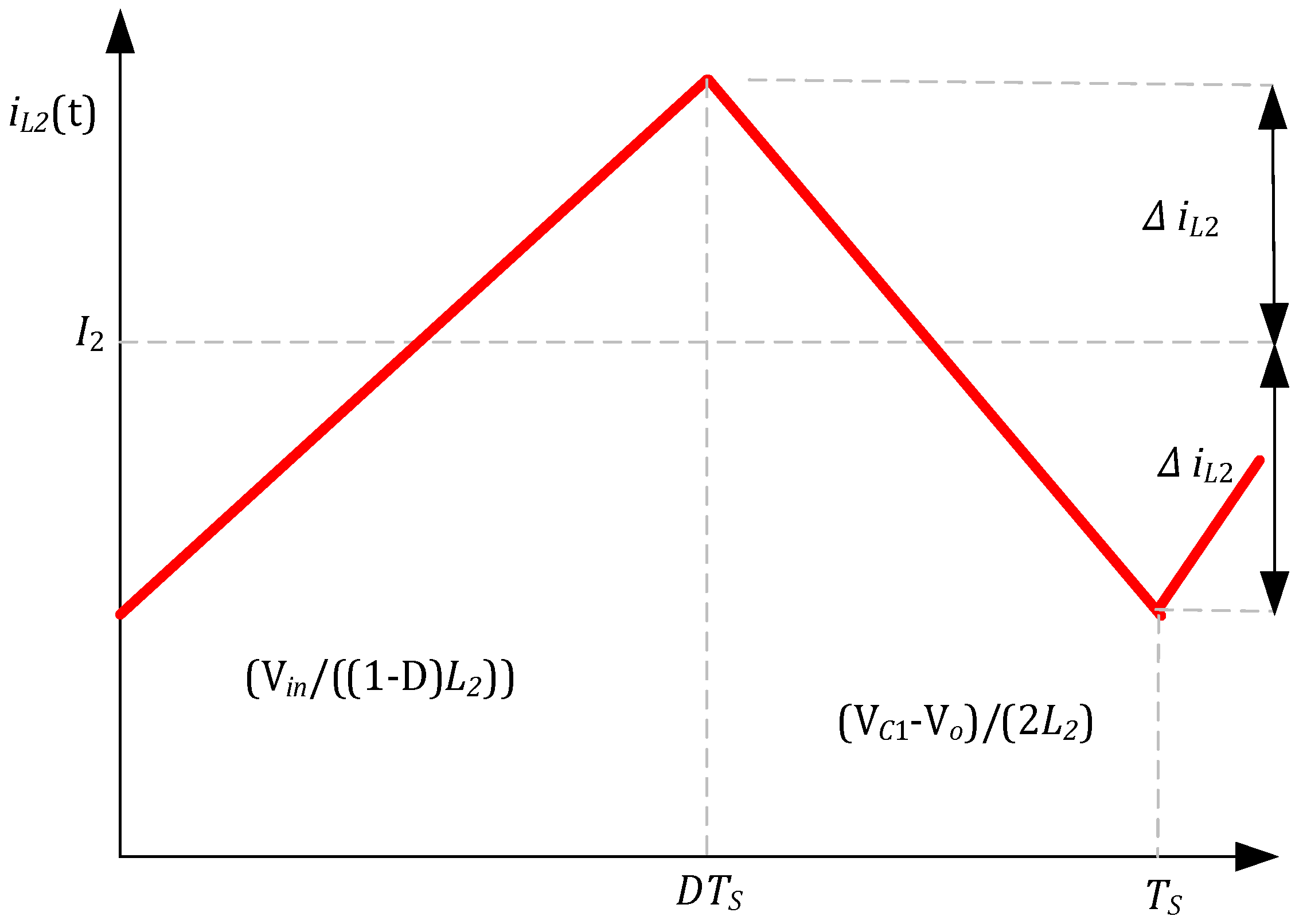
2.4. Inductor L2 and L3 Design
The inductor L2, which is similar to L3, current is shown in Figure 8. The average value of the inductor L2 current is defined as I2 and the difference between the inductor peak and the average current is Δ. Considering the first interval of the switching cycle, the ripple of inductor L2 is given by
As Equation (8) describes, the inductance of inductors L2 and L3 depend on the input voltage Vin, duty cycle D, sample time Ts, and the inductor current ripple ΔiL2.
2.5. Output Capacitor Co-Design
The output voltage ripple of the converter is limited by the amount of ripple permitted on the capacitor Co voltage. Consequently, capacitor Co should be designed to ensure that the converter output voltage exhibits ripple within the permitted range.
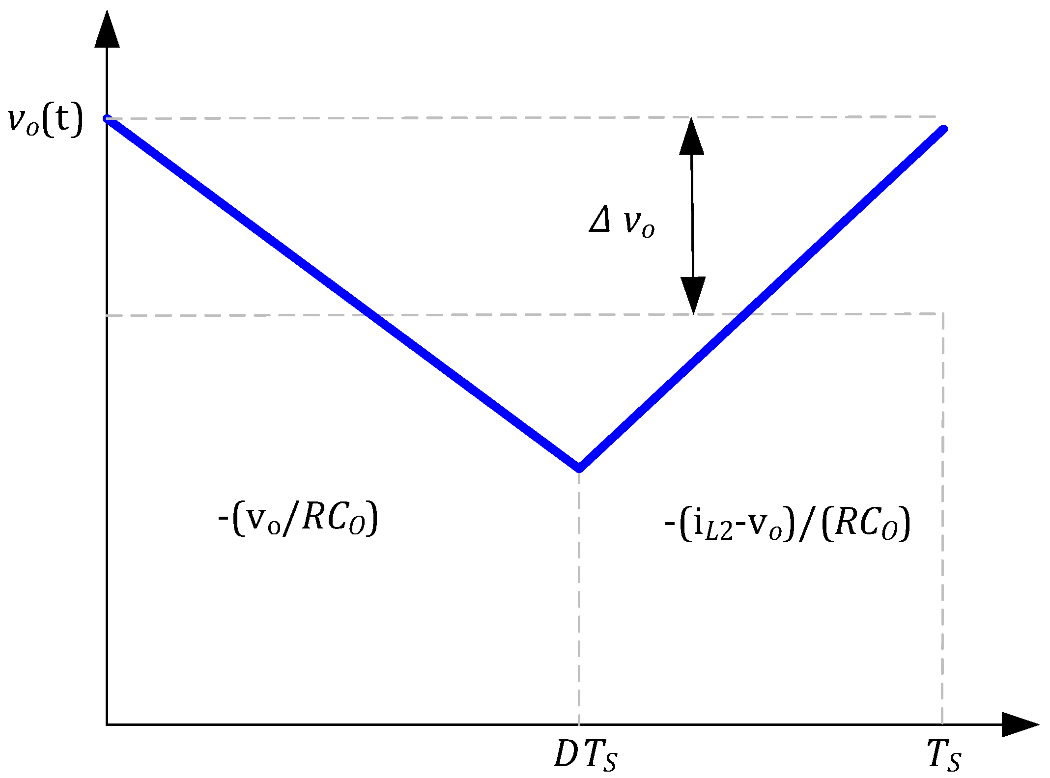
The capacitor Co voltage is expressed in Figure 9, where Vo is the capacitor voltage average value and the difference between the capacitor peak and the average voltage is Δvo. Considering the first interval of the switching cycle, the ripple of capacitor Co is given by
As can be seen from Equation (10), the value of capacitor Co depends on the output voltage Vo, duty cycle D, sample time TS, and the capacitor voltage ripple Δvo.
2.6. Capacitor C1 Design
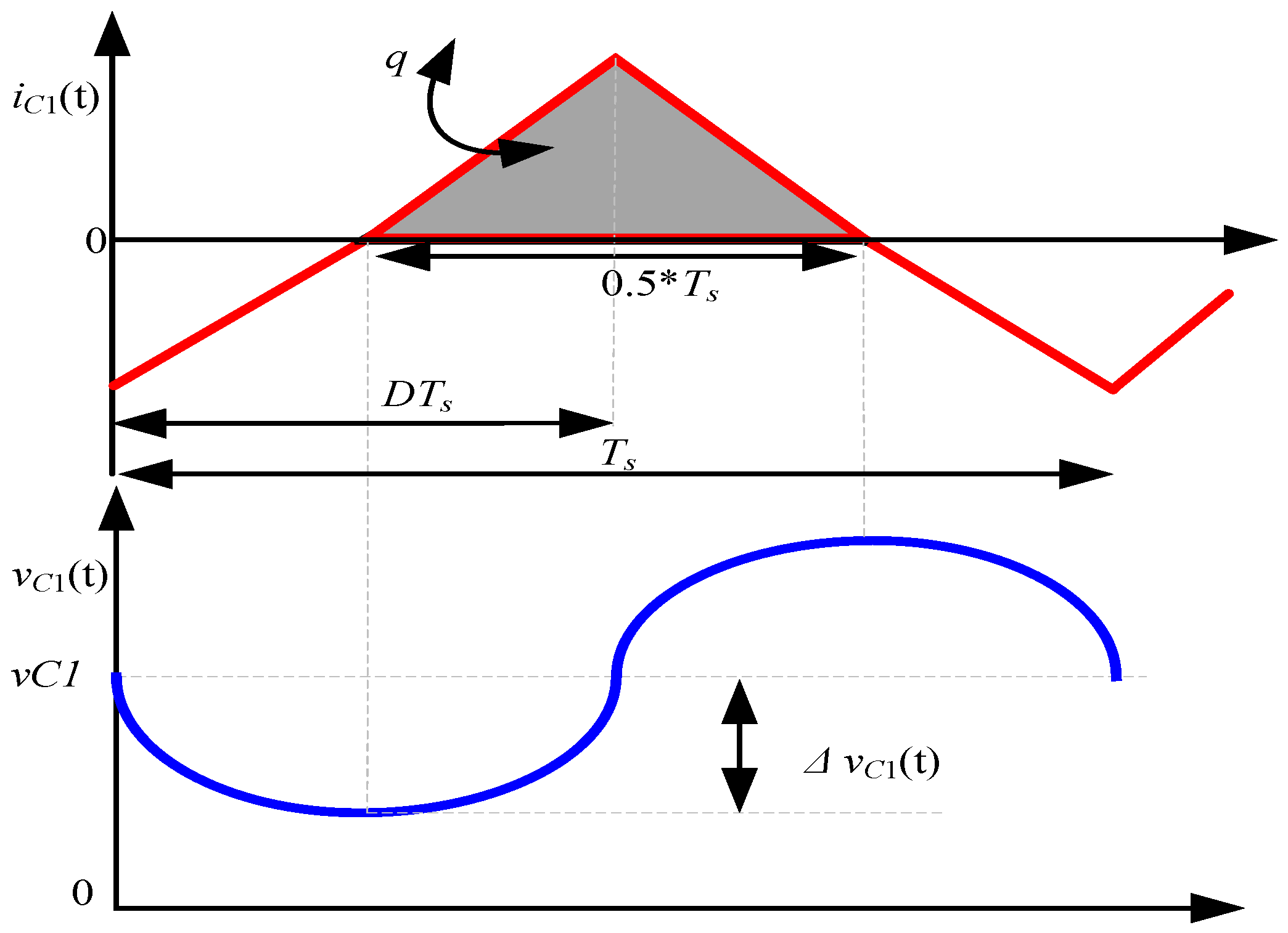
The design of capacitor C1 is not straightforward; similar to capacitor Co, its current is equal to the inductor L1 current, but without the dc components (see Figure 10). As seen in Figure 9, the capacitor C1 voltage reaches its maximum and minimum limits at the two zero crossing points of is current waveforms [34].
Let be the difference between the average and max value of the capacitor C1 voltage value; the relation between the total charge q and the peak-to-peak ripple of the capacitor C1 voltage is
The value of charge q is obtained by integrating the shaded area of the capacitor C1 current (see Figure 9), and due to the symmetry of the capacitor, the current waveform q is given by:
Substitute Equation (12) into Equation (11) and a solution for the voltage ripple peak amplitude yields
Hence,
The capacitor C1 value depends on the inductor L1 current ripple, the sampling time, and the permitted ripple on the capacitor C1.
3. Results
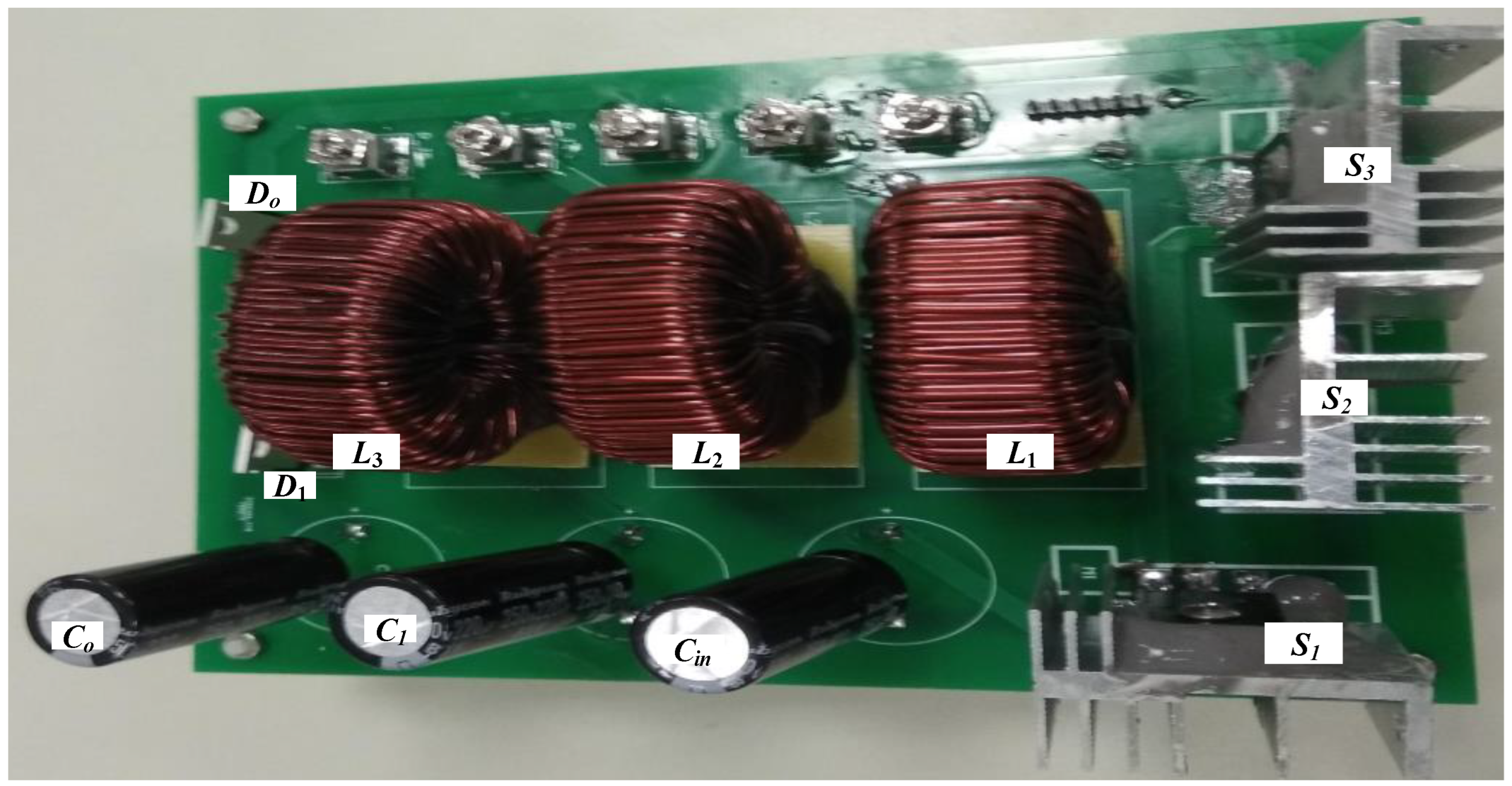
A testbench for the proposed converter was implemented in the laboratory to verify its operation and characteristics. The parameters used for implementing the proposed converter are given in Table 3. The developed prototype is illustrated in Figure 11.
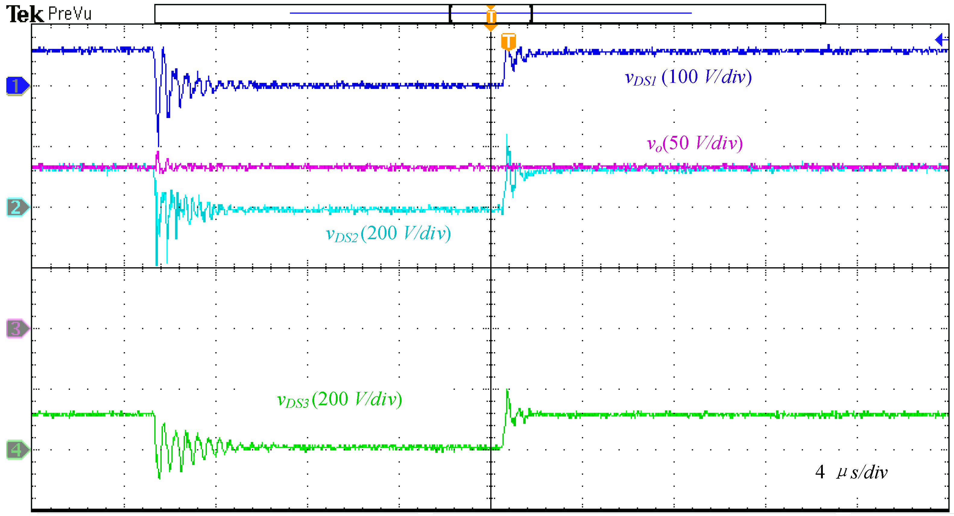
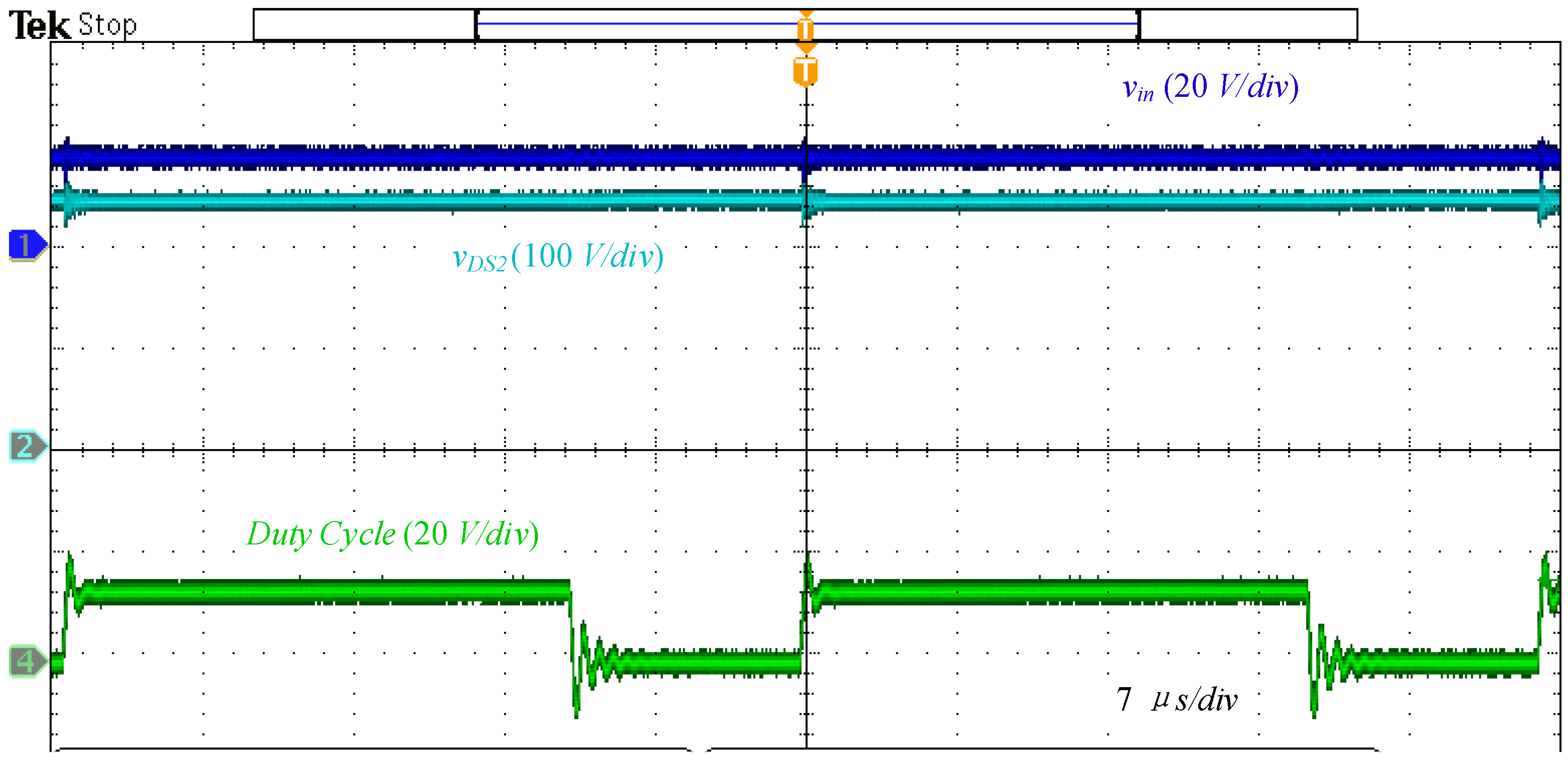
The three switches are triggered simultaneously to avoid any short circuits; hence, no deadtime is added to the controller. Switches S2 and S3 face similar voltage stress, while S1 encounters a different voltage stress (see Figure 12). Figure 12 is a case of study in which the duty cycle is set to 0.4, the input voltage is 35 V, and the measured output across the converter voltage is around 130 V.
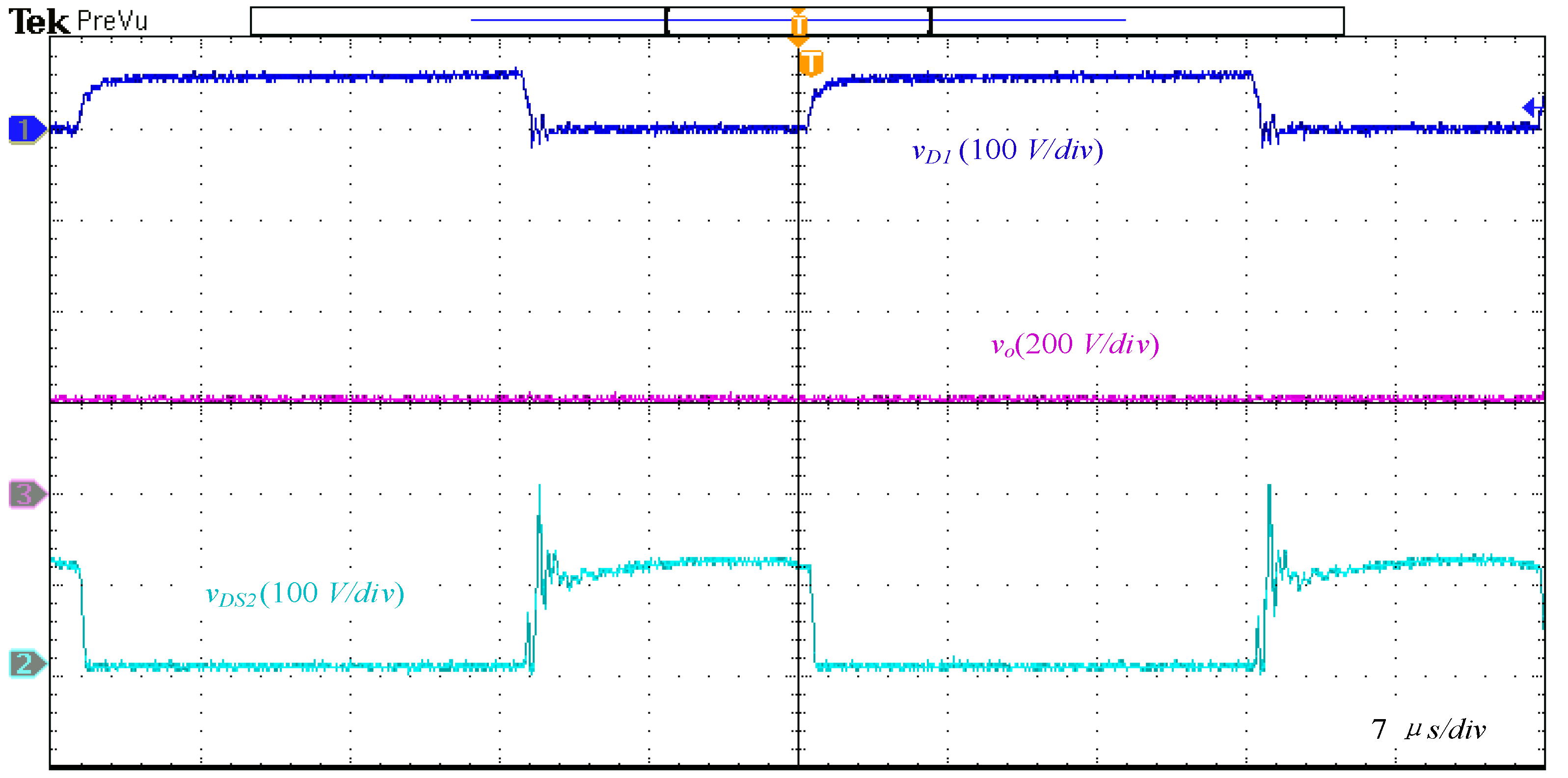
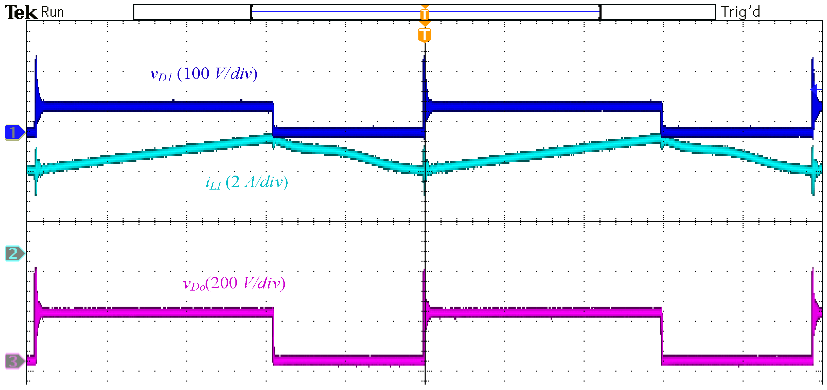
The circuit diodes D1 and Do operate as a freewheeling diodes, and both are on when the switches are off. The diode D1 reverse voltage is illustrated in Figure 13. Figure 13 shows a new case study, where the duty cycle is set to 0.6 with 20 V input voltage, and the output voltage is around 200 V. The inductor L1 current is illustrated in Figure 14.
In the case study shown in Figure 15, the converter duty cycle is set to 0.6 with 20 V input voltage; the measured output voltage in this case is around 240 V.
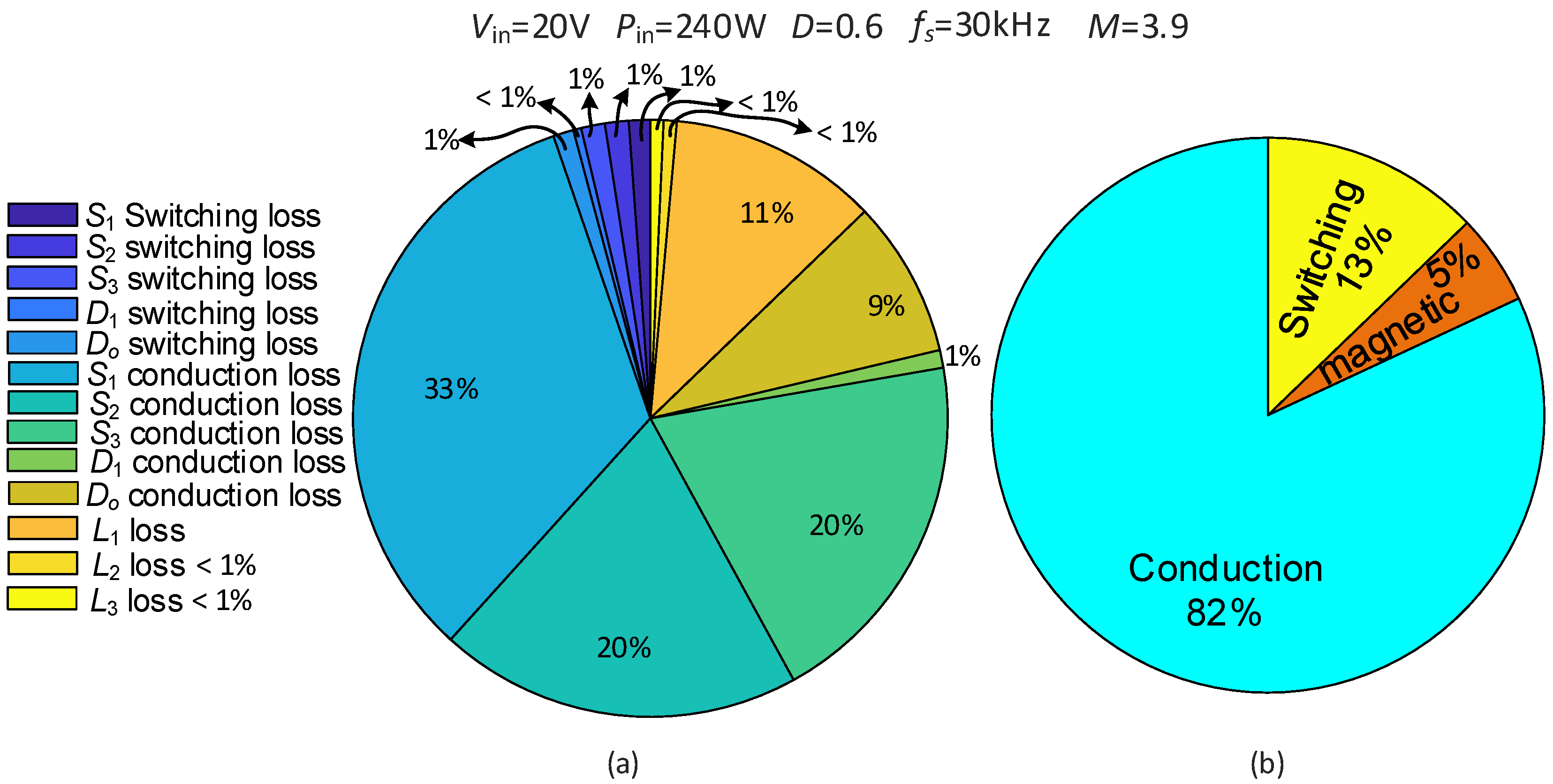
An analytical analysis for the converter losses is performed with the help of PSIM thermal modules. A case study is illustrated in Figure 16, where the input power, input voltage, switching frequency, voltage gain and duty cycle are set to 20 V, 240 W, 30 kHz, 3.9, and 0.6, respectively. As illustrated in the figure, the conduction losses are dominant. The switch S1 is the main source of conduction losses, while inductor L1 has the highest value of conduction loss compared to L2 and L3.
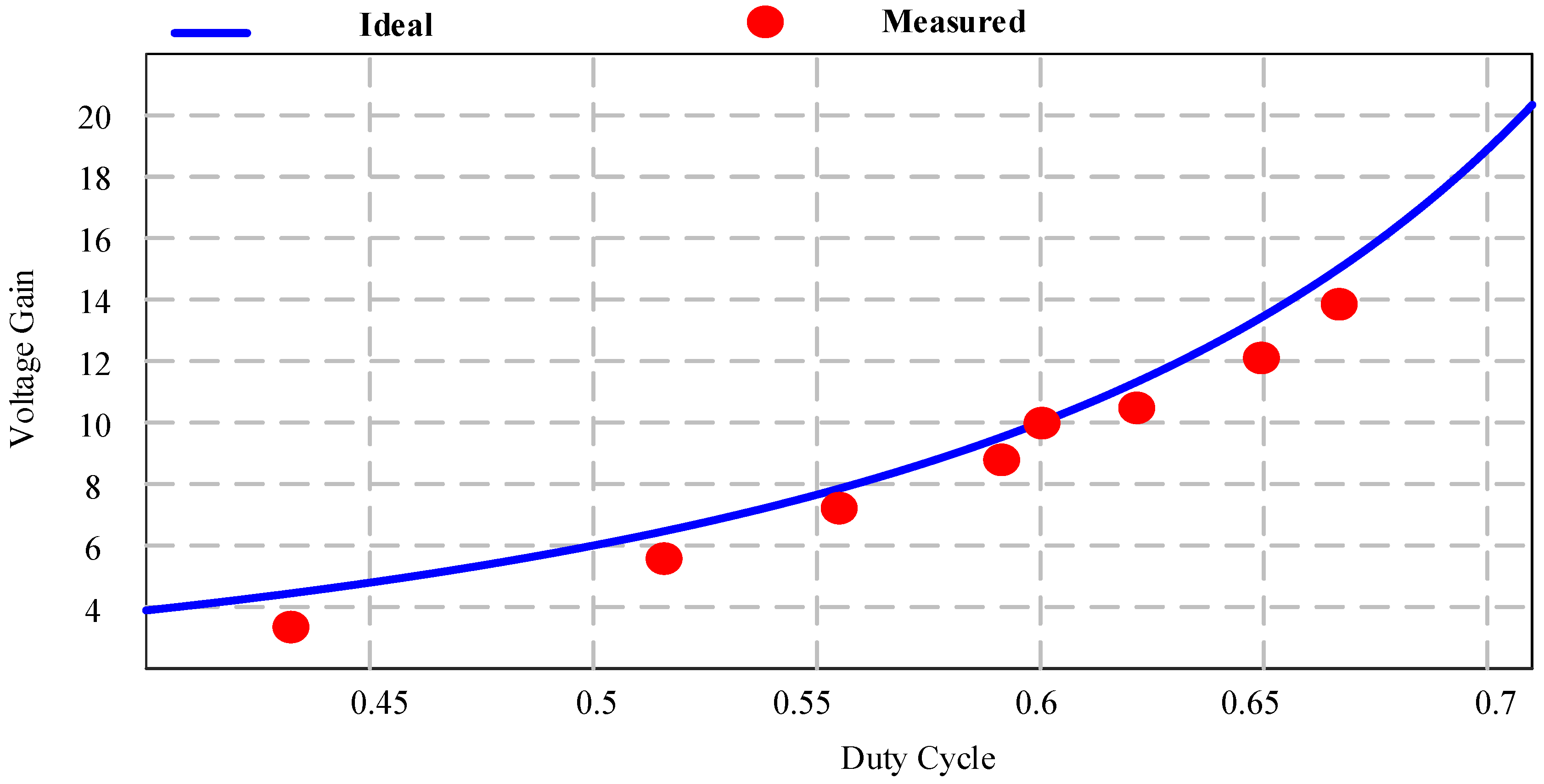
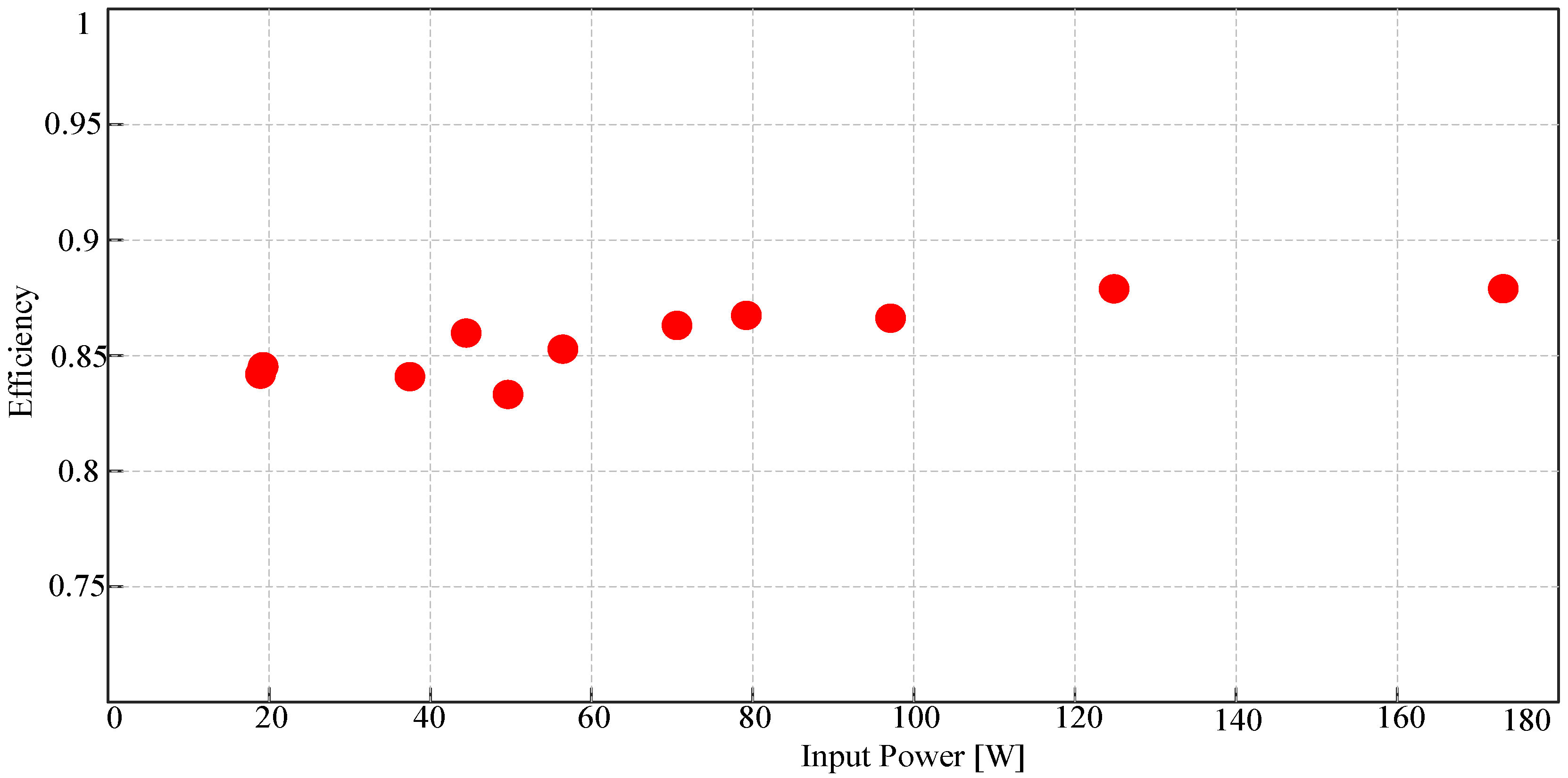
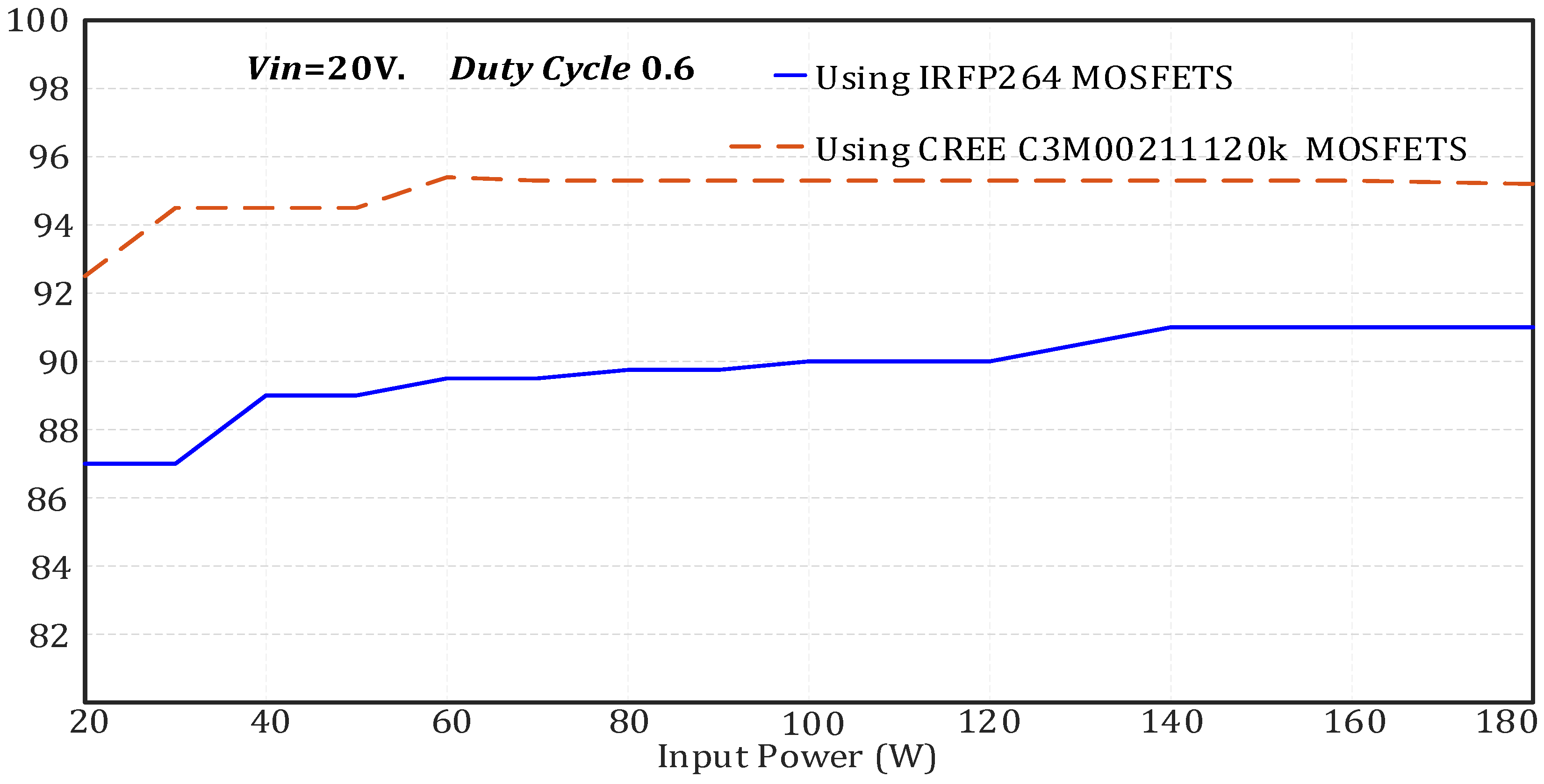
Figure 17 illustrates the relation between the calculated and measured converter voltage gain; the results are consistent and the slight differences are due to the effect of the losses on the converter voltage gain. Efficiency is a major factor in selecting a converter for a specific application, and achieving higher efficiency at a higher voltage gain is a desirable factor for some applications, such as for PV microconverters. Figure 18 is a depiction of the efficiency of the proposed converter, with the input voltage set to 20 V and the duty cycle set to 0.6; the voltage gain at this point is around 10 times that illustrated in Figure 13. Converter efficiency improves by increasing the input power. Efficiency at 175 W input power is around 88%, which is comparable compared to the results reported in the literature. The main sources for losses are the semiconductors. In Figure 19, two case studies are presented where the converter efficiency is measured using IRFP264 MOSFETs and CREE C3M00211120k. Utilizing silicon carbide switches improves the efficiency due to very low resistance, in a range of 21 mΩ, and very small switching losses. Nevertheless, this comes at a very high cost.
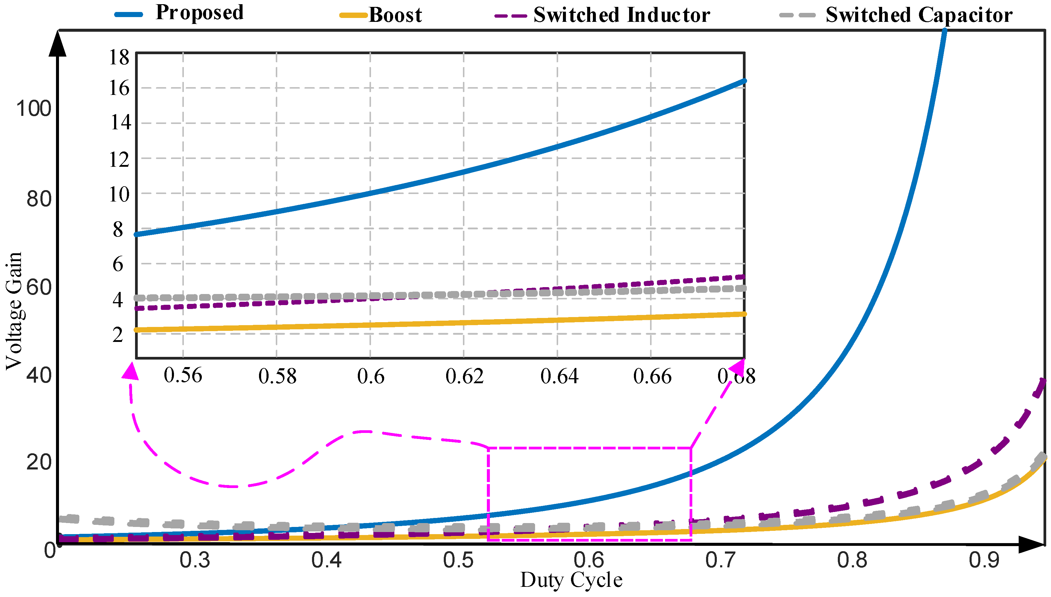
In the literature, several solutions have been presented for integrating PV systems into existing systems. Providing high step-up capability is a mandatory characteristic for any converter used in photovoltaic applications. Figure 20 provides a voltage gain comparison between the proposed topology and other transformerless topologies reported in the literature. The graph plots the voltage gain of all the converters with variable duty cycles. The traditional boost converter has the minimum boosting capability among all presented converters, while the proposed converter has the highest gain among the different topologies. Table 4 compares the different topologies with the proposed topology from the point of view of the number of active switches, number of diodes, and voltage stresses for each device. The proposed converter provides high voltage-gain, while at the same time, imposing small voltage stresses on the active devices. Such features make the proposed converter a very good candidate for PV microconverter applications.
4. Conclusions
The purpose of this work was to develop a new dc/dc boost configuration with high voltage-gain capability for PV converters. The developed configuration consisted of three switches, two diodes, and three inductors. A theoretical analysis of the converter demonstrated its high voltage-gain, low voltage and current stress on its devices, and moderate efficiency. The experimental results obtained were consistent with the theoretical analysis of the converter. To support our results, a comparison with other topologies presented in the literature is provided.
Author Contributions
O.A.-R. designed and performed the simulations and obtained the results; O.A.-R., H.Y.A. and Z.M.A. analyzed the obtained results; O.A.-R. and Z.M.A. wrote the paper, which was further reviewed by H.Y.A. All authors have read and agreed to the published version of the manuscript.
Funding
The authors extend their appreciation to the Deputyship for Research & Innovation, Ministry of Education, Saudi Arabia, for funding this research work through project number (IF-PSAU-2021/01/18678).
Data Availability Statement
The data presented in this study are available on request from the corresponding author. The data are not publicly available due to their large size.
Acknowledgments
The authors extend their appreciation to the Deputyship for Research & Innovation, Ministry of Education, Saudi Arabia, for funding this research work through the project number (IF-PSAU-2021/01/18678).
Conflicts of Interest
The authors declare no conflict of interest.
References
- Abdel-Rahim, O.; Funato, H.; Haruna, J. A comprehensive study of three high gain dc-dc topologies based on cockcroft-walton voltage-multiplier for reduced power PV applications. IEEJ Trans. Electr. Electron. Eng. 2018, 13, 642–651. [Google Scholar] [CrossRef]
- Zaid, M.; Lin, C.-H.; Khan, S.; Ahmad, J.; Tariq, M.; Mahmood, A.; Sarwar, A.; Alamri, B.; Alahmadi, A. A Family of transformerless quadratic boost high gain dc-dc converters. Energies 2021, 14, 4372. [Google Scholar] [CrossRef]
- Barbosa, E.A.O.; Carvalho, M.R.S.D.; Rodrigues Limongi, L.; Cavalcanti, M.C.; Barbosa, E.J.; Azevedo, G.M.D.S. High-gain high-efficiency dc–dc converter with single-core parallel operation switched inductors and rectifier voltage multiplier cell. Energies 2021, 14, 4634. [Google Scholar] [CrossRef]
- Pereira, A.V.C.; Cavalcanti, M.C.; Azevedo, G.M.; Bradaschia, F.; Neto, R.C.; Carvalho, M.R.S.D. A novel single-switch high step-up dc–dc converter with three-winding coupled inductor. Energies 2021, 14, 6288. [Google Scholar] [CrossRef]
- Li, W.; He, X. Review of nonisolated high-step-up DC/DC converters in photovoltaic grid-connected applications. IEEE Trans. Ind. Electron. 2011, 58, 1239–1250. [Google Scholar] [CrossRef]
- Souza, L.C.; Morais, D.C.; Silva, L.D.S.D.C.E.; Seixas, F.J.M.D.; Arenas, L.D.O. DC-DC 3SSC-a-based boost converter: Analysis, design, and experimental validation. Energies 2021, 14, 6771. [Google Scholar] [CrossRef]
- Gholizadeh, H.; Gorji, S.A.; Afjei, E.; Sera, D. Design and implementation of a new cuk-based step-up DC–DC converter. Energies 2021, 14, 6975. [Google Scholar] [CrossRef]
- Chub, A.; Vinnikov, D.; Blaabjerg, F.; Peng, F.Z. A review of galvanically isolated impedance-source DC-DC converters. IEEE Trans. Power Electron. 2016, 31, 2808–2828. [Google Scholar] [CrossRef]
- Abdel-Rahim, O.; Wang, H. A new high gain DC-DC converter with model-predictive-control based MPPT technique for photovoltaic systems. CPSS Trans. Power Electron. Appl. 2020, 5, 191–200. [Google Scholar] [CrossRef]
- Arango, E.; Ramos-Paja, C.A.; Calvente, J.; Giral, R.; Serna-Garces, S.I. Asymmetrical interleaved dc/dc switching converters for photovoltaic and fuel cell applications—Part 2: Control-oriented models. Energies 2013, 6, 5570–5596. [Google Scholar] [CrossRef]
- Abdel-Rahim, O.; Chub, A.; Blinov, A.; Vinnikov, D. New high-gain non-inverting buck-boost converter. In Proceedings of the IECON 2021–47th Annual Conference of the IEEE Industrial Electronics Society, Toronto, ON, Canada, 13 October 2021; pp. 1–6. [Google Scholar]
- Ojeda-Rodríguez, Á.; González-Vizuete, P.; Bernal-Méndez, J.; Martín-Prats, M.A. A survey on bidirectional dc/dc power converter topologies for the future hybrid and all electric aircrafts. Energies 2020, 13, 4883. [Google Scholar] [CrossRef]
- De Souza, A.F.; Tofoli, F.L.; Ribeiro, E.R. Switched capacitor dc-dc converters: A survey on the main topologies, design characteristics, and applications. Energies 2021, 14, 2231. [Google Scholar] [CrossRef]
- Forouzesh, M.; Siwakoti, Y.P.; Gorji, S.A.; Blaabjerg, F.; Lehman, B. Step-up DC-DC converters: A comprehensive review of voltage-boosting techniques, topologies, and applications. IEEE Trans. Power Electron. 2017, 32, 9143–9178. [Google Scholar] [CrossRef]
- Andrade, A.M.S.S.; Martins, M.L.D.S. Quadratic-boost with stacked zeta converter for high voltage gain applications. IEEE J. Emerg. Sel. Top. Power Electron. 2017, 5, 1787–1796. [Google Scholar] [CrossRef]
- Ai, J.; Lin, M. Ultralarge gain step-up coupled-inductor dc-dc converter with an asymmetric voltage multiplier network for a sustainable energy system. IEEE Trans. Power Electron. 2017, 32, 6896–6903. [Google Scholar] [CrossRef]
- Vighetti, S.; Ferrieux, J.P.; Lembeye, Y. Optimization and design of a cascaded DC/DC converter devoted to grid-connected photovoltaic systems. IEEE Trans. Power Electron. 2012, 27, 2018–2027. [Google Scholar] [CrossRef]
- Zhang, Y.; Gao, Y.; Zhou, L.; Sumner, M. A switched-capacitor bidirectional dc-dc converter with wide voltage gain range for electric vehicles with hybrid energy sources. IEEE Trans. Power Electron. 2018, 33, 9459–9469. [Google Scholar] [CrossRef]
- Ballo, A.; Grasso, A.D.; Palumbo, G.; Tanzawa, T. Linear distribution of capacitance in Dickson charge pumps to reduce rise time. Int. J. Circ. Theor. Appl. 2020, 48, 555–566. [Google Scholar] [CrossRef]
- Ballo, A.; Grasso, A.D.; Palumbo, G. A simple and effective design strategy to increase power conversion efficiency of linear charge pumps. Int. J. Circ. Theor. Appl. 2020, 48, 157–161. [Google Scholar] [CrossRef]
- Ahmed, M.E.; Orabi, M.; AbdelRahim, O.M. Two-stage micro-grid inverter with high-voltage gain for photovoltaic applications. IET Power Electron. 2013, 6, 1812–1821. [Google Scholar] [CrossRef]
- Axelrod, B.; Berkovich, Y.; Ioinovici, A. Switched-capacitor/switched-inductor structures for getting transformerless hybrid DC–DC pwm converters. IEEE Trans. Circuits Syst. 2008, 55, 687–696. [Google Scholar] [CrossRef]
- Young, C.-M.; Chen, M.-H.; Chang, T.-A.; Ko, C.-C.; Jen, K.-K. Cascade Cockcroft–Walton Voltage Multiplier Applied to Transformerless High Step-Up DC–DC Converter. IEEE Trans. Ind. Electron. 2013, 60, 523–537. [Google Scholar] [CrossRef]
- Andrade, A.M.S.S.; Hey, H.L.; Schuch, L.; da Silva Martins, M.L. Comparative Evaluation of Single Switch High-Voltage Step-Up Topologies Based on Boost and Zeta PWM Cells. IEEE Trans. Ind. Electron. 2018, 65, 2322–2334. [Google Scholar] [CrossRef]
- Li, W.; Xiang, X.; Li, C.; Li, W.; He, X. Interleaved high step-up ZVT converter with built-in transformer voltage doubler cell for distributed PV generation system. IEEE Trans. Power Electron. 2013, 28, 300–313. [Google Scholar] [CrossRef]
- Liu, H.; Li, F. A novel high step-up converter with a quasi-active switched-inductor structure for renewable energy systems. IEEE Trans. Power Electron. 2016, 31, 5030–5039. [Google Scholar] [CrossRef]
- De Paula, W.J.; Júnior, D.D.O.; Pereira, D.D.; Tofoli, F.L. Survey on non-isolated high-voltage step-up dc–dc topologies based on the boost converter. IET Power Electron. 2015, 8, 2044–2057. [Google Scholar]
- Stauth, J.T.; Seeman, M.D.; Kesarwani, K. Resonant switched-capacitor converters for sub-module distributed photovoltaic power management. IEEE Trans. Power Electron. 2013, 28, 1189–1198. [Google Scholar] [CrossRef]
- Waradzyn, Z.; Stala, R.; Mondzik, A.; Penczek, A.; Skala, A.; Pirog, S. Efficiency Analysis of MOSFET-Based Air-Choke Resonant DC–DC Step-Up Switched-Capacitor Voltage Multipliers. IEEE Trans. Ind. Electron. 2017, 64, 8728–8738. [Google Scholar] [CrossRef]
- Cervera, A.; Evzelman, M.; Peretz, M.M.; Ben-Yaakov, S. A high-efficiency resonant switched capacitor converter with continuous conversion ratio. IEEE Trans. Power Electron. 2015, 30, 1373–1382. [Google Scholar] [CrossRef]
- Stala, R.; Waradzyn, Z.; Mondzik, A.; Penczek, A.; Skała, A. DC–DC high step-up converter with low count of switches based on resonant switched-capacitor topology. In Proceedings of the 2019 21st European Conference on Power Electronics and Applications (EPE’19 ECCE Europe), Genova, Italy, 2–5 September 2019; pp. P.1–P.10. [Google Scholar]
- Shoyama, M.; Naka, T.; Ninomiya, T. Resonant switched capacitor converter with high efficiency. In Proceedings of the 2004 IEEE 35th Annual Power Electronics Specialists Conference 2004, Aachen, Germany, 20–25 June 2004; Volume 5, pp. 3780–3786. [Google Scholar] [CrossRef]
- Kesarwani, K.; Sangwan, R.; Stauth, J.T. Resonant-switched capacitor converters for chip-scale power delivery: Design and implementation. IEEE Trans. Power Electron. 2015, 30, 6966–6977. [Google Scholar] [CrossRef]
- Erickson, R.W.; Maksimovic, D. Fundamentals of Power Electronics; Wiley: Hoboken, NJ, USA, 2013. [Google Scholar]
- Nguyen, M.; Duong, T.; Lim, Y. Switched-Capacitor-Based Dual-Switch High-Boost DC–DC Converter. IEEE Trans. Power Electron. 2018, 33, 4181–4189. [Google Scholar] [CrossRef]
- Ardi, H.; Ajami, A.; Kardan, F.; Avilagh, S.N. Analysis and implementation of a nonisolated bidirectional DC-DC converter with high voltage gain. IEEE Trans. Ind. Electron. 2016, 63, 4878–4888. [Google Scholar]
- Chen, M.; Hu, J.; Li, K.; Ioinovici, A. A new switched-capacitor based hybrid converter with large step-up DC gain and low voltage on its semiconductors. In Proceedings of the 2016 IEEE International Symposium on Circuits and Systems (ISCAS), Montréal, QC, Canada, 22–25 May 2016; pp. 1190–1193. [Google Scholar] [CrossRef]
- Ahmad, J.; Zaid, M.; Sarwar, A.; Lin, C.-H.; Asim, M.; Yadav, R.K.; Tariq, M.; Satpathi, K.; Alamri, B. A New High-Gain DC-DC Converter with Continuous Input Current for DC Microgrid Applications. Energies 2021, 14, 2629. [Google Scholar] [CrossRef]
Figure 1.
Two stage PV microinverter.

Figure 2.
The proposed configuration.

Figure 3.
The ideal key waveforms of the converter.

Figure 4.
The configuration of mode I.

Figure 5.
The configuration of mode II.

Figure 6.
The component voltage stress vs. voltage gain at an input voltage of (a) 20 V; (b) 35 V.

Figure 7.
The inductor L1 current.

Figure 8.
The inductors L2 and L3 currents.

Figure 9.
The capacitor Co output voltage.

Figure 10.
The capacitor C1 current and voltage.

Figure 11.
A photo of the hardware.

Figure 12.
The output voltage, switch S1 drain source voltage, S2 drain source voltage, and S3 drain source voltage at an input voltage 20 V and a duty cycle of 0.4.
Figure 12.
The output voltage, switch S1 drain source voltage, S2 drain source voltage, and S3 drain source voltage at an input voltage 20 V and a duty cycle of 0.4.

Figure 13.
The output voltage, switch S2 drain source voltage, and diode D1 reverse voltage at an input voltage of 20 V and a duty cycle of 0.6.
Figure 13.
The output voltage, switch S2 drain source voltage, and diode D1 reverse voltage at an input voltage of 20 V and a duty cycle of 0.6.

Figure 14.
The inductor L1 current, diode D1 reverse voltage, and diode Do reverse voltage.

Figure 15.
A case of study where the duty cycle is set to 0.65, and the input voltage is 20 V.

Figure 16.
The switching and conduction losses distribution—(a) element losses distribution; (b) total losses distribution.
Figure 16.
The switching and conduction losses distribution—(a) element losses distribution; (b) total losses distribution.

Figure 17.
The ideal and measured voltage gain.

Figure 18.
The measured efficiency.

Figure 19.
The converter efficiency using IRFP264 MOSFET and C3M00211120k CREE MOSFET.

Figure 20.
The voltage gain comparison among different dc-dc step-up topologies.


Table 1.
The voltage stresses of the switching devices.
| Switching Device | Peak Voltage Stress |
|---|---|
| S1 | Vo ∗ (1 − D)/(1 + D) |
| S2 | Vo/(1 + D) |
| S3 | Vo/(1 + D) |
| D1 | Vo ∗ (1 − D)/(1 + D) |
| Do | 2 ∗ Vo/(1 + D) |
Table 2.
The current stresses of the switching devices.
| Switching Device | RMS Current Stress |
|---|---|
| S1 | Iin ∗ |
| S2 | (1 − D) ∗ ∗ Iin/2 |
| S3 | (1 − D) ∗ ∗ Iin/2 |
| Freewheeling Diodes | Average Current Stress |
| D1 | Iin ∗ (1 − D) |
| Do | (1 − D)2 ∗ Iin/2 |
Table 3.
The specification of the system parameters.
| Component | Description | Specification |
|---|---|---|
| Vin | Input voltage | 20–35 V |
| Vo | Output voltage | 100–350 |
| L1, L2, L3 | Input inductor | 3 mH |
| Cin | Input capacitor | 260 μF |
| C1 | Parallel capacitor | 260 μF |
| Co | Output capacitor | 260 μF |
| S1, S2 and S3 | Power MOSFET | IRFP264 |
| D1 | Power diode | BYV72EW-200 |
| Do | Output diode | BYV72EW-200 |
| FS | Switching frequency | 30 KHZ |
| Po | Rated output power | 175 W |
Table 4.
The comparison of Step-up Topologies.
| Topology | Boost | SL-Boost | SC-Boost | [35] | [36] | [37] | [38] | New | |
|---|---|---|---|---|---|---|---|---|---|
| No. Switches | 1 | 1 | 1 | 2 | 4 | 2 | 2 | 3 | |
| No. Diode | 1 | 4 | 3 | 4 | 0 | 6 | 2 | 2 | |
| Voltage Gain | |||||||||
| Switch Stress | S1 | Vo | Vo | Vo | |||||
| S2 | - | - | - | Vo | |||||
| S3 | - | - | - | - | Vo | - | - | ||
| S4 | - | - | - | - | Vo (1 − D) | - | - | - | |
| Diode Stress | D1 | - | Vin | - | - | ||||
| D2 | - | - | - | Vo + Vin | - | ||||
| D3 | - | - | - | - | - | ||||
| D5 | - | - | - | - | - | - | - | ||
| Do | Vo | Vo | Vo − Vin | - | - | ||||
| Passive component | L | 1 | 2 | 1 | 1 | 2 | 1 | 3 | |
| C | 1 | 1 | 3 | 3 | 2 | 5 | 2 | ||
Publisher’s Note: MDPI stays neutral with regard to jurisdictional claims in published maps and institutional affiliations. |
© 2022 by the authors. Licensee MDPI, Basel, Switzerland. This article is an open access article distributed under the terms and conditions of the Creative Commons Attribution (CC BY) license (https://creativecommons.org/licenses/by/4.0/).
Share and Cite
MDPI and ACS Style
Ahmed, H.Y.; Abdel-Rahim, O.; Ali, Z.M. New High-Gain Transformerless DC/DC Boost Converter System. Electronics 2022, 11, 734. https://doi.org/10.3390/electronics11050734
AMA Style
Ahmed HY, Abdel-Rahim O, Ali ZM. New High-Gain Transformerless DC/DC Boost Converter System. Electronics. 2022; 11(5):734. https://doi.org/10.3390/electronics11050734
Chicago/Turabian StyleAhmed, Hassan Yousif, Omar Abdel-Rahim, and Ziad M. Ali. 2022. "New High-Gain Transformerless DC/DC Boost Converter System" Electronics 11, no. 5: 734. https://doi.org/10.3390/electronics11050734
Note that from the first issue of 2016, this journal uses article numbers instead of page numbers. See further details here.