
Wideband mm-Wave Hemispherical Dielectric Resonator Antenna with Simple Alignment and Assembly Procedures

1
Communications Research Group, Department of Electronic and Electrical Engineering, The University of Sheffield, Mappin Street, Sheffield S1 3JD, UK
2
Electrical Engineering Department, Jouf University, Sakaka 72388, Saudi Arabia
*
Authors to whom correspondence should be addressed.
Electronics 2022, 11(18), 2917; https://doi.org/10.3390/electronics11182917
Submission received: 1 August 2022
/
Revised: 7 September 2022
/
Accepted: 12 September 2022
/
Published: 14 September 2022
(This article belongs to the Special Issue Antennas in the 5G System, Volume II)
Abstract
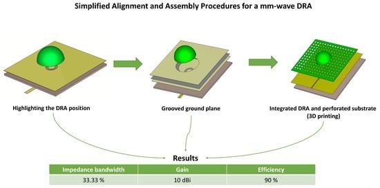
:A wideband hemispherical dielectric resonator antenna (DRA) with enhanced gain is proposed for a frequency band of 20 to 28 GHz. The precise alignment and assembly of the DRA represent key challenges at such frequencies that were addressed using three approaches: the first was based on outlining the DRA position on the ground plane, the second involved creating a groove in the compound ground plane in which the DRA is placed, and the third was based on the 3D-printing of the DRA on a perforated substrate. In all cases, the same DRA was utilized and excited in a higher-order mode using an annular ring slot. The high gain was achieved by exciting a higher-order mode, and the wideband was obtained by merging the bandwidths of the two excited modes. The alignment methods used expedite the DRA prototyping by saving substantial time that is usually spent in adjusting the DRA position with respect to the feeding slot. The proposed configurations were measured, with an impedance bandwidth of 33.33% and a maximum gain of 10 dBi observed. Close agreement was achieved between the measured and simulated results.
1. Introduction
The rapid growth in wireless communications systems, such as mobile communications and the Internet of Things (IoT), has stimulated interest in developing new systems that can operate efficiently in the millimeter wave (mm-wave) frequency band, which provides the required high data rates and capacity [1,2]. However, the main challenge of mm-wave communications is the short propagation range due to attenuation caused by the absorption of oxygen molecules [3]. Therefore, high gain antennas with a stable operation over a wide bandwidth need to be utilized to overcome the signal path loss while transferring massive data, particularly for 5G-and-beyond applications.
Popular antenna types, such as dipole [4], microstrip [5], and monopole [6] have been used in the mm-wave frequency band, albeit with well-known drawbacks, such as narrow bandwidths and increased ohmic losses. On the other hand, a DRA represents a suitable alternative due to the absence of ohmic losses and attractive radiation characteristics that can be achieved through appropriate combination of the resonator dimensions and the relative permittivity, as well as a suitably chosen feeding technique [7]. Therefore, mm-wave single DRAs, as well as arrays, have been reported in several studies over the last few years [8,9,10,11,12,13]. However, DRA alignment and assembly represent key challenges at mm-wave frequencies since any marginal misalignment between the DRA and feeding network can have a significant impact on the antenna’s performance [14,15] due to the shorter wavelengths and the physically smaller antenna size. The same is true for the DRA bonding since the thickness and permittivity of any glue layer can also impact the performance at mm-wave frequencies [16,17]. A further limitation of using a bonding glue layer is the difficulty of achieving uniform thickness, which could alter the mm-wave antenna’s performance. At lower frequencies, DRA-feed alignment is usually achieved by manually adjusting the DRA position for maximum coupling—any misalignment errors are of less significance since the resultant difference in the DRA position is considerably smaller than the operating wavelength. Similarly, the thickness of any bonding material is negligible compared to the wavelength at lower frequencies.
Therefore, DRA prototyping and precise measurements can be cumbersome and time-consuming processes at mm-wave frequencies. As a result, several approaches have been proposed in the literature to address the above limitations. For example, metal fixings and various glue distributions were utilized in [18], which, however, still affect the antenna performance to some extent and involve a relatively complex process. In another study, an acrylic template was proposed in which monolithic polymer-based DRA array elements were placed [19]. However, the acrylic template has a relative permittivity of 2.5, which may impact the mutual coupling between the array elements and excite surface waves that deteriorate radiation efficiency. Furthermore, a 60 GHz circularly polarized substrate-integrated cylindrical DRA array has been reported in which the DRA elements were fabricated and positioned in a single process with no need for additional assembly steps [20]. However, the substrate-integrated DRA approach is most suitable for DRA geometries with uniform cross-sections such as rectangular and cylindrical DRAs. In addition, the height of the DRA is determined by the thickness of the used substrate. An alternative approach proposed is the fabrication of an integrated DRA using low temperature cofired ceramics (LTCC) technology to address DRA alignment and assembly issues [21,22]. However, LTCC technology has a higher prototyping cost and can be associated with surface waves due to the substrate thickness.
In this investigation, simple and low-cost alignment methods are proposed that considerably reduce the required time and effort needed for the assembly and accurate measurement of mm-wave DRAs. Further, the proposed methods can be utilized for DRA geometries of non-uniform cross-section, such as hemispherical, pyramidal and stair-shaped DRAs. Therefore, a wide-band hemispherical DRA was utilized as a case study to demonstrate the potential of the proposed methods for expediting DRA prototyping. The antenna parameters were investigated using the hemispherical DRA mode characteristics equation and CST simulations, as well as measurements. Good agreement was achieved between the simulated and measured results.
The paper is organized into four sections that describe the theoretical and experimental results for three prototypes. The hemispherical DRA configuration and resonance modes are introduced in Section 2. Section 3.1 presents the technique of outlining the DRA position on the ground plane. Section 3.2 describes the method of utilizing a grooved compound ground plane in which the DRA is placed. Section 3.3 focuses on the 3D-printing of the DRA on a perforated substrate. Finally, the conclusions are stated in Section 4.
2. Hemispherical DRA Configuration and Resonance Modes
A hemispherical DRA was selected using alumina with a relative permittivity of = 9.9 and a radius of a = 3.8 mm. The hemispherical DRA supports both transverse electric modes with the as the lowest-order TE mode and transverse magnetic modes with the as the lowest order mode. The subscript n denotes the order of the Bessel function and can be used to determine the elevation variations of the mode’s fields. On the other hand, the subscript m represents the number of full wave field variations along the azimuth axis with . Finally, the subscript s refers to the number of half-wavelength field variations along the r axis. The resonance frequencies of the supported TE modes can be determined from the roots of the following mode characteristics equations [23]:
where and represent the first kind of spherical Bessel function and the second kind of spherical Hankel function of order n, respectively. and represent the derivatives of the aforementioned functions, respectively. is the free space wavenumber and k is the dielectric wavenumber defined as . The roots (a) of Equation (1) were determined numerically from which the resonance frequency of each mode can be calculated as [24]
For the hemispherical DRA under consideration, the resonance frequencies of the first few TE modes were calculated using Equations (1) and (2) and listed in Table 1,
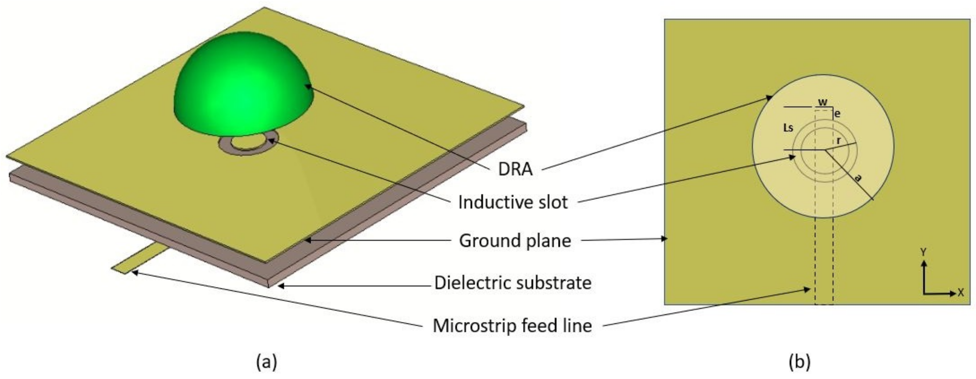
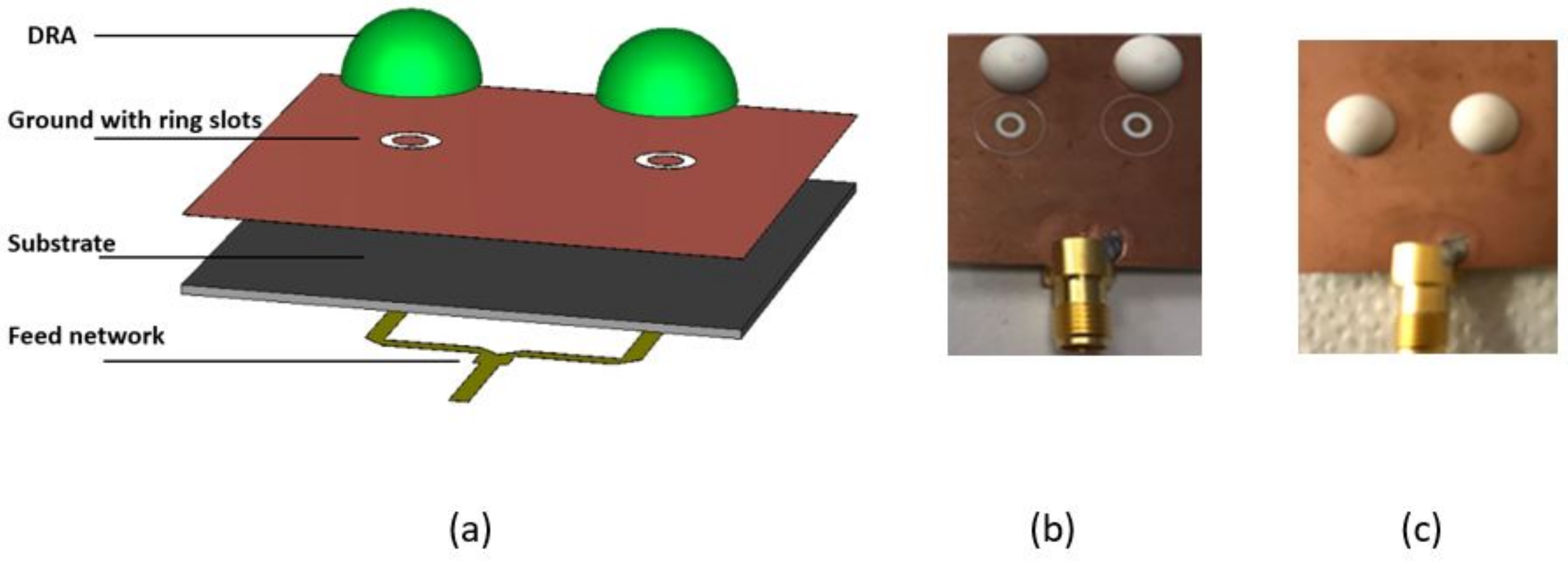
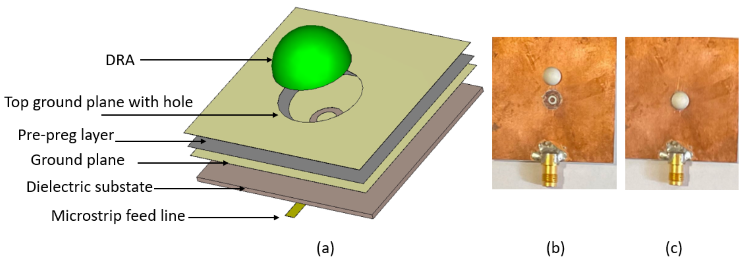
The hemispherical DRA configuration is illustrated in Figure 1a, where it can be observed that the antenna is placed on top of a square ground plane with a size of 20 mm that has an etched annular ring feeding slot. The antenna is fed using a 50 microstrip line with a width of w = 1 mm. The microstrip line is printed on the lower side of a Rogers (RO4350B) dielectric substrate with respective relative permittivity and thickness of 3.48 and 0.5 mm, as demonstrated in Figure 1b.
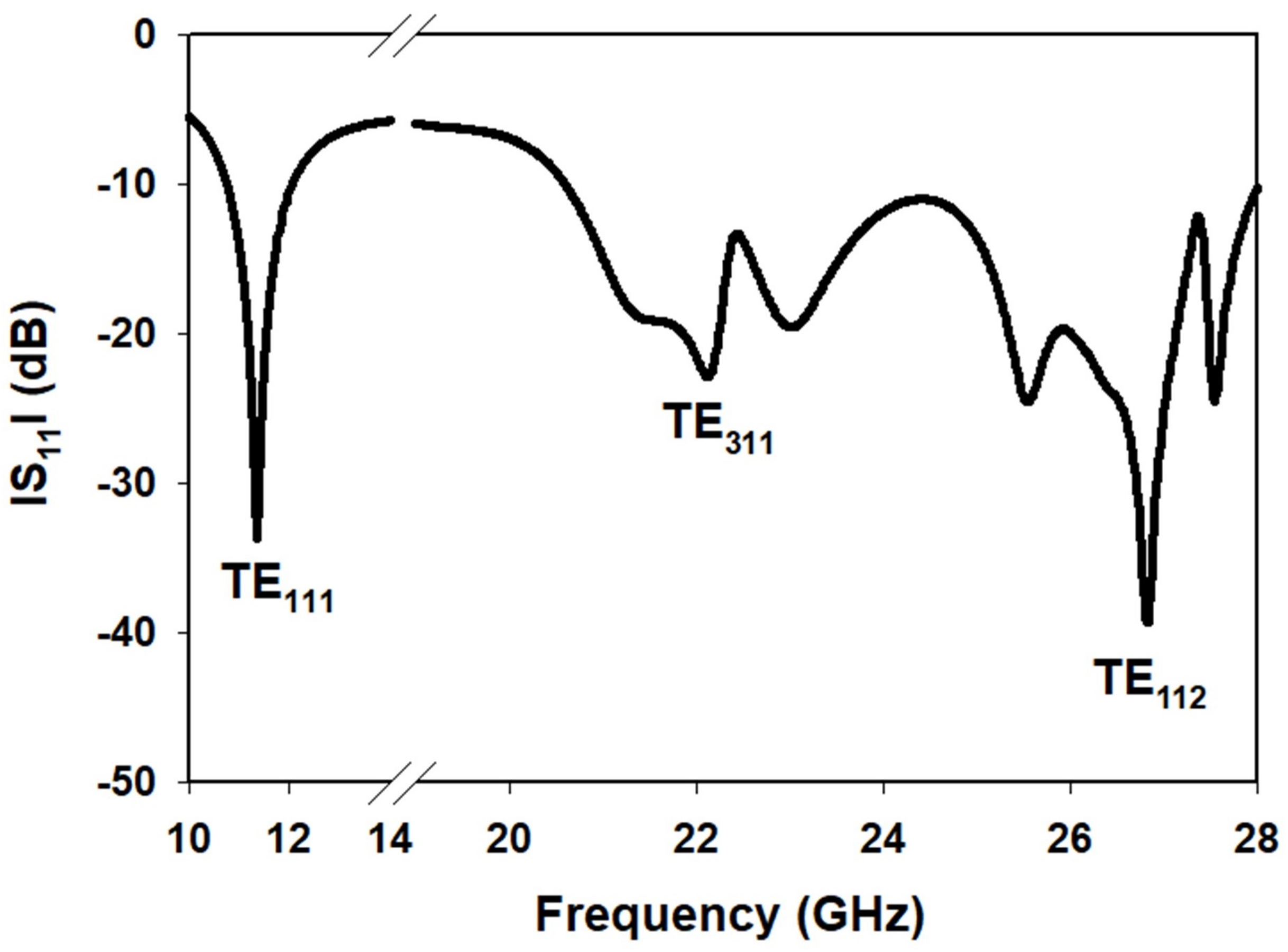
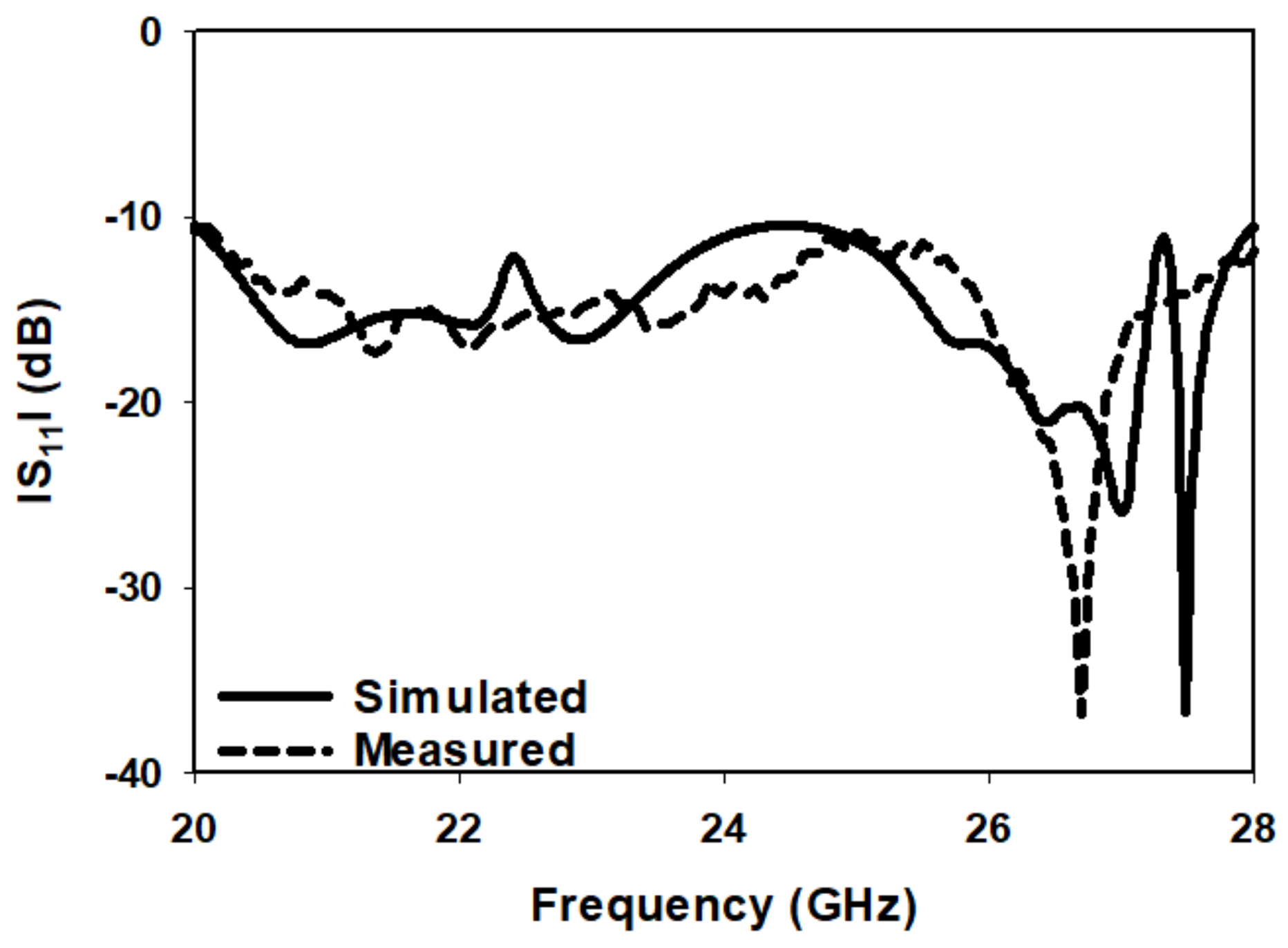
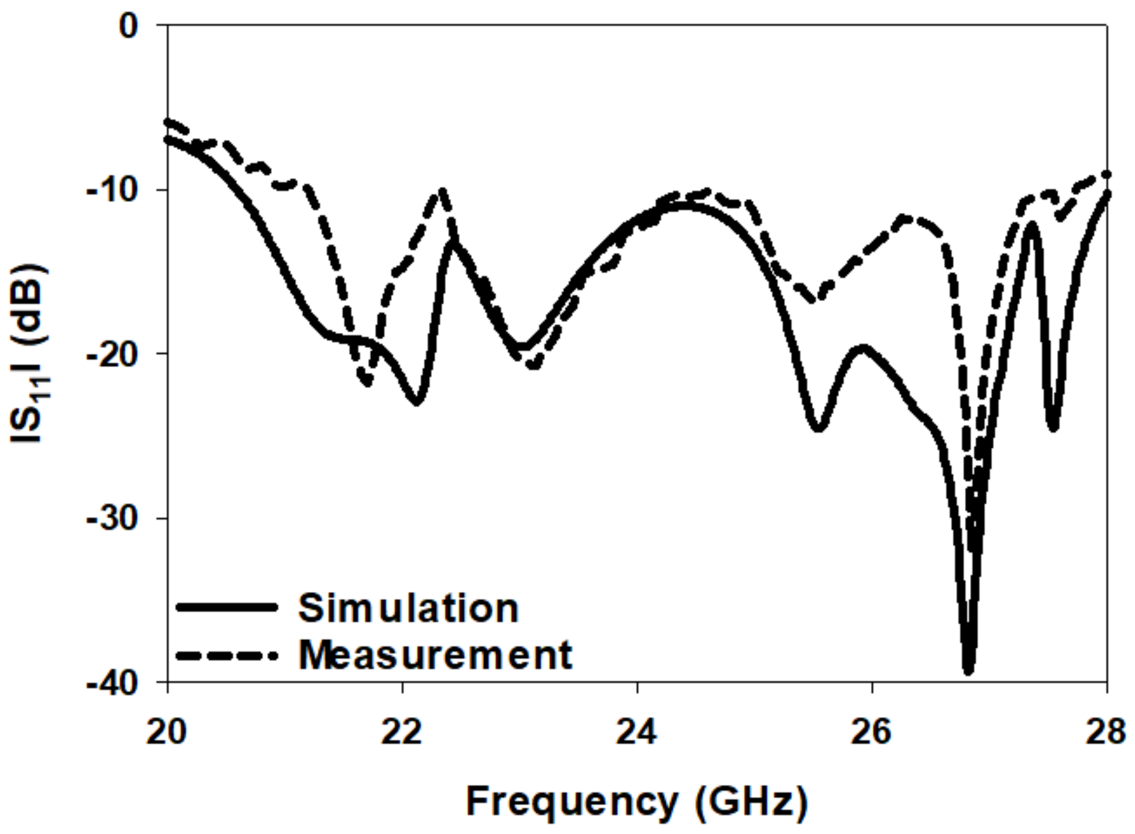
As demonstrated in Table 1, the proposed hemispherical DRA supports two higher-order resonance modes over a frequency range of 20–30 GHz, as well as the fundamental mode at 11.8 GHz. The radius of the annular slot, r, was adjusted for the widest impedance bandwidth that was achieved over a frequency range of 20–28 GHz using r = 1.6 mm with a matching stub length of = 2 mm. The reflection coefficient is presented in Figure 2, where it may be noted that the mode has been excited in conjunction with the higher-order modes of and at 22.5 GHz and 27 GHz, respectively. The simulated resonance frequencies are in close agreement with those calculated using Equation (2). As a result, a wide operating bandwidth of ∼33% was achieved over the expected frequency range. In addition, the antenna offers a stable broadside pattern over the entire frequency range with a maximum gain of ∼10 dBi at 22.7 GHz.
3. Experimental Results
A prototype of the proposed hemispherical DRA was fabricated and measured. The reflection coefficient was measured using a 2.92 mm SMA and an N5245B vector network analyzer (VNA) [25]. In addition, the radiation pattern was measured using the SNF-FIX-1.0 spherical near-field mm-wave measurement system [25]. The proposed simple and low-cost alignment and assembly methods were applied in experimental work as discussed in the following sections.
3.1. Outlining the DRA Position on the Ground Plane
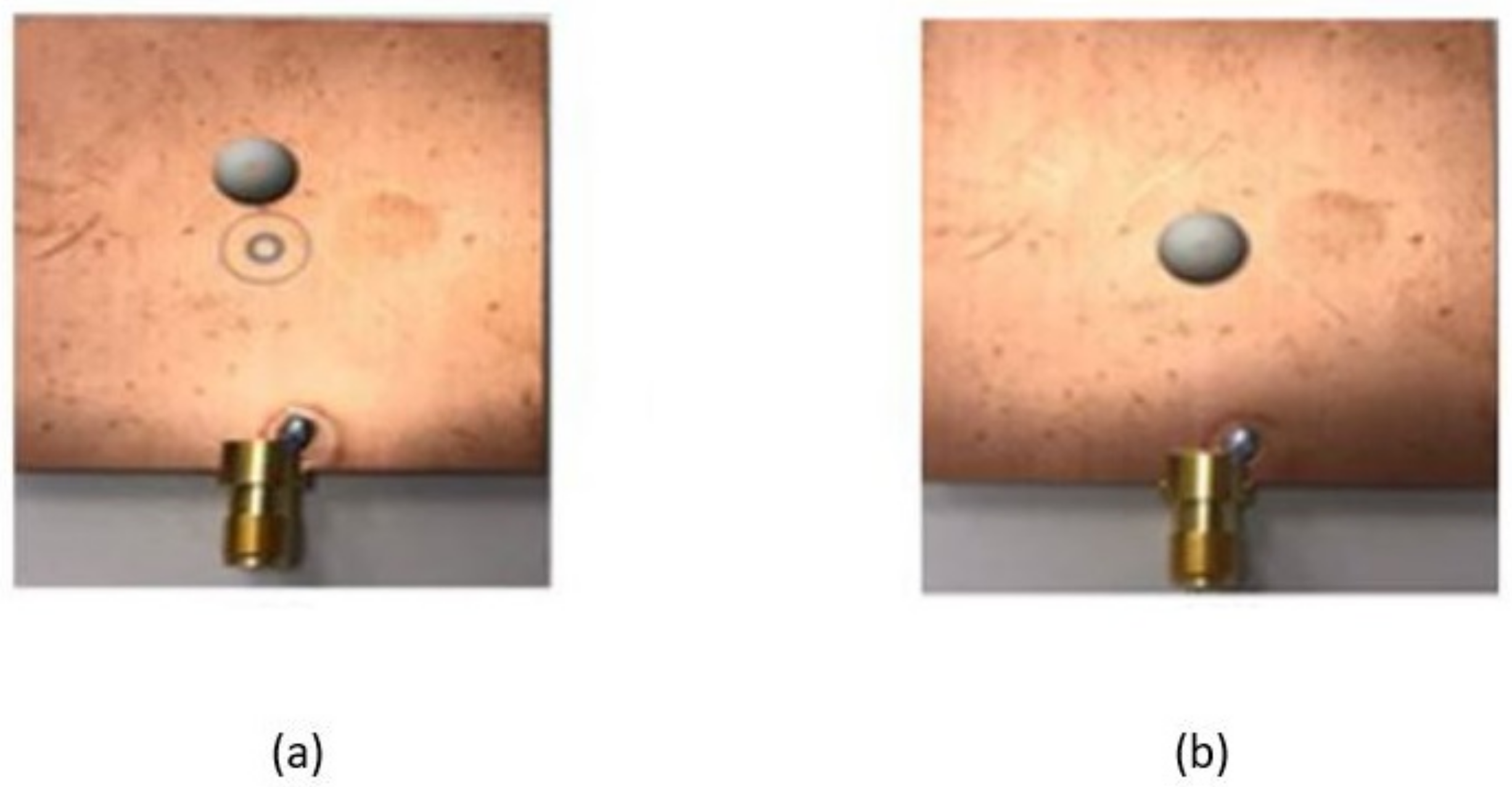
The first alignment method is based on outlining the DRA position on the metal ground plane using white ink, as illustrated in Figure 3. The outlining can be added during the feed network fabrication at no extra cost or added subsequently using a standard 3D-printer. In addition, the automated outlining provides the necessary alignment precision for accurate measurements and saves considerable time that is usually spent adjusting the DRA position. In addition, it eliminates any human errors that may be introduced during attempts to align the mm-wave DRA manually. However, adhesive copper tape is still needed to bond the DRA to the feed network. Therefore, two short pieces of double-sided adhesive copper tape with a thickness of 0.5 mm were utilized to attach the DRA to the ground plane. It should be noted that such a thickness of the copper tape was used in the simulations and was found to have a negligible impact on the antenna performance at frequencies up to 70 GHz.
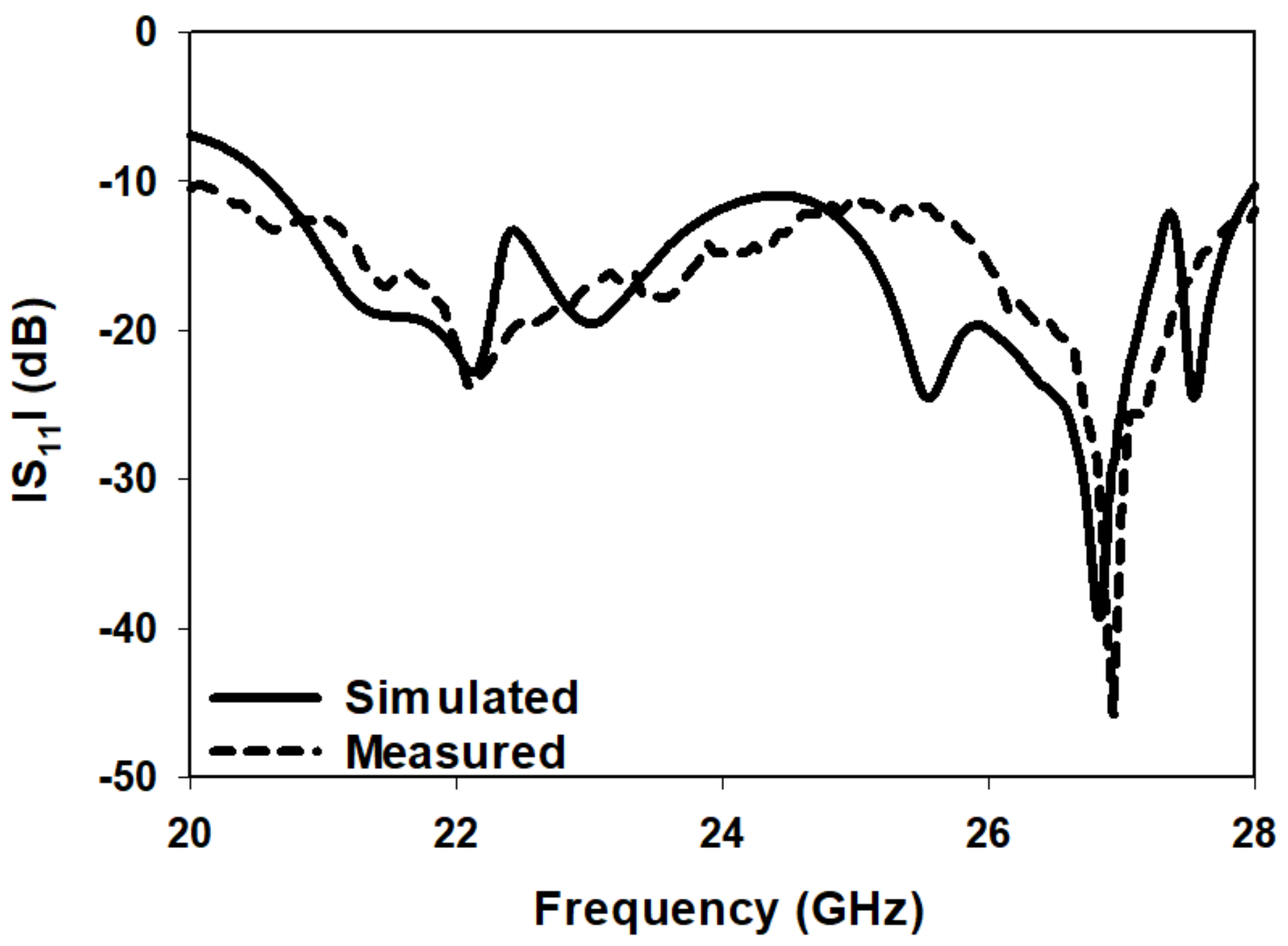
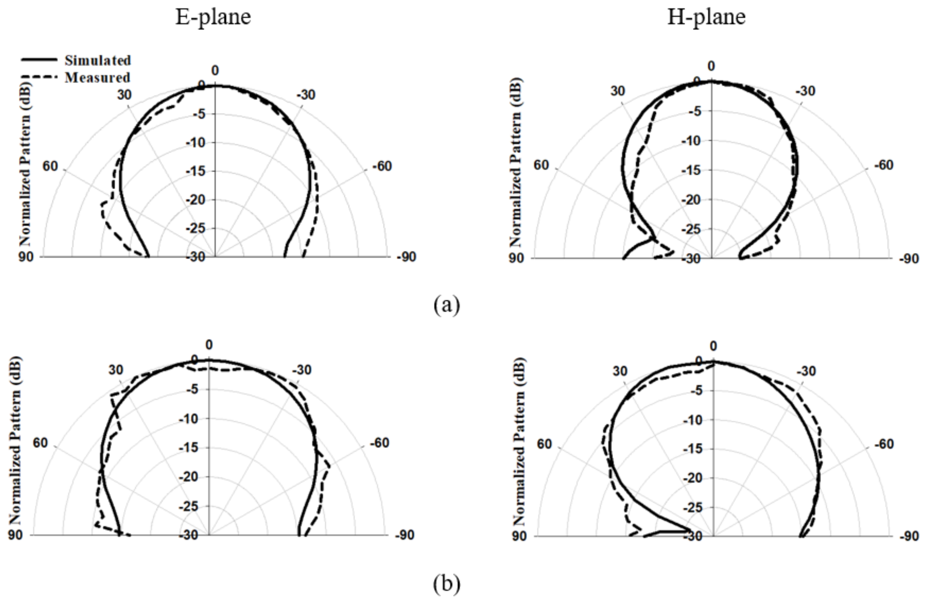
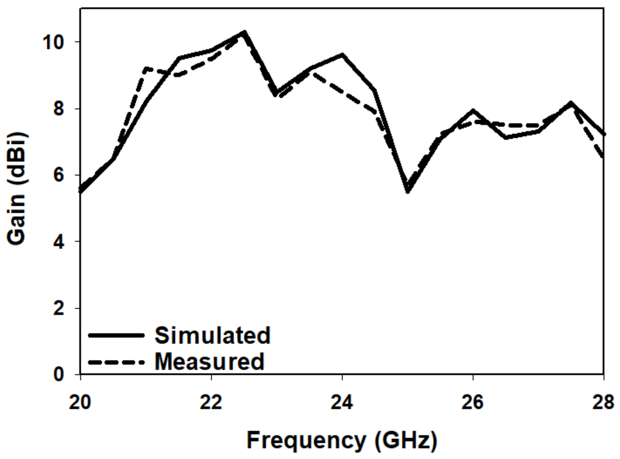
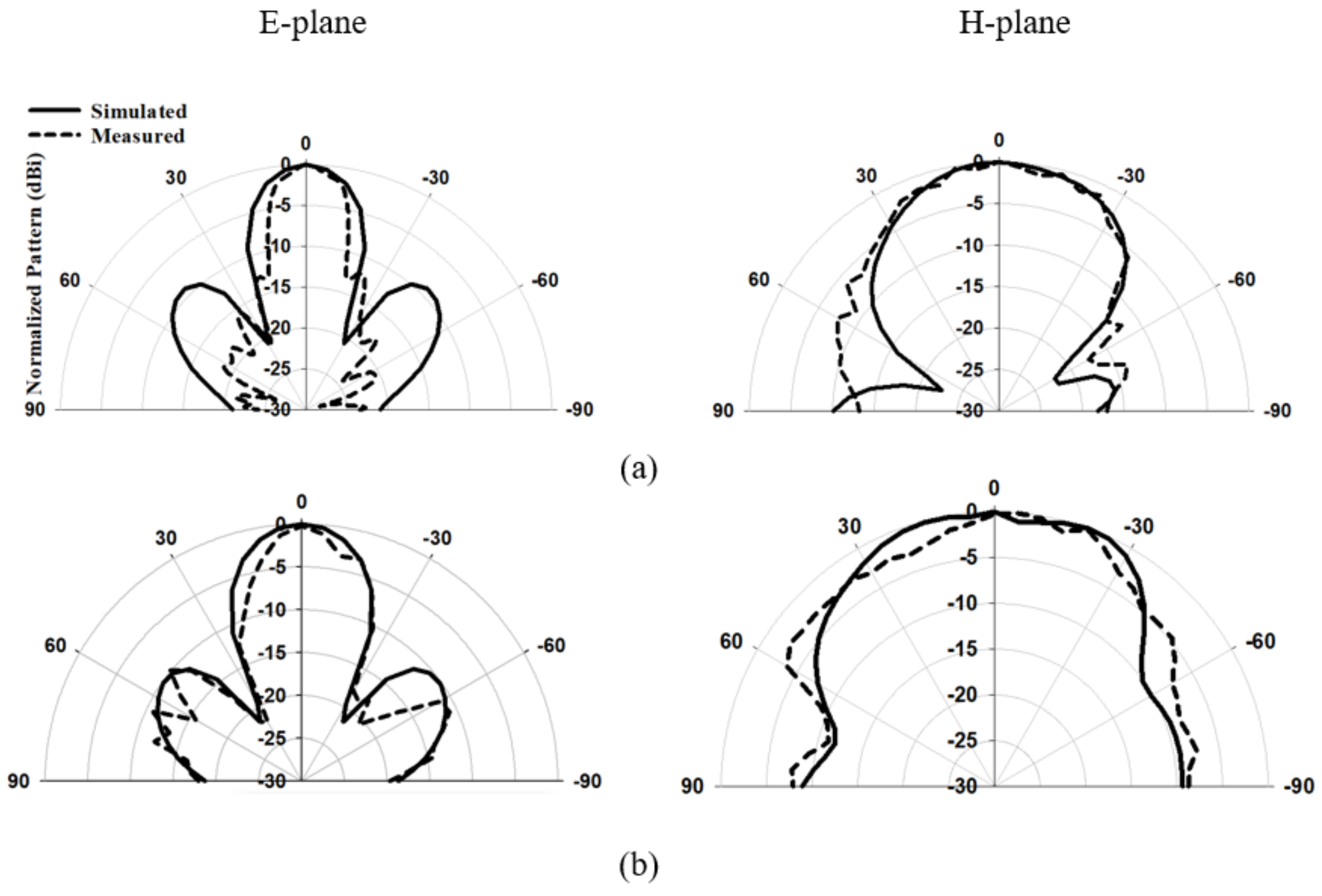
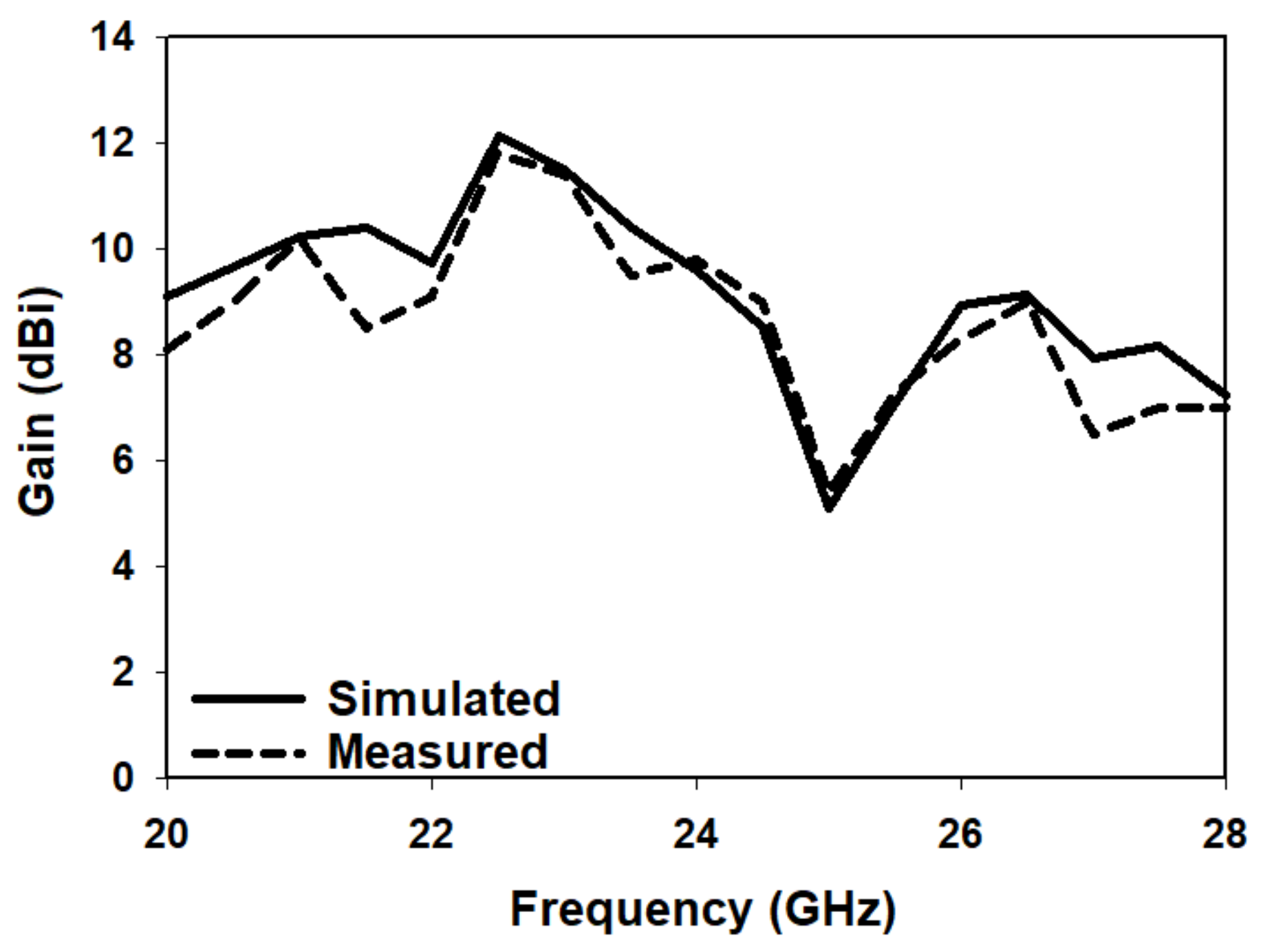
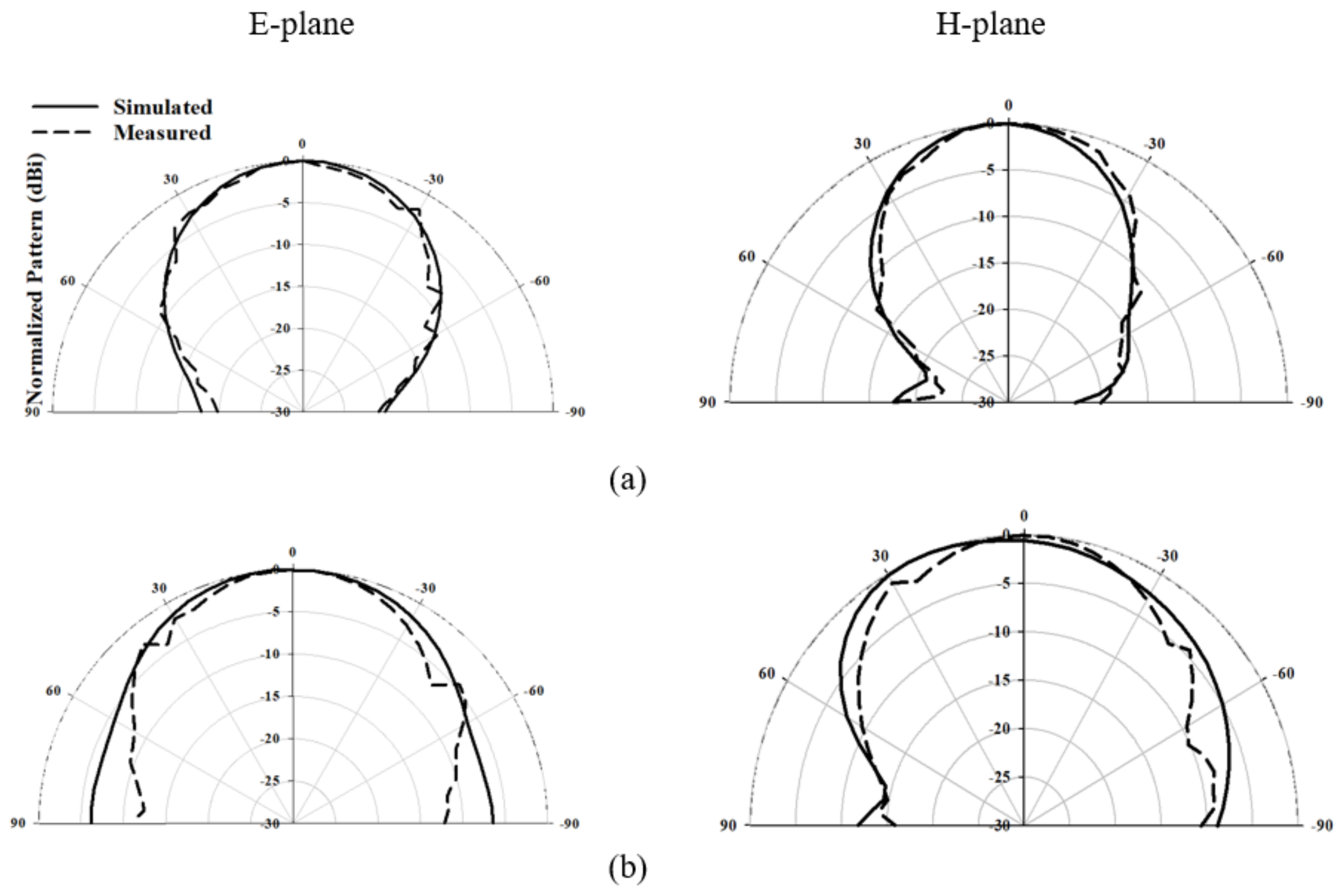
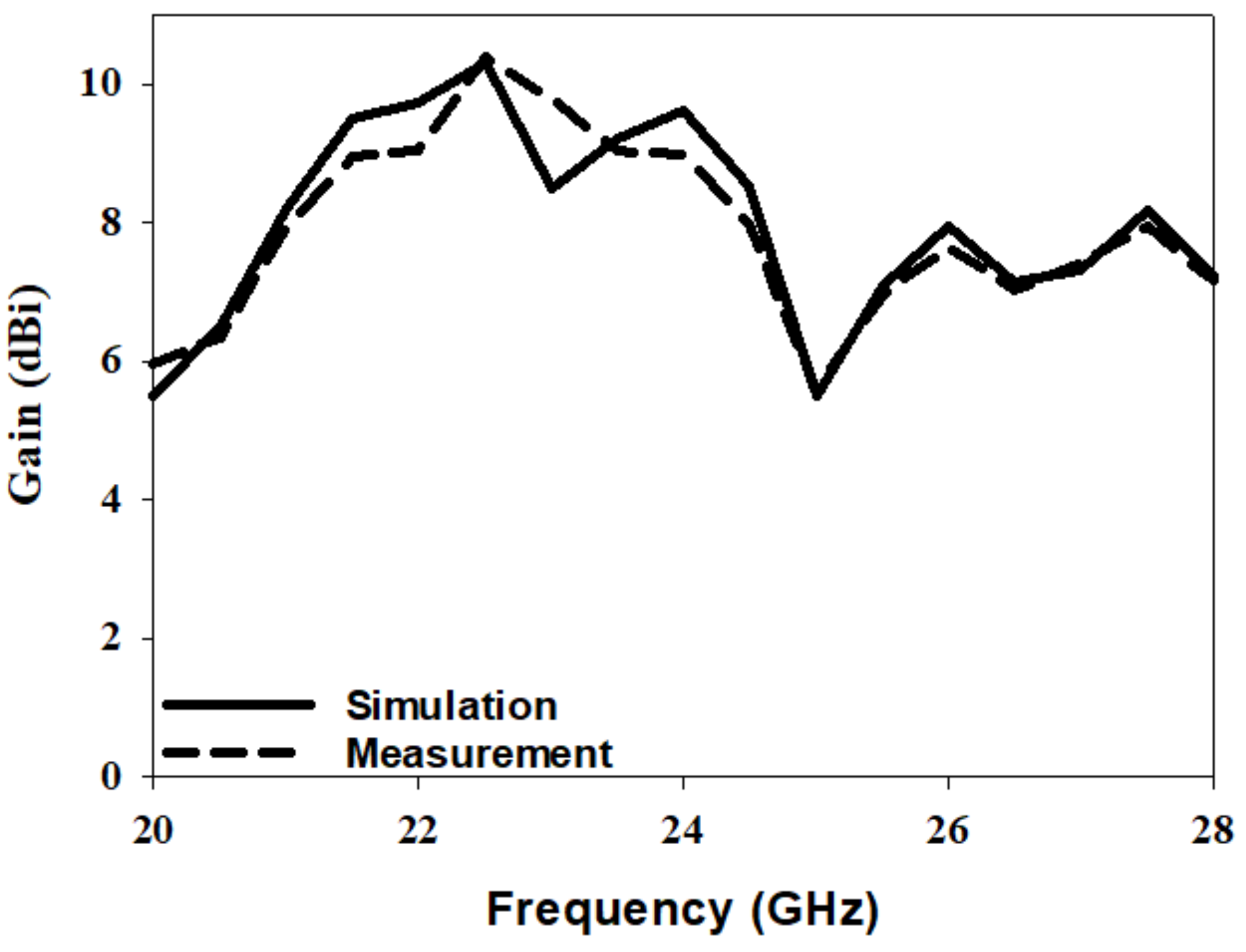
The measured of the proposed DRA is illustrated in Figure 4, where it may be noted that the impedance matching bandwidth extends over the expected frequency range of 20 to 28 GHz, which corresponds to 33.3%, with close agreement between measurements and simulations. The normalized E-plane and H-plane patterns are presented in Figure 5 at 22.7 GHz and 27 GHz. The respective simulated and measured half-ower beamwidths are 61° and 54° at 22.7 GHz, and 70° and 73° at 27 GHz. Again, close agreement was achieved between the simulated and measured results with a stable broadside radiation throughout the operating frequency range. Figure 6 illustrates the simulated and measured realized gain, where it may be noted that the antenna offers an average gain of circa 7 dBi with a peak of circa 10 dBi at 22.7 GHz, which can be attributed to the excitation of a higher-order mode at this frequency. Finally, the simulated and measured gains are in close agreement with each other.
The same approach was utilized for an array of two DRAs that were separated by a distance of 6.6 mm, where the positions of the DRAs are outlined as shown in Figure 7b. Again, a close agreement was achieved between the simulated and measured of the array, as demonstrated in Figure 8, over the desired bandwidth in which the same resonance modes were excited. Figure 9 illustrates the simulated and measured E and H plane radiation patterns of the two hemispherical DRAs operating in and modes, whereby the chosen frequencies were 22.7 GHz and 27 GHz, respectively. The results demonstrate close agreement between the measured and simulated radiation patterns. Figure 10 illustrates the gain of the array configuration, with maximum gains of 12 dBi and 8.5 dBi achieved at 22.7 GHz and 27 GHz, respectively.
From these results, it may be noted that outlining the DRA’s position on the ground plane represents a simple and cost-effective approach that facilitates precise alignment between the DRA and the feeding slot and saves considerable time and effort compared to situations where the DRA position is not outlined. However, the process involves the use of an adhesive copper tape below the DRA, which may be unsuitable at frequencies of more than 70 GHz due to the increased impact of the 0.5 mm gap between the DRA and feeding slot. In addition, the ink used to mark the DRA position may fade with time and usage and, hence, the outlining step may need to be repeated. Therefore, another process for the alignment and assembly of a DRA prototype is proposed in the next section, which offers the same advantages of simplicity, timesaving, and accurate measurement.
3.2. Grooved Compound Ground Plane Alignment and Assembly Process
Introducing a secondary ground plane with a hole was proposed earlier to eliminate the need to use a bonding glue, whereby two separate ground planes were utilized on top of each other with potential air gaps in-between that could have a noticeable impact at higher frequencies [26]. In addition, a small hole needed to be drilled inside the DRA in which a metal holder could be placed to attach the DRA to the ground plane. However, at mm-wave frequencies, it is difficult to drill a hole inside a solid DRA considering the small physical size of the antenna. In this study, a two-ground-planes concept was utilized, where the thickness of each ground plane was chosen to be 18 m. In addition, the required DRA position was determined by etching a circular hole in the top ground plane with a radius larger than that of the DRA by 100 m, as illustrated in Figure 11a. Furthermore, a feeding annular ring slot was etched in the lower ground plane. The two ground planes were bonded together by inserting a thin pre-preg layer in-between with a thickness of only ∼5 m. In addition, a circular hole, identical to that in the top ground plane, was created in the pre-preg layer so that the DRA could be placed directly above the feeding slot without airgaps in-between.
The automated ground plane bonding process was achieved through compression to eliminate potential airgaps between the two ground planes. This compression is part of the feed network fabrication and was implemented by placing the ground planes and pre-preg layer under a vacuum chamber and heating to 180° C under a pressure of 300 psi. Due to the compression, the final thickness of the pre-preg layer was reduced further to ∼2 m. Therefore, the resulting compound structure involves a circular groove with a depth of ∼20 m that precisely accommodates the DRA above the annular ring feeding slot. As mentioned earlier, the diameter of the groove was made larger than that of the DRA by 100 m, i.e., there is a gap of 50 m between the centrally located DRA and the surrounding ground plane from all sides. This gap was filled by adding a double-sided adhesive copper tape along the inner side of the groove, which also served the purpose of bonding the ground plane to the DRA sides. Therefore, no potential airgaps were expected between the DRA and feeding slot. The fabricated grooved compound ground plane and the assembled DRA prototype are presented in Figure 11b,c, respectively.
Figure 12 illustrates the simulated and measured reflection coefficient for a mm-wave DRA that is placed in a grooved compound ground plane. The results demonstrate close agreement between the simulated and measured impedance bandwidths of approximately 33%. Figure 13 demonstrates the simulated and measured E and H plane radiation patterns in and modes with operating frequencies of 22.7 GHz and 27 GHz, respectively. The results demonstrate close agreement between the simulated and measured results. In addition, good agreement was achieved between the simulated and measured realized gains, as illustrated in Figure 14. Furthermore, the grooved compound ground plane offers a simple low-cost process in terms of the DRA assembly and bonding. Therefore, both outlining of the DRA position and using a grooved compound ground plane represent simple and effective processes for rapid prototyping and accurate measurement of mm-wave DRAs. The choice between the two processes depends on the project timeline and budget.
3.3. 3D-Printing the DRA on a Perforated Substrate with the Same Material
The configuration in Figure 15 represents an alternative approach that aims to avoid any misalignment or bonding problems during the DRA assembly. The proposed configuration integrates an alumina hemispherical DRA with a square dielectric substrate of the same material, which facilitates the utilization of 3D-printing technology to fabricate the integrated DRA-substrate structure without needing adhesive material for bonding. For the process, the PCB is fastened against an edge orthogonal to the platen motors. This helps to ensure the sample is not rotated. The printer camera and motors are configured to be accurate to 1/1000 of a millimetre. This is largely an automated process that simplifies the antenna assembly. However, the higher permittivity of the alumina substrate represents a key challenge, and needs to be considerably reduced to minimize the chance of exciting surface waves. A reduced effective relative permittivity can be achieved by creating a perforated alumina substrate with a regular pattern of cylindrical air-filled holes, which means the DRA and substrate can be 3D-printed simultaneously using the same material and 3D-printer.
The resultant perforated substrate’s effective relative permittivity, can be calculated as [27].
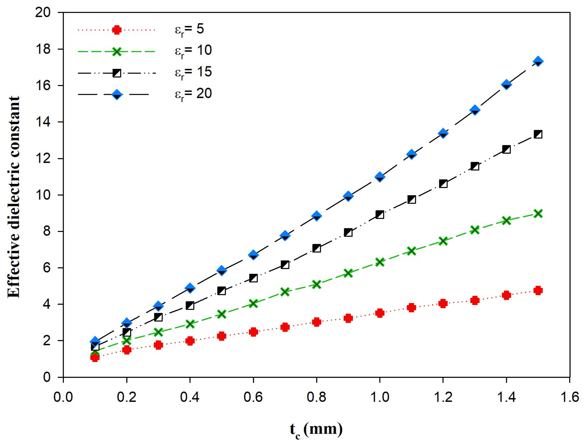
where the spacing between the centres of the two adjacent air-filled holes, 2, can be adjusted for a given so that the required effective relative permittivity is achieved. The unit cell radius and substrate height are fixed as 0.5 and 0.3 mm, respectively.
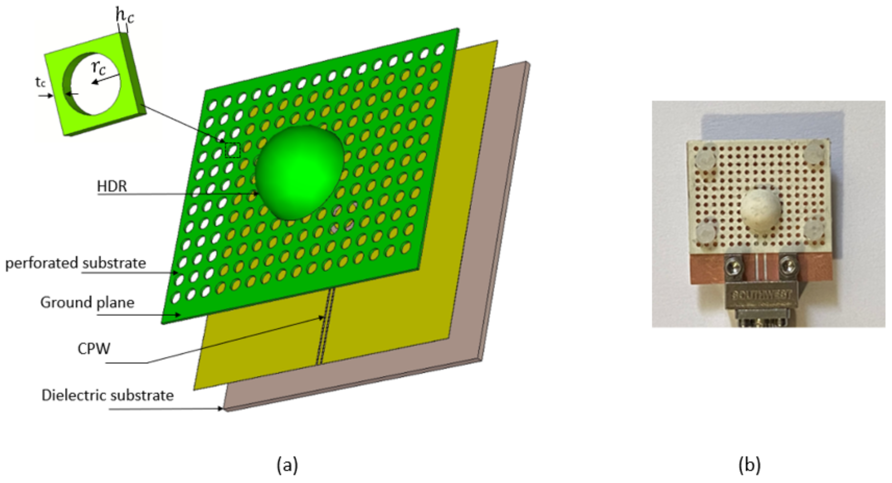
Figure 16 demonstrates the achieved as a function of by changing the substrate relative permittivity from 5 to 20. As can be observed, a linear relationship exists between and . In addition, it is also easy to control the effective permittivity of the perforated substrate by adjusting the diameter of the air-filled holes based on filling ratio theory [28]. Therefore, for an alumina substrate with = 9.9, was chosen as 0.4 mm, so that the effective relative permittivity of the perforated substrate is reduced to = 3, which results in a radiation efficiency of ∼90% across the operating frequency range. Furthermore, the 3D-printed hemispherical DRA was designed using the same DRA radius of previous sections, i.e., a = 3.8 mm. The integrated DRA-substrate structure was fed using a separate feed network that consisted of an annular slot with a radius of 1.5 mm, combined with a coplanar waveguide (CPW) feeding line with a slot width and separation of 0.35 mm and 0.9 mm, as illustrated in Figure 15. The 2.4 mm end-launch connector was affixed to the CPW line that was printed on a Rogers substrate with a relative permittivity of 3.48 and a thickness of 0.5 mm.
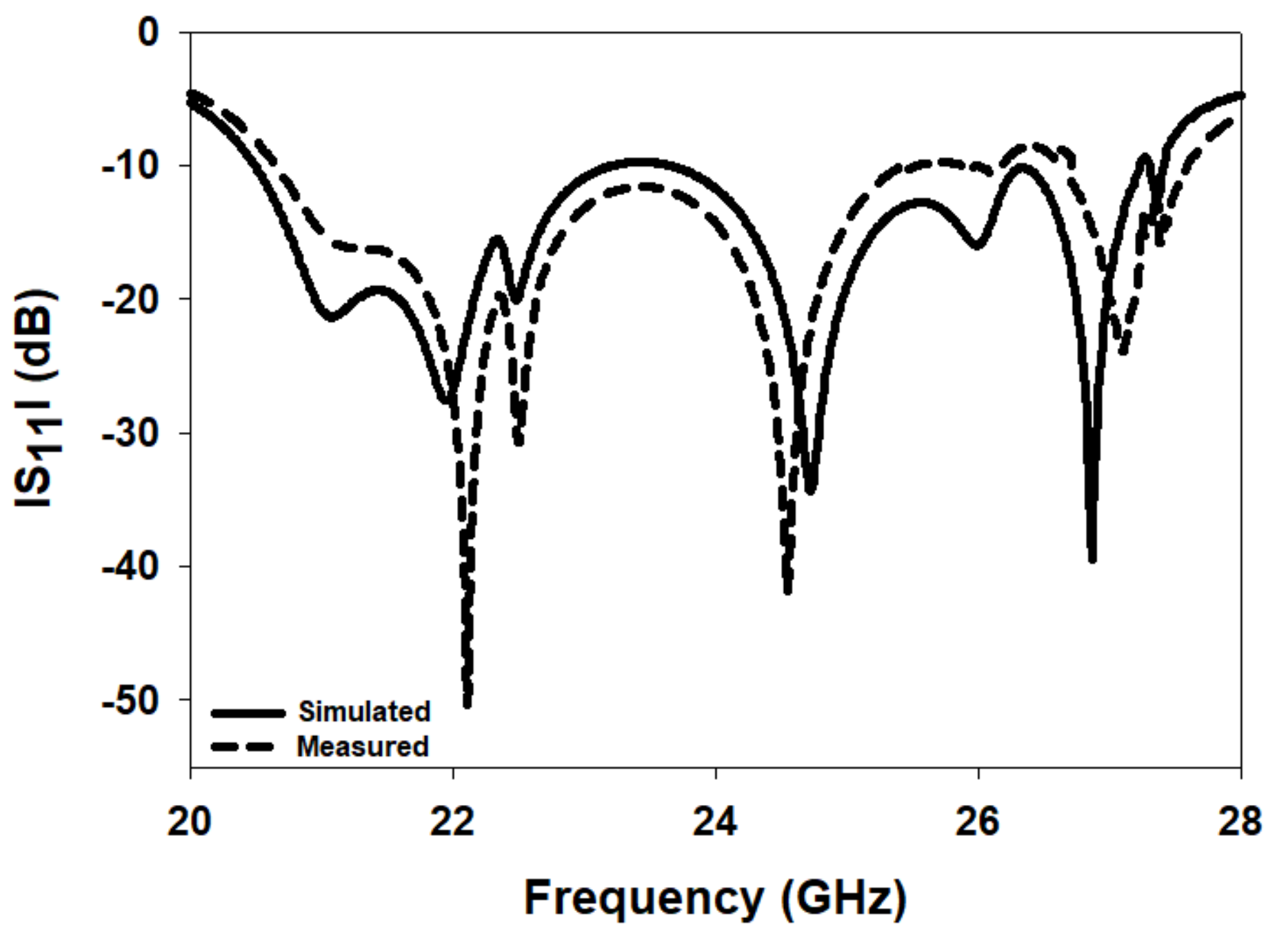
Figure 17 illustrates the measured and simulated reflection coefficients over a frequency range of 20–28 GHz, where the same bandwidth of 33% was achieved in simulations and measurements with a maximum gain of 10 dBi at 22.7 GHz. Figure 18 depicts the E and H plane simulated radiation patterns at 22.7 GHz and 27 GHz for the and modes. The proposed method showed close agreement between the measurements and simulations since an automated process was adopted without using a bonding layer between the DRA and the feeding slot that can impact performance.
Table 2 illustrates a comparison of different approaches that were proposed earlier to simplify the mmwave DRA alignment and/or assembly. This study proposes simple structures in which neither glue nor extra layers are used.
4. Conclusions
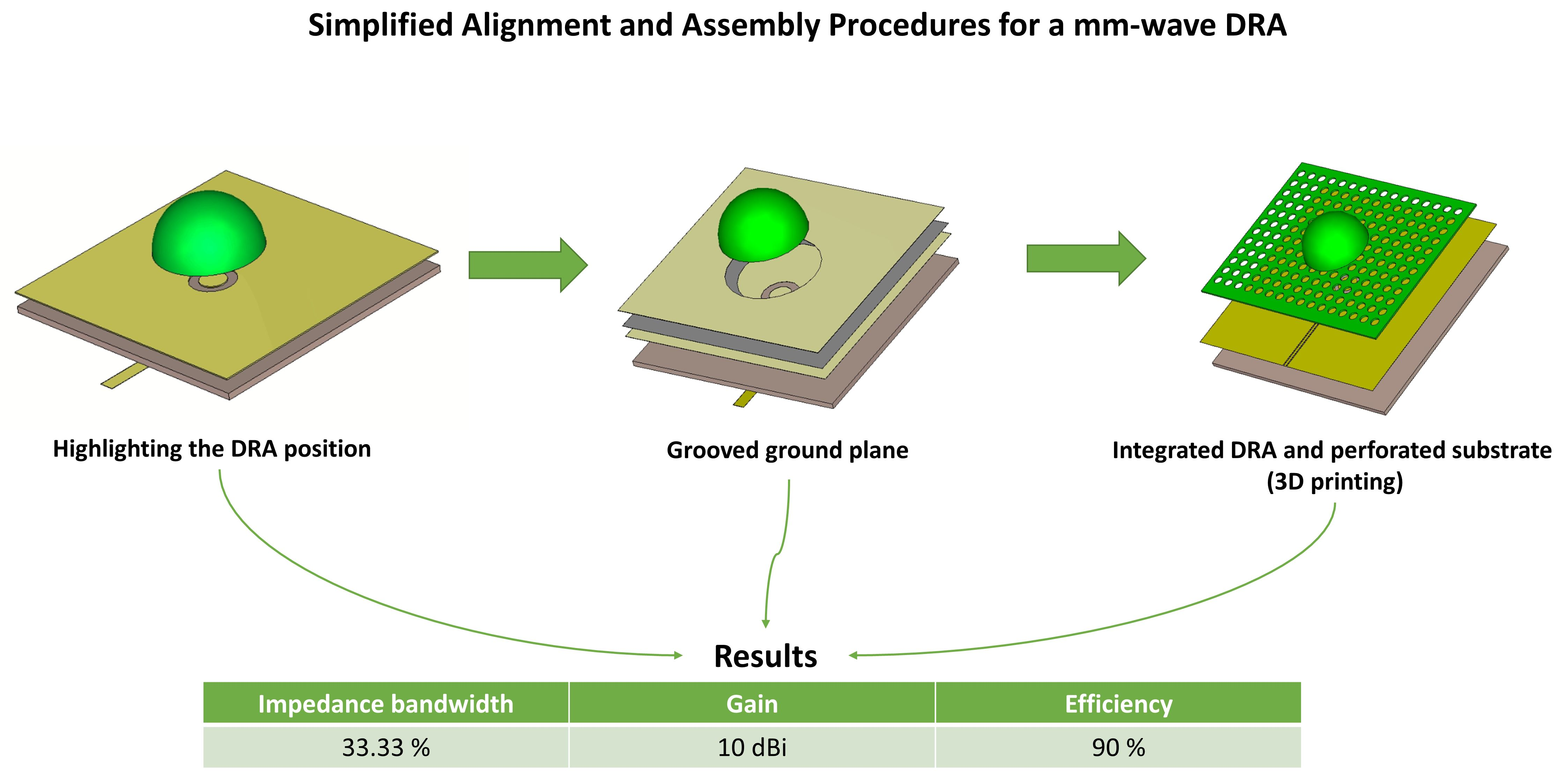
The challenges of alignment and bonding a mm-wave DRA were addressed by proposing three procedures that are based on outlining the position of the DRA on the ground plane, introducing a circular groove in a secondary ground plane to accommodate the DRA and the 3D-printing of an integrated DRA-perforated substrate structure. An array of two DRAs was built and measured using a ground plane over which the DRA positions were outlined. All the prototypes were assessed with close agreement between the simulated and measured results observed. The proposed methods save considerable time that is usually needed for mm-wave DRAs prototyping to achieve a cost-effective approach. In addition, they can be used with any DRA geometries that have uniform or non-uniform cross-sections. The same DRA was used in the three proposed procedures with consistent performance shown in terms of the attractive radiation characteristics, such as an impedance bandwidth of 33% and a maximum gain of 10 dBi. In addition, the proposed methods are largely automated with minimum manual assembly, which improves measurement accuracy. The choice of which method to utilize mainly depends on the project timeframe and fabrication cost. Although all the suggested processes offer low-cost and rapid prototyping of single DRA and arrays with a finite number of elements, the 3D-printing of an integrated DRA-perforated substrate is also suitable for large DRA arrays and large-scale production for 5G-and-beyond communication systems.
Author Contributions
M.D.A.: simulation, manufacturing and measurements, writing; S.K.K.: supervision. All authors have read and agreed to the published version of the manuscript.
Funding
This research received no external funding.
Institutional Review Board Statement
Not applicable.
Informed Consent Statement
Not applicable.
Data Availability Statement
Not applicable.
Acknowledgments
The authors would like to acknowledge the use of the National mmWave Measurement Facility and thank Steve Marsden for his support with the measurements. The authors would also like to thank Bassam Talal from Jouf University for 3D-printing of the integrated DRA.
Conflicts of Interest
The authors declare no conflict of interest.
References
- Lin, W.; Ziolkowski, R.W.; Baum, T.C. 28 GHz compact omnidirectional circularly polarized antenna for device-to-device communications in the future 5G systems. IEEE Trans. Antennas Propag. 2017, 65, 6904–6914. [Google Scholar] [CrossRef]
- Hong, W. Solving the 5G mobile antenna puzzle: Assessing future directions for the 5G mobile antenna paradigm shift. IEEE Microw. Mag. 2017, 18, 86–102. [Google Scholar] [CrossRef]
- Ali, I.; Jamaluddin, M.H.; Gaya, A.; Rahim, H.A. A dielectric resonator antenna with enhanced gain and bandwidth for 5G applications. Sensors 2020, 20, 675. [Google Scholar] [CrossRef]
- El-Halwagy, W.; Mirzavand, R.; Melzer, J.; Hossain, M.; Mousavi, P. A substrate-integrated fan-beam dipole antenna with varied fence shape for mm-wave 5G wireless. In Proceedings of the IEEE International Symposium on Antennas and Propagation and USNC/URSI National Radio Science Meeting, Boston, MA, USA, 8–13 July 2018; Volume 11, pp. 251–252. [Google Scholar]
- Yin, J.; Wu, Q.; Yu, C.; Wang, H.; Hong, W. Broadband symmetrical E-shaped patch antenna with multimode resonance for 5G millimeter-wave applications. IEEE Trans. Antennas Propag. 2019, 67, 4474–4483. [Google Scholar] [CrossRef]
- Wang, J.; Li, Y.; Wang, J. Millimeter-Wave Low-Profile Wideband Magneto-Electric Monopole Antenna. In Proceedings of the 2019 International Applied Computational Electromagnetics Society Symposium-China, Nanjing, China, 8–11 August 2019; Volume 1, pp. 1–2. [Google Scholar]
- Petosa, A.M.M.A.; Ittipiboon, A.; Antar, Y.M.M.; Roscoe, D.; Cuhaci, M. Recent advances in dielectric-resonator antenna technology. IEEE Antennas Propag. Mag. 1998, 40, 35–48. [Google Scholar] [CrossRef]
- Baldazzi, E.; Al-Rawi, A.; Cicchetti, R.; Smolders, A.B.; Testa, O.; van Coevorden Moreno, C.D.J.; Caratelli, D. A high-gain dielectric resonator antenna with plastic-based conical horn for millimeter-wave applications. IEEE Antennas Wirel. Propag. Lett. 2020, 19, 949–953. [Google Scholar] [CrossRef]
- Luo, W.; Shi, L.; Xu, W.; Chen, W.; Yang, Y.; Ren, Y. High Gain Dielectric Resonance Antenna Array for Millimeter Wave Vehicular Wireless Communication. Prog. Electromagn. Res. C 2021, 108, 63–78. [Google Scholar] [CrossRef]
- Kesavan, A.; Al-Hassan, M.A.; Ben Mabrouk, I.; Denidni, T.A. Wideband circular polarized dielectric resonator antenna array for millimeter-wave applications. Sensors 2021, 21, 3614. [Google Scholar] [CrossRef]
- Kremer, H.I.; Leung, K.W.; Wong, W.C.; Lo, K.K.W.; Lee, M.W. Design of dielectric resonator antenna using dielectric paste. Sensors 2021, 12, 4058. [Google Scholar] [CrossRef]
- Chemweno, E.K.; Kumar, P.; Afullo, T.J. Substrate Integrated Waveguide-Dielectric Resonator Antenna for Future Wireless Communication. SAIEE Afr. Res. J. 2022, 3, 119–128. [Google Scholar] [CrossRef]
- Hao, L.; Wang, H.; Li, B.; Yin, W. A New Wideband Circularly Polarized Dielectric Resonator Antenna Loaded with Strips. Int. J. Antennas Propag. 2021. [Google Scholar] [CrossRef]
- Sharawi, M.S.; Podilchak, S.K.; Hussain, M.T.; Antar, Y.M. Dielectric resonator based MIMO antenna system enabling millimetre-wave mobile devices. IET Microwaves Antennas Propag. 2017, 11, 287–293. [Google Scholar] [CrossRef]
- Wahab, W.M.A.; Busuioc, D.; Safavi-Naeini, S. Low cost planar waveguide technology-based dielectric resonator antenna (DRA) for millimeter-wave applications: Analysis, design, and fabrication. IEEE Trans. Antennas Propag. 2010, 58, 2499–2507. [Google Scholar] [CrossRef]
- GLai, Q.; Fumeaux, C.; Hong, W.; Vahldieck, R. 60 GHz aperture-coupled dielectric resonator antennas fed by a half-mode substrate integrated waveguide. IEEE Trans. Antennas Propag. 2010, 58, 1856–1864. [Google Scholar]
- Gong, K.; Hu, X.H. Low-profile substrate integrated dielectric resonator antenna implemented with PCB process. IEEE Antennas Wirel. Propag. Lett. 2014, 13, 1023–1026. [Google Scholar] [CrossRef]
- Boyuan, M.; Pan, J.; Wang, E.; Luo, Y. Fixing and aligning methods for dielectric resonator antennas in K band and beyond. IEEE Access 2019, 7, 12638–12646. [Google Scholar] [CrossRef]
- Qureshi, A.A.; Klymyshyn, D.M.; Tayfeh, M.; Mazhar, W.; Börner, M.; Mohr, J. Template-based dielectric resonator antenna arrays for millimeter-wave applications. IEEE Trans. Antennas Propag. 2017, 65, 4576–4584. [Google Scholar] [CrossRef]
- Sun, Y.X.; Leung, K.W. Circularly polarized substrate-integrated cylindrical dielectric resonator antenna array for 60 GHz applications. IEEE Antennas Wirel. Propag. Lett. 2018, 17, 1401–1405. [Google Scholar] [CrossRef]
- Niayesh, M.; Kouki, A. LTCC-integrated dielectric resonant antenna array for 5G applications. Sensors 2021, 21, 3801. [Google Scholar] [CrossRef]
- Guerrero, R.; Gallée, F.; Kärnfelt, C. Novel 60 GHz DRA topology adapted to the LTCC process. In Proceedings of the 2019 13th European Conference on Antennas and Propagation (EuCAP), Krakow, Poland, 31 March–5 April 2019; pp. 1–5. [Google Scholar]
- McAllister, M.W.; Long, S.A. Resonant hemispherical dielectric antenna. Electron. Lett. 1984, 20, 657–659. [Google Scholar] [CrossRef]
- Sarkar, G.A.; Ballav, S.; Chatterjee, A.; Ranjit, S.; Parui, S.K. Four element MIMO DRA with high isolation for WLAN applications. Prog. Electromagn. Res. Lett. 2019, 84, 99–106. [Google Scholar] [CrossRef] [Green Version]
- UKRI National Millimetre Wave Facility. Available online: https://www.sheffield.ac.uk/mm-wave/ (accessed on 30 July 2022).
- Sarkar, C.; Guha, D.; Kumar, C. Glueless compound ground technique for dielectric resonator antenna and arrays. IEEE Antennas Wirel. Propag. Lett. 2017, 16, 70–74. [Google Scholar] [CrossRef]
- Xia, Z.X.; Leung, K.W.; Lu, K. 3-D-printed wideband multi-ring dielectric resonator antenna. IEEE Antennas Wirel. Propag. Lett. 2019, 18, 2110–2114. [Google Scholar] [CrossRef]
- Liang, M.; Ng, W.R.; Chang, K.; Gbele, K.; Gehm, M.E.; Xin, H. A 3-D Luneburg lens antenna fabricated by polymer jetting rapid prototyping. IEEE Trans. Antennas Propag. 2014, 62, 1799–1807. [Google Scholar] [CrossRef]
- Perron, A.; Denidni, T.A.; Sebak, A.R. High-gain hybrid dielectric resonator antenna for millimeter-wave applications: Design and implementation. IEEE Trans. Antennas Propag. 2009, 10, 2882–2892. [Google Scholar] [CrossRef]
- Chu, H.; Guo, Y.X. A novel approach for millimeter-wave dielectric resonator antenna array designs by using the substrate integrated technology. IEEE Trans. Antennas Propag. 2016, 2, 909–914. [Google Scholar] [CrossRef]
Figure 1.
A slot-fed hemispherical DRA configuration (a) 3D view (b) 2-D top view.

Figure 2.
Simulated of the slot-fed hemispherical DRA.

Figure 3.
The prototype of a hemispherical DRA (a) Highlighted DRA position on the ground plane, (b) Assembled DRA.
Figure 3.
The prototype of a hemispherical DRA (a) Highlighted DRA position on the ground plane, (b) Assembled DRA.

Figure 4.
The of a hemispherical DRA with an outlined position on the ground plane.

Figure 5.
The E and H planes radiation patterns of a hemispherical DRA with an outlined position on the ground plane (a) 22.7 GHz (b) 27 GHz.
Figure 5.
The E and H planes radiation patterns of a hemispherical DRA with an outlined position on the ground plane (a) 22.7 GHz (b) 27 GHz.

Figure 6.
The gain of a hemispherical DRA with an outlined position on the ground plane.

Figure 7.
Configuration of the two hemispherical DRAs (a) 3D layout (b) outlined DRA positions (c) Assembled DRAs.
Figure 7.
Configuration of the two hemispherical DRAs (a) 3D layout (b) outlined DRA positions (c) Assembled DRAs.

Figure 8.
The of an array of two hemispherical DRAs with outlined antenna positions on the ground plane.
Figure 8.
The of an array of two hemispherical DRAs with outlined antenna positions on the ground plane.

Figure 9.
The E and H planes radiation patterns for an array of two hemispherical DRAs with outlined positions on the ground plane (a) 22.7 GHz (b) 27 GHz.
Figure 9.
The E and H planes radiation patterns for an array of two hemispherical DRAs with outlined positions on the ground plane (a) 22.7 GHz (b) 27 GHz.

Figure 10.
The gain for an array of two hemispherical DRAs with outlined positions on the ground plane.
Figure 10.
The gain for an array of two hemispherical DRAs with outlined positions on the ground plane.

Figure 11.
A hemispherical DRA with a grooved compound ground plane; (a) 3D layout, (b) Fabricated DRA with a grooved ground plane, (c) Assembled DRA.
Figure 11.
A hemispherical DRA with a grooved compound ground plane; (a) 3D layout, (b) Fabricated DRA with a grooved ground plane, (c) Assembled DRA.

Figure 12.
The of a hemispherical DRA placed on a grooved ground plane.

Figure 13.
The E and H planes radiation patterns of a hemispherical DRA placed on a grooved compound ground plane (a) 22.7 GHz (b) 27 GHz.
Figure 13.
The E and H planes radiation patterns of a hemispherical DRA placed on a grooved compound ground plane (a) 22.7 GHz (b) 27 GHz.

Figure 14.
Realized gain of a hemispherical DRA placed on a grooved compound ground plane.

Figure 15.
The integrated DRA and perforated substrate configuration (a) 3D layout, (b) Fabricated DRA.
Figure 15.
The integrated DRA and perforated substrate configuration (a) 3D layout, (b) Fabricated DRA.

Figure 16.
The effective permittivity of perforated hemispherical DRA.

Figure 17.
The simulated and measured of the integrated DRA and perforated substrate configuration.

Figure 18.
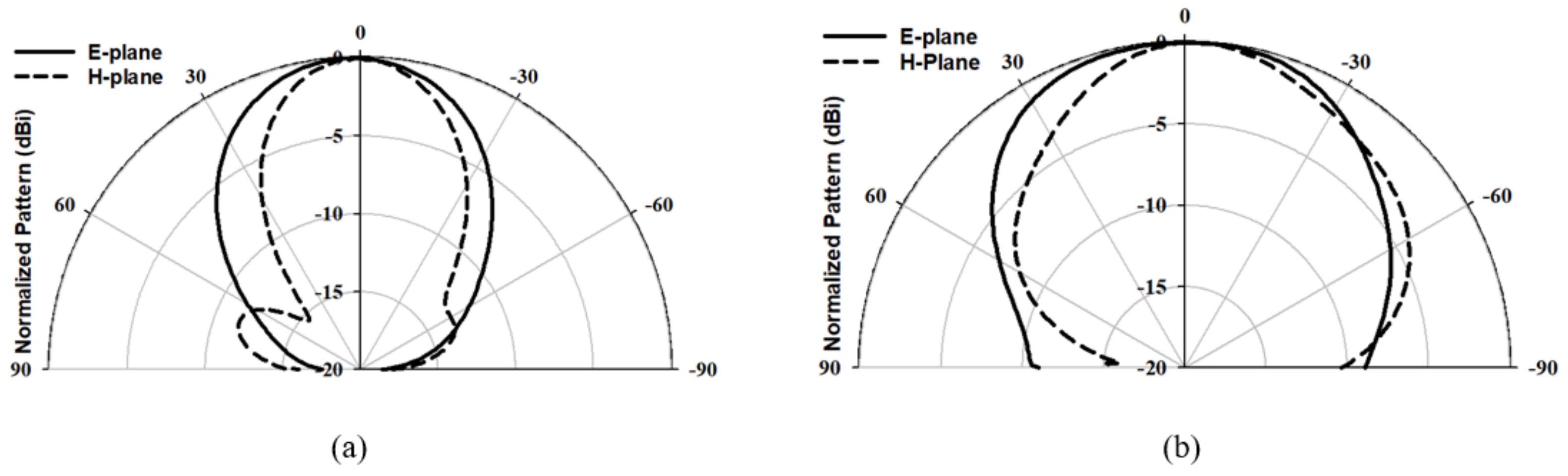
The E and H planes radiation pattern of the integrated DRA and perforated substrate configuration (a) 22.7 GHz (b) 27 GHz.
Figure 18.
The E and H planes radiation pattern of the integrated DRA and perforated substrate configuration (a) 22.7 GHz (b) 27 GHz.


Table 1.
Resonance frequencies of several TE modes of the used alumina hemispherical DRA.
| Resonance TE Mode | Resonance Frequency |
| 17 | |
| 27 |
Table 2.
Comparison between different techniques of DRA fixture and alignment with the proposed designs.
Table 2.
Comparison between different techniques of DRA fixture and alignment with the proposed designs.
| Ref. | Feeding Technique | Comments |
|---|---|---|
| [15] | SIW | Applicable to DRAs with uniform cross-sections only. |
| [16] | Half-mode SIW | Glue was used over the slot for bonding which impacted the performance. |
| [17] | SIW | Glue was used. |
| [19] | Microstrip | Extra layer of acrylic was used, which increased the structure’s size. |
| [20] | SIW | Using fixture holes that affect the performance. |
| [29] | Microstrip | Super glue was used around the DRA and the alignment mark. |
| [30] | SIW | Etching markers and a layer of fixture. |
| This work | Microstrip | CPW and no glue layer is used under the DRA. The grooved compound ground plane overcomes the need for adhesive copper tape below the DRA, as well as any ink fading in case of frequent use of the prototype. The integrated DRA offers automated alignment and bonding. |
Publisher’s Note: MDPI stays neutral with regard to jurisdictional claims in published maps and institutional affiliations. |
© 2022 by the authors. Licensee MDPI, Basel, Switzerland. This article is an open access article distributed under the terms and conditions of the Creative Commons Attribution (CC BY) license (https://creativecommons.org/licenses/by/4.0/).
Share and Cite
MDPI and ACS Style
Alanazi, M.D.; Khamas, S.K. Wideband mm-Wave Hemispherical Dielectric Resonator Antenna with Simple Alignment and Assembly Procedures. Electronics 2022, 11, 2917. https://doi.org/10.3390/electronics11182917
AMA Style
Alanazi MD, Khamas SK. Wideband mm-Wave Hemispherical Dielectric Resonator Antenna with Simple Alignment and Assembly Procedures. Electronics. 2022; 11(18):2917. https://doi.org/10.3390/electronics11182917
Chicago/Turabian StyleAlanazi, Meshari D., and Salam K. Khamas. 2022. "Wideband mm-Wave Hemispherical Dielectric Resonator Antenna with Simple Alignment and Assembly Procedures" Electronics 11, no. 18: 2917. https://doi.org/10.3390/electronics11182917
Note that from the first issue of 2016, this journal uses article numbers instead of page numbers. See further details here.