Article

Investigation of Barrier Layer Effect on Switching Uniformity and Synaptic Plasticity of AlN Based Conductive Bridge Random Access Memory

1
UST-IPPP, College of Electrical and Computer Engineering, National Yang Ming Chiao Tung University, Hsinchu 30010, Taiwan
2
Department of Optoelectronics and Materials Engineering, Chung Hua University, Hsinchu 30012, Taiwan
3
Institute of Electronics Engineering, National Yang Ming Chiao Tung University, Hsinchu 30010, Taiwan
4
Department of Anesthesiology, Cathy General Hospital, Taipei 10630, Taiwan
*
Authors to whom correspondence should be addressed.
Electronics 2022, 11(21), 3432; https://doi.org/10.3390/electronics11213432
Submission received: 29 September 2022 / Revised: 19 October 2022 / Accepted: 20 October 2022 / Published: 23 October 2022
(This article belongs to the Special Issue Quantum and Optoelectronic Devices, Circuits and Systems)

Abstract

:
In this work, we investigated the effect of the tungsten nitride (WNx) diffusion barrier layer on the resistive switching operation of the aluminum nitride (AlN) based conductive bridge random access memory. The WNx barrier layer limits the diffusion of Cu ions in the AlN switching layer, hence controlling the formation of metallic conductive filament in the host layer. The device operated at a very low operating voltage with a Vset of 0.6 V and a Vreset of 0.4 V. The spatial and temporal switching variability were reduced significantly by inserting a barrier layer. The worst-case coefficient of variations (σ/µ) for HRS and LRS are 33% and 18%, respectively, when barrier layer devices are deployed, compared to 167% and 33% when the barrier layer is not present. With a barrier layer, the device exhibits data retention behavior for more than 104 s at 120 °C, whereas without a barrier layer, the device fails after 103 s. The device demonstrated synaptic behavior with long-term potentiation/depression (LTP/LTD) for 30 epochs by stimulating with a train of identical optimized pulses of 1 µs duration.

1. Introduction

The conductive bridge random access memory (CBRAM) has demonstrated enormous potential for energy-efficient non-volatile storage with cognitive computing ability due to its high scalability, large dynamic memory window, good analog conductance switching, and low-off state current compared to valence change memory [1,2,3,4]. The CBRAM is comprised of a simple metal-insulator-metal (MIM) structure with a top electrode made of an electrochemically active metal (e.g., Cu, Ag), a bottom electrode made of an inert metal (Pt, W), and a sandwiched insulating layer that allows the formation and dissolution of nanoscale metallic conductive filaments [5,6,7,8,9]. The cation (Ag+, Cu2+) migration process in filament evolution is functionally equivalent to Ca2+ dynamics of biological synapse and it was previously reported by demonstrating synaptic behaviors including short-term plasticity (STP), long-term plasticity (LTP), and spike-time dependent plasticity (STDP) characteristics [10,11,12,13,14,15]. Despite various attempts to mimic the human brain by utilizing resistive switching architecture, endeavors to match device performance to biological counterparts continue. To justify the suitability for neuromorphic computing, a memristive device must exhibit uniform spatial and temporal switching, long retention, and linear conductance updating capabilities. The defects in the insulating layer and electrode-insulator interface induce uncertainty in the behavior of the conductive filament. Additionally, the inadequate controllability of metal-ion injection and the creation of numerous filaments are implicated in the spatial/temporal switching variability [16,17,18].
As a switching layer in CRAM devices, a variety of chalcogenides (Ag2S, Cu2S), oxides (HfOx, TaOx, and SiOx), and nitride (SiNx and AlNx) based materials have been employed. For these reasons, AlN is a potential contender among these storage media because of its large energy bandgap (6.0 eV), high thermal conductivity (285 W/m.K), and greater thermal stability, all of which result in enhanced switching behavior. It is also much more compatible with nitride electrodes (TiN and TaN), which are common in semiconductor production foundries. Moreover, AlN-based memory could be easily integrated with power electronics devices, including nitride compound semiconductor-based high electron mobility transistors (HEMTs) [19] that can drive high-speed memristors. The anion migration-based AlN RRAM has shown energy-efficient ultra-high switching speeds and high-density multilevel storage capabilities [20,21]. Recently, the high-performance cation migration-based resistive switching operation of the AlN CBRAM device has been reported for non-volatile storage applications. The switching instability remains the main problem in CBRAM devices due to uncontrolled drift and diffusion of metal-ion species from the active electrode to the switching layer during switching cycles.
Several techniques such as the insertion of a metal layer [22], employing a composite electrode [23], embedding a metal nano-island array [24], and the alloying of conduction channels [25] were deployed to improve the switching stability of the CBRAM device. Compared to other techniques, the insertion of the barrier layer is a cost-effective and easy-to-fabricate method. Transition metals such as titanium, tantalum, and tungsten have been extensively studied as diffusion barrier materials due to their immiscible characteristics with copper [26,27,28]. Metal nitrides act as better barrier layers compared to their metal parts as nitridation improves chemical stability [29]. The diffusion barrier properties of WNx in copper interconnect and microelectronic circuits have already been reported [30,31]. WNx has shown better barrier properties for the copper electrode as nitrogen does not react with copper and smaller-size nitrogen molecules fill the void, reducing the diffusion of copper [32]. In this work, we propose the insertion of the WNx barrier layer to enhance the switching uniformity by limiting Cu diffusion into the switching layer. The reliability characteristics, such as endurance and data retention characteristics, improved significantly with barrier layer insertion. To further demonstrate the suitability of the CBRAM device for neuromorphic applications, the long-term potentiation and depression synaptic activity are illustrated with superior linearity.

2. Materials and Methods

The schematic device processing started with the deposition of 500 nm thermally grown SiO2 on a RCA cleaned Si wafer as an isolation layer. For the bottom electrode, a 20 nm Ti adhesion layer with a Pt layer of 60 nm thickness was deposited by a DC sputtering system. Then an AlN switching layer of 10 nm thickness was deposited at room temperature in a mixed Ar and N2 ambient atmosphere using DC sputtering at a working pressure of 7.6 mTorr. Prior to patterning the top electrode, a 7 and 10 nm thick WNx diffusion barrier layer was deposited by DC sputtering at room temperature by maintaining the flow rate of Ar and N2 at 24 sccm and 12 sccm, respectively. Subsequently, an 80 nm thick Cu layer was deposited as the top electrode using DC sputtering at room temperature to complete the stacked device structure. Both the barrier and the Cu top electrode were patterned using a circular metal shadow mask to a diameter of 120 µm. The electrical DC and pulse characteristics were performed with the Agilent B1500/B1530 semiconductor parameter analyzer. The Cu top electrode was always biased with DC and pulse signals, while the Pt bottom electrode was grounded in the electrical measurement setup. The structural information of the device was taken by using a JOEL JEM-2010 transmission electron microscope (TEM).

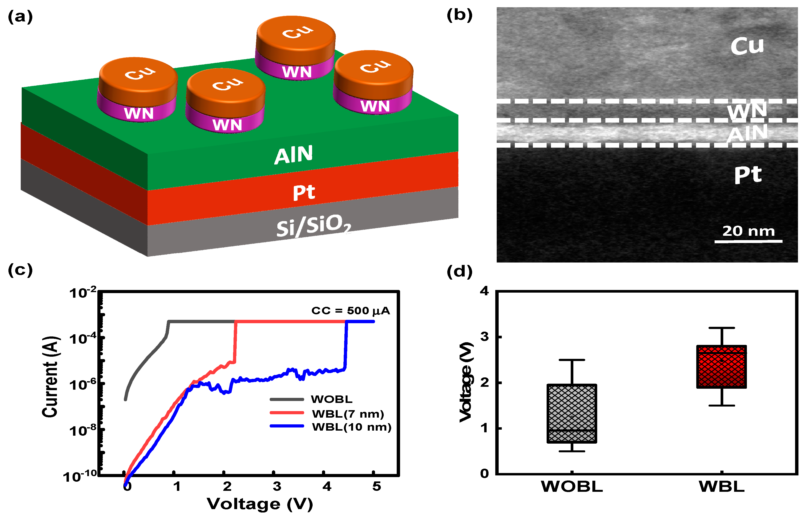
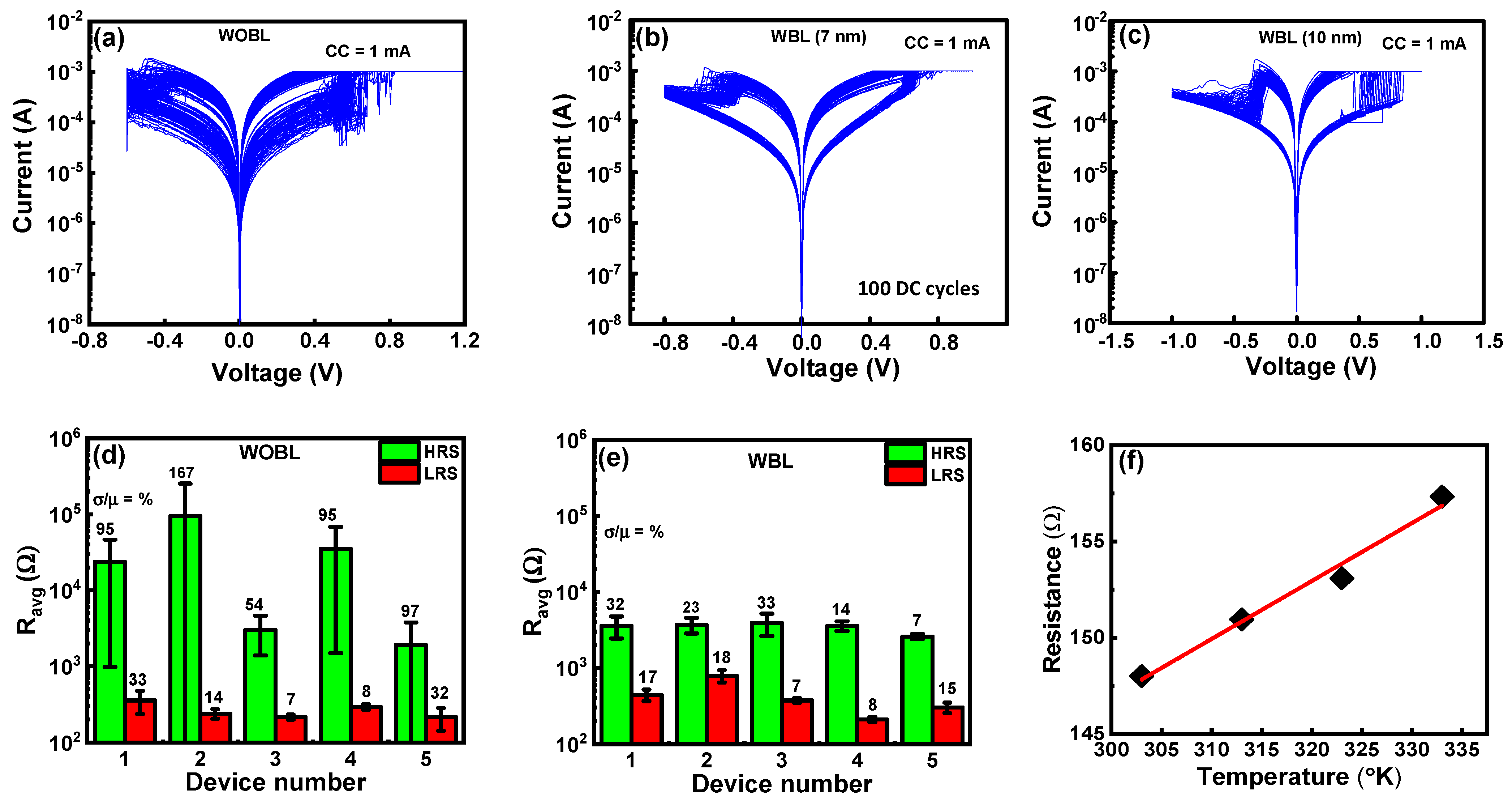
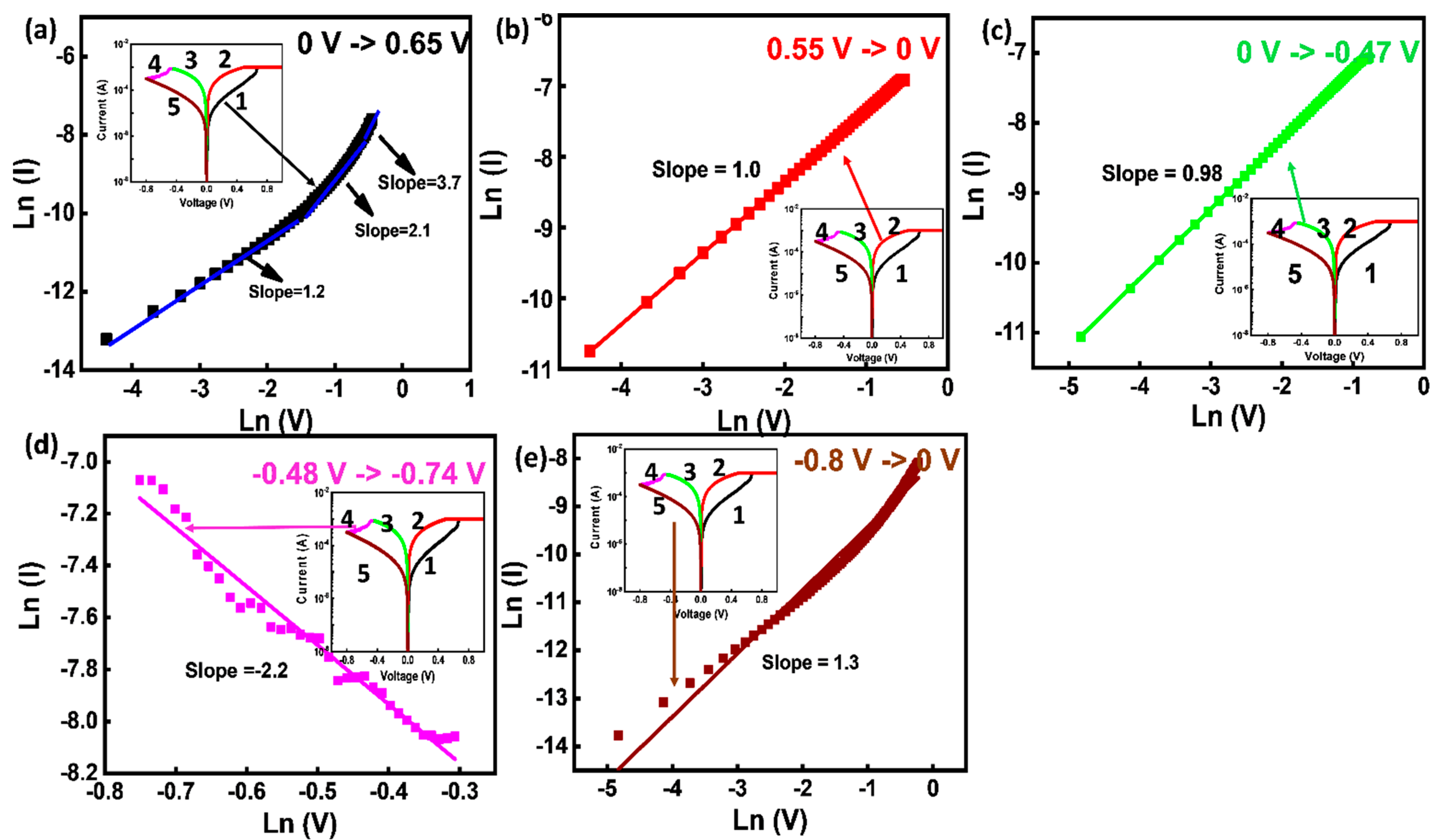
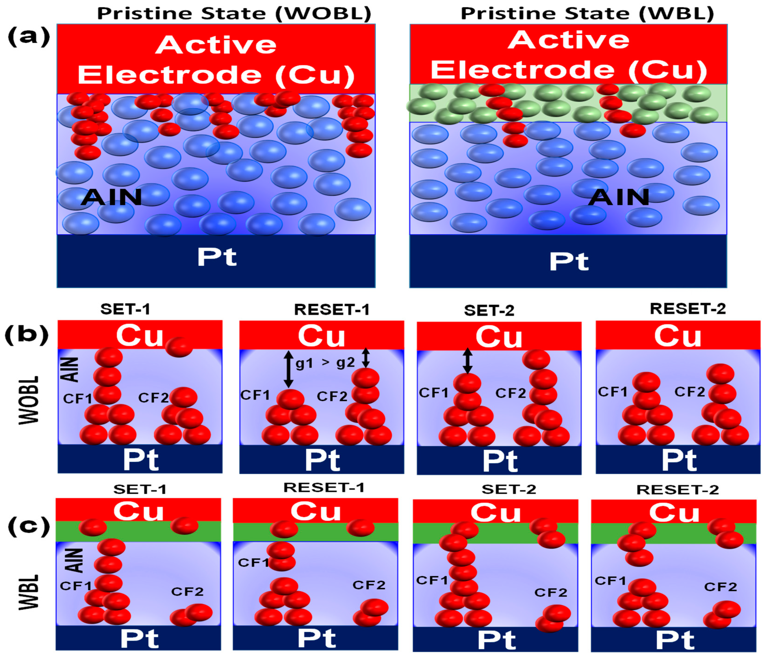
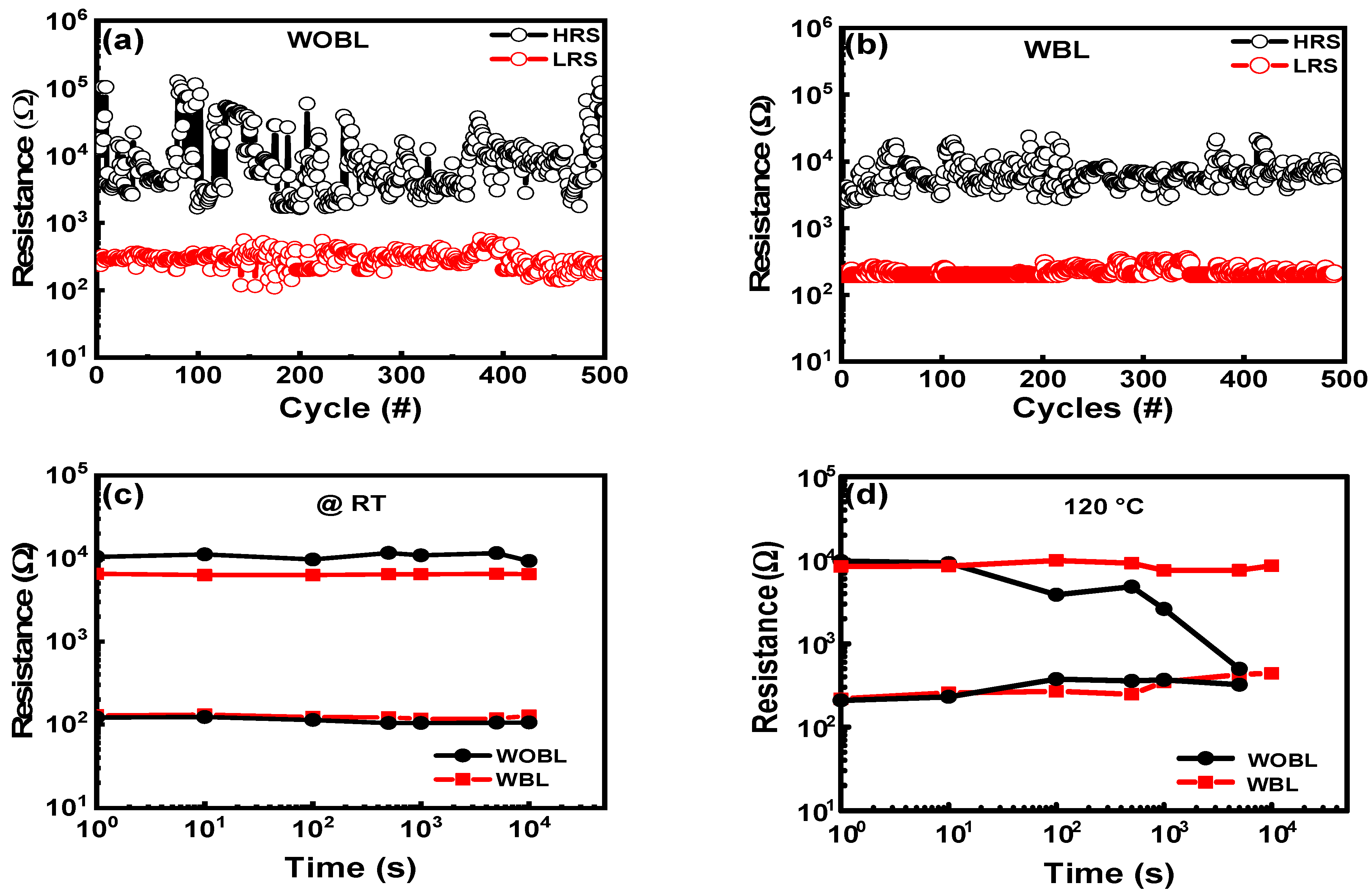
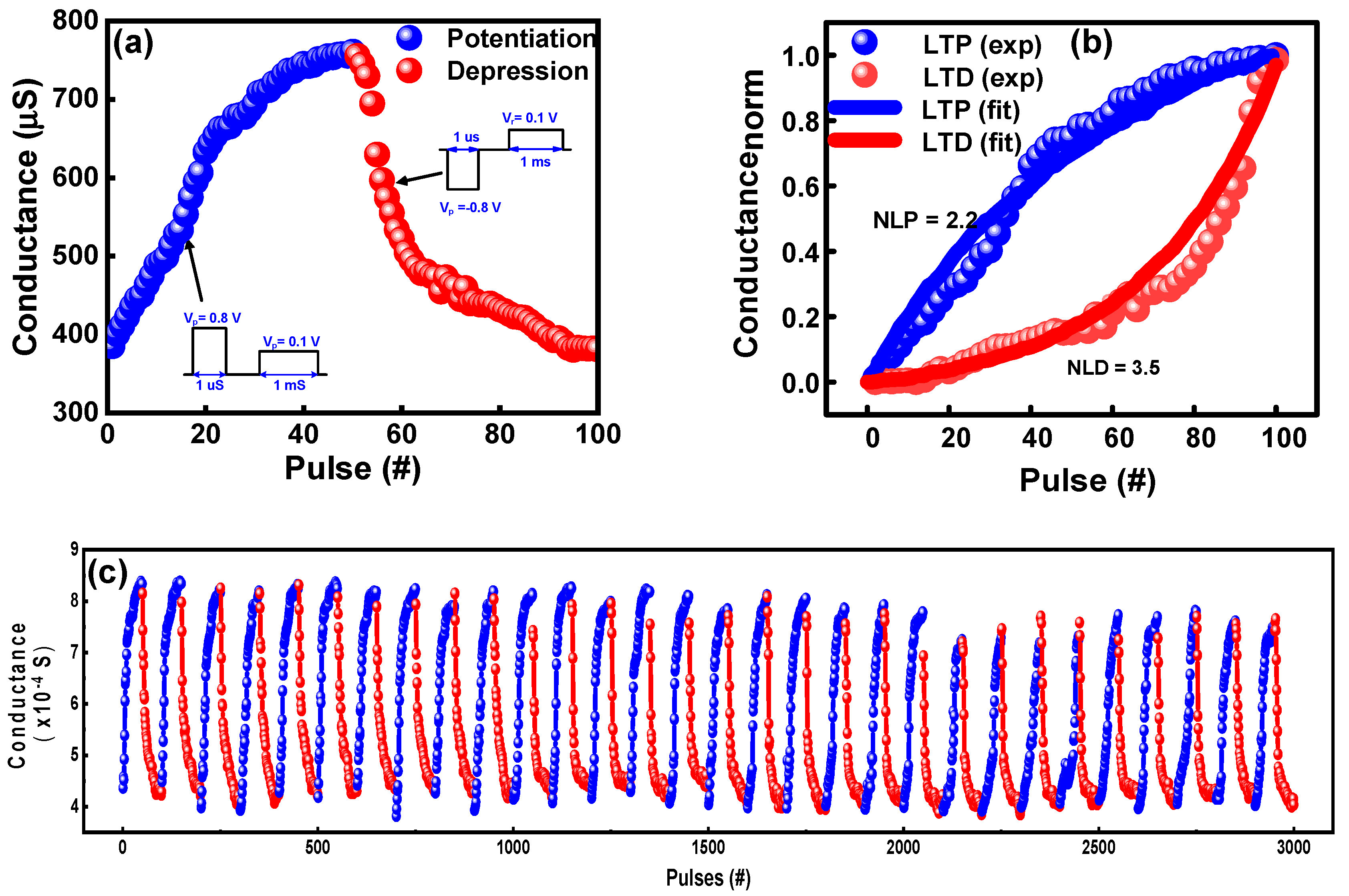
3. Results and Discussion

Figure 1a depicts the schematic layout of the proposed Cu/WNx/AlN/Pt CBRAM device. The cross-sectional TEM image of the device shown in Figure 1b clearly indicates the multiple layers in the stacked structure. The device switches from a high-resistance pristine state to a low-resistance state called the forming process. The forming behavior of without barrier layer (WOBL) and with barrier layer (WBL) devices shown in Figure 1c confirms a larger leakage current with low forming voltage in WOBL devices due to the diffusion of copper into the switching layer during top electrode deposition [33,34]. The insertion of the WNx barrier layer, which prevents copper diffusion, reduces the leakage current and increases the forming voltage. The result shows with a thicker WNx barrier layer (10 nm), forming voltage increases undesirably and during resistive switching operation, it shows volatile operation. Hence, a WBL device with a barrier layer thickness of 7 nm was compared with the WOBL device for further investigation. The forming voltage distribution for 10 devices is shown in Figure 1d. The average forming voltage of the WOBL device is 1.2 V, whereas it is 2.5 V for the WBL device. The device-to-device variation of Vforming is larger in the case of the WOBL device and is mainly due to uneven spatial copper diffusion into the AlN switching layer.
Figure 2a,b show the typical DC current-voltage characteristics of the WOBL and WBL devices. Both devices exhibit bipolar switching behavior with a positive bias sweep of 1.2 V at a compliance current (CC) of 1 mA for set operation and a negative sweep of −0.8 V for reset operation, respectively. From the measured 100 DC switching cycles, we observed that the WOBL device shows larger cycle-to-cycle variation in HRS/LRS compared to the WBL device. Without the barrier layer, multiple incomplete conductive paths are formed by the diffusion of copper into the AlN layer during the forming process, which subsequently causes variation in set/reset switching cycles. The device-to-device and cycle-to-cycle on/off resistance distribution is plotted in Figure 2c,d with each device tested for 30 DC cycles. The on-state resistance, LRS, of WOBL devices is significantly lower compared to WBL devices. This indicates filament formation through a large amount of Cu ion migration. The WOBL devices show the worst-case coefficient of variances (σ/µ) of 167% and 33% for HRS and LRS, respectively. In the case of the WBL, the variations improved significantly to 38% and 18%, respectively. This result confirms the switching stability with the insertion of the barrier layer. The resistance at LRS increases with the increase of temperature, which confirms the metallic nature of the conductive filament shown in Figure 2f. From the resistance-temperature plot, the temperature resistance coefficient is calculated by using Equation (1) [35]:
R ( T ) = R 0 [ 1 + α ( T T 0 ) ]
where R0 is the resistance at temperature T0 and α is the temperature coefficient of resistance. The estimated α = 0.003 confirms the formation of a Cu filament during the on state.
The conduction mechanism of the Cu/WNx/AlN/Pt CBRAM cell was investigated by analyzing the ln(I)~ln(V) graph in different regions as shown in Figure 3. The I-V curve between 0 and 0.25 V with a slope of 1.2 is well-fitted with the ionic conduction Equation (2) given by [36,37]:
ln ( j )   α   ln ( V ) ( ln T + a / T )
where J, V, a, and T are current density, bias voltage, constant, and temperature. This equation explains that ionic conduction occurs due to the oxidation of electrochemically active metal Cu into Cu ions and then the migration of Cu ions to the Pt bottom electrode with the application of positive bias to the top Cu electrode. The Cu ions are reduced at the bottom Pt electrode and the metallic conductive filaments grow from the bottom electrode to the top electrode, making the connection between the electrodes. As the applied bias voltage increases, the diameter of the filament becomes thicker, resulting in higher slopes of 2.1 and 3.7 between 0.25 to 0.58 V and 0.58 to 0.65 V, respectively. Due to the presence of the WNx barrier layer, there is a gradual increment in slope. During biasing from 0.55 to 0 V, the current plot fitted well with the ohmic conduction mechanism which can be expressed by Equation (3):
ln ( j )   α   ln ( V )     a / T
where J, V, a, and T are current density, bias voltage, constant, and temperature. The current conduction from 0 to −0.47 V follows Ohm’s law as −0.47 V was not sufficient to rapture the Cu filament. During reset operation with bias, from −0.48 to −0.74 V, there is a slope of −2.2 which indicates the breaking of the Cu filament, while from −0.74 to 0 V there is a positive slope of 1.3, showing the drift of Cu ions from the filament side to the Cu electrode. Similar conduction mechanisms were demonstrated using an Ag-based conductive bridge random access memory system in a prior study [36].
The schematic of the resistive switching mechanism for WOBL and WBL CBRAM devices is depicted in Figure 4, explaining switching stability. Because there is no barrier layer between the Cu atoms and the AlN switching layer, more Cu atoms diffuse into the AlN switching layer for the WOBL device than the WBL sample in the pristine state, as shown in Figure 4a,b. During positive bias, Cu ionization begins at the top electrode and progresses towards the Pt electrode, where it is reduced back to Cu atoms to form the conductive bridge in the CBRAM device. After the complete formation of the conductive path between the electrodes, the device switches to the LRS state. The WOBL layer inherits multiple incomplete conductive filaments with one or a few complete conductive filaments. During the reset process, the electrochemical dissolution of the filament happens, and the Cu ions drift back to the top electrode. The switching variability in the WOBL device is illustrated by taking two competing filamentary paths into account. Assuming the CF1 is an initially formed conductive path which undergoes continuous structural change with several set-reset switching cycles. The gap formed in the filament during the reset event is g1. The selected conductive path will be CF1 only if g1 < g2. The CF2 conductive path undergoes minimal structural change as very little current flows. After several set-reset cycles, the CF2 becomes the selected conductive path with g2 < g1, which leads to a new LRS/HRS value. The change in conductive path is the main source of switching instability, and it is more pronounced with the presence of multiple incomplete conductive filaments. The presence of the WNx barrier layer limits the diffusion of Cu atoms into the switching layer, preventing the occurrence of multiple conductive paths as shown in Figure 4c. The lower number of filamentary paths improves switching stability, which is an important requirement for synaptic devices.
The endurance plots for both devices are shown in Figure 5a,b for 500 DC cycles. The HRS/LRS were evaluated at a read voltage of 0.2 V. The WBL device has shown a stable and consistent memory window as compared to the WOBL device. To further evaluate the nonvolatile operation of RRAM, the data retention characteristic behavior at HRS/LRS was evaluated at room temperature (RT) as well as the elevated temperature of 120 °C as displayed in Figure 5c,d. Both WOBL and WBL devices exhibited high retention of 104 s at RT. Nonetheless, at 120 °C, the HRS of the WOBL device degrades after 103 s due to temperature-assisted metal diffusion into the switching layer.
The gradual conductance switching rather than abrupt switching upon application of a pulse is an important requirement for the memristive device to behave as an artificial synapse in neuromorphic hardware. To evaluate the synaptic characteristics of the WBL device, 50 identical positive pulses of 0.8 V/1 µs for potentiation and 50 similar negative pulses of −0.8 V/1 µs for depression were applied to the device as shown in Figure 6a. The conductance increased gradually from 400 to 800 µS during the potentiation period, and similar progressive decrementing behavior was observed during the depression period. Figure 6b shows the normalized potentiation/depression curves from which the non-linearity factor can be calculated by using the following Equations (4)–(6) [38]:
G P =   B {   1   e ( P A ) }   +   G min
G D   =   B   { 1     e ( P P max A ) }   +   G max
B   =   G max G min 1 e P max A
where G, Gmax, Gmin, and Pmax denote the conductance, maximum conductance, minimum conductance, and maximum number of pulses, respectively.
The non-linearities calculated for potentiation and depression are 2.2 and 3.5, respectively. Figure 6c displays the long-term potentiation/depression (LTP/LTD) for 30 epochs. When switching between successive pulses, the device displays smooth and monotonic transitions of conductance, which is desirable for enhancing neuromorphic systems’ learning accuracy. The LTP/LTD characteristics of the device are suitable for pattern recognition applications of the neural network. The neurons transmit signals through the synapse, and the learning algorithm is used to update the weight value of the synaptic device. The WBL device shows a multilevel conductance state with better linearity and could achieve pattern recognition accuracy quickly. The above results confirm the AlN CBRAM with WNx barrier layer is a potential synaptic device for neuromorphic computing.

4. Conclusions

In this study, we have demonstrated improved switching stability and excellent data retention along with highly linear 30 epoch LTP/LTD synaptic functions by inserting the WNx barrier layer in the AlN memristor. The result could be attributed to the insertion of a 7 nm thick WNx barrier layer, which prevents the formation of multiple conductive bridges by limiting the diffusion of Cu into the switching layer. The cycle-to-cycle and device-to-device switching uniformity improved substantially by regulating Cu migration in the host layer. The CBRAM device demonstrated longer DC endurance for 500 cycles and stable data retention for 103 s at 120 °C. The ohmic and ionic conduction mechanisms of the non-volatile CBRAM cell during set/reset operation were explained by fitting the current transport in the switching layer. Finally, the repeated LTP and LTD synaptic functions with a fixed pulse scheme are demonstrated.

Author Contributions

Conceptualization, S.K.M. and C.-H.W.; writing and data curation, S.K.M. and K.P.K.R.; fabrication and measurements, S.K.M., P.B.; formal analysis, review, and investigation, C.-H.W. and Y.K.; project administration, P.-T.L., P.B. and K.-M.C. All authors have read and agreed to the published version of the manuscript.

Funding

This work was supported by the Ministry of Science and Technology under the contract MOST 109-2221-E-216-002.

Conflicts of Interest

The authors declare no conflict of interest.

References

  1. Waser, R.; Dittmann, R.; Staikov, G.; Szot, K. Redox-Based Resistive Switching Memories—Nanoionic Mechanisms, Prospects, and Challenges. Adv. Mater. 2009, 21, 2632–2663. [Google Scholar] [CrossRef]
  2. Wang, Z.; Wu, H.; Burr, G.W.; Hwang, C.S.; Wang, K.L.; Xia, Q.; Yang, J.J. Resistive switching materials for information processing. Nat. Rev. Mater. 2020, 5, 173–195. [Google Scholar] [CrossRef]
  3. Cha, J.-H.; Yang, S.Y.; Oh, J.; Choi, S.; Park, S.; Jang, B.C.; Ahn, W.; Choi, S.-Y. Conductive-bridging random-access memories for emerging neuromorphic computing. Nanoscale 2020, 12, 14339–14368. [Google Scholar] [CrossRef]
  4. Choi, S.; Tan, S.H.; Li, Z.; Kim, Y.; Choi, C.; Chen, P.-Y.; Yeon, H.; Yu, S.; Kim, J. SiGe epitaxial memory for neuromorphic computing with reproducible high performance based on engineered dislocations. Nat. Mater. 2018, 17, 335–340. [Google Scholar] [CrossRef] [PubMed]
  5. Liu, Y.; Gao, J.; Wu, F.; Tian, H.; Ren, T.L. The Origin of CBRAM With High Linearity, On/Off Ratio, and State Number for Neuromorphic Computing. IEEE Trans. Electron. Devices 2021, 68, 2568–2571. [Google Scholar] [CrossRef]
  6. Pan, F.; Gao, S.; Chen, C.; Song, C.; Zeng, F. Recent progress in resistive random access memories: Materials, switching mechanisms, and performance. Mater. Sci. Eng. R Rep. 2014, 83, 1–59. [Google Scholar] [CrossRef]
  7. Valov, I.; Waser, R.; Jameson, J.R.; Kozicki, M.N. Electrochemical metallization memories—Fundamentals, applications, prospects. Nanotechnology 2011, 22, 254003. [Google Scholar] [CrossRef] [PubMed]
  8. Sun, W.; Gao, B.; Chi, M.; Xia, Q.; Yang, J.J.; Qian, H.; Wu, H. Understanding memristive switching via in situ characterization and device modeling. Nat. Commun. 2019, 10, 3453. [Google Scholar] [CrossRef] [Green Version]
  9. Yu, S.; Wong, H.S.P. Compact Modeling of Conducting-Bridge Random-Access Memory (CBRAM). IEEE Trans. Electron Devices 2011, 58, 1352–1360. [Google Scholar] [CrossRef]
  10. Ilyas, N.; Li, D.; Li, C.; Jiang, X.; Jiang, Y.; Li, W. Analog Switching and Artificial Synaptic Behavior of Ag/SiOx:Ag/TiOx/p++-Si Memristor Device. Nanoscale Res. Lett. 2020, 15, 30. [Google Scholar] [CrossRef]
  11. Ohno, T.; Hasegawa, T.; Tsuruoka, T.; Terabe, K.; Gimzewski, J.K.; Aono, M. Short-term plasticity and long-term potentiation mimicked in single inorganic synapses. Nat. Mater. 2011, 10, 591–595. [Google Scholar] [CrossRef] [PubMed]
  12. Yan, X.; Qin, C.; Lu, C.; Zhao, J.; Zhao, R.; Ren, D.; Zhou, Z.; Wang, H.; Wang, J.; Zhang, L.; et al. Robust Ag/ZrO2/WS2/Pt Memristor for Neuromorphic Computing. ACS Appl. Mater. Interfaces 2019, 11, 48029–48038. [Google Scholar] [CrossRef] [PubMed]
  13. Lim, S.; Sung, C.; Kim, H.; Kim, T.; Song, J.; Kim, J.J.; Hwang, H. Improved Synapse Device With MLC and Conductance Linearity Using Quantized Conduction for Neuromorphic Systems. IEEE Electron Device Lett. 2018, 39, 312–315. [Google Scholar] [CrossRef]
  14. Sun, B.; Guo, T.; Zhou, G.; Ranjan, S.; Jiao, Y.; Wei, L.; Zhou, Y.N.; Wu, Y.A. Synaptic devices based neuromorphic computing applications in artificial intelligence. Mater. Today Phys. 2021, 18, 100393. [Google Scholar] [CrossRef]
  15. Sun, B.; Zhou, G.; Yu, T.; Chen, Y.; Yang, F.; Zhao, Y. Multi-factor-controlled ReRAM devices and their applications. J. Mater. Chem. C 2022, 10, 8895–8921. [Google Scholar] [CrossRef]
  16. Lu, W.; Jeong, D.S.; Kozicki, M.; Waser, R. Electrochemical metallization cells—Blending nanoionics into nanoelectronics? MRS Bull. 2012, 37, 124–130. [Google Scholar] [CrossRef]
  17. Moon, K.; Lim, S.; Park, J.; Sung, C.; Oh, S.; Woo, J.; Lee, J.; Hwang, H. RRAM-based synapse devices for neuromorphic systems. Faraday Discuss. 2019, 213, 421–451. [Google Scholar] [CrossRef]
  18. Celano, U.; Goux, L.; Belmonte, A.; Opsomer, K.; Detavernier, C.; Jurczak, M.; Vandervorst, W. Conductive filaments multiplicity as a variability factor in CBRAM. In Proceedings of the 2015 IEEE International Reliability Physics Symposium, Monterey, CA, USA, 19–23 April 2015; pp. MY.11.11–MY.11.13. [Google Scholar]
  19. Mohanty, S.K.; Chen, Y.-Y.; Yeh, P.-H.; Horng, R.-H. Thermal Management of GaN-on-Si High Electron Mobility Transistor by Copper Filled Micro-Trench Structure. Sci. Rep. 2019, 9, 19691. [Google Scholar] [CrossRef] [Green Version]
  20. Choi, B.J.; Torrezan, A.C.; Strachan, J.P.; Kotula, P.G.; Lohn, A.J.; Marinella, M.J.; Li, Z.; Williams, R.S.; Yang, J.J. High-Speed and Low-Energy Nitride Memristors. Adv. Funct. Mater. 2016, 26, 5290–5296. [Google Scholar] [CrossRef] [Green Version]
  21. Mohanty, S.K.; Reddy, P.K.; Prasad, O.K.; Wu, C.H.; Chang, K.M.; Lin, J.C. Interface Engineering for 3-Bit per Cell Multilevel Resistive Switching in AlN Based Memristor. IEEE Electron Device Lett. 2021, 42, 1770–1773. [Google Scholar] [CrossRef]
  22. Belmonte, A.; Kim, W.; Chan, B.T.; Heylen, N.; Fantini, A.; Houssa, M.; Jurczak, M.; Goux, L. A Thermally Stable and High-Performance 90-nm Al2O3\Cu-Based 1T1R CBRAM Cell. IEEE Trans. Electron Devices 2013, 60, 3690–3695. [Google Scholar] [CrossRef]
  23. Kuo, C.C.; Chen, I.C.; Shih, C.C.; Chang, K.C.; Huang, C.H.; Chen, P.H.; Chang, T.C.; Tsai, T.M.; Chang, J.S.; Huang, J.C. Galvanic Effect of Au–Ag Electrodes for Conductive Bridging Resistive Switching Memory. IEEE Electron. Device Lett. 2015, 36, 1321–1324. [Google Scholar] [CrossRef]
  24. Wang, J.; Li, L.; Huyan, H.; Pan, X.; Nonnenmann, S.S. Highly Uniform Resistive Switching in HfO2 Films Embedded with Ordered Metal Nanoisland Arrays. Adv. Funct. Mater. 2019, 29, 1808430. [Google Scholar] [CrossRef]
  25. Yeon, H.; Lin, P.; Choi, C.; Tan, S.H.; Park, Y.; Lee, D.; Lee, J.; Xu, F.; Gao, B.; Wu, H.; et al. Alloying conducting channels for reliable neuromorphic computing. Nat. Nanotechnol. 2020, 15, 574–579. [Google Scholar] [CrossRef]
  26. Holloway, K.; Fryer, P.M.; Cabral, C.; Harper, J.M.E.; Bailey, P.J.; Kelleher, K.H. Tantalum as a diffusion barrier between copper and silicon: Failure mechanism and effect of nitrogen additions. J. Appl. Phys. 1992, 71, 5433–5444. [Google Scholar] [CrossRef] [Green Version]
  27. Ting, C.Y.; Wittmer, M. The use of titanium-based contact barrier layers in silicon technology. Thin Solid Film. 1982, 96, 327–345. [Google Scholar] [CrossRef]
  28. Farahani, M.M.; Turner, T.E.; Barnes, J.J. Evaluation of Titanium as a Diffusion Barrier Between Aluminum and Silicon for 1.2 μm CMOS Integrated Circuits. J. Electrochem. Soc. 1987, 134, 2835–2845. [Google Scholar] [CrossRef]
  29. Ono, H.; Nakano, T.; Ohta, T. Diffusion Barrier Effects Against Cu of W-N Layer Formed by Electron Cyclotron Resonance Plasma Nitridation on W Layer. Jpn. J. Appl. Phys. 1995, 34, 1827–1830. [Google Scholar] [CrossRef]
  30. Hsieh, T.-E.; Lin, Y.-C.; Li, F.-M.; Shi, W.-C.; Huang, Y.-X.; Lan, W.-C.; Chin, P.-C.; Chang, E.Y. GaN High-Electron-Mobility Transistor with WN x /Cu Gate for High-Power Applications. J. Electron. Mater. 2015, 44, 4700–4705. [Google Scholar] [CrossRef]
  31. Takeyama, M.; Noya, A. Preparation of WNx Films and Their Diffusion Barrier Properties in Cu/Si Contact Systems. Jpn. J. Appl. Phys. 1997, 36, 2261–2266. [Google Scholar] [CrossRef]
  32. Asgary, S.; Hantehzadeh, M.R.; Ghoranneviss, M.; Boochani, A. Thermal stability of amorphous tungsten/tungsten nitride synthesis using HFCVD as a diffusion barrier for copper. Appl. Phys. A 2016, 122, 518. [Google Scholar] [CrossRef]
  33. Panda, D.; Simanjuntak, F.M.; Chandrasekaran, S.; Pattanayak, B.; Singh, P.; Tseng, T.Y. Barrier Layer Induced Switching Stability in Ga:ZnO Nanorods Based Electrochemical Metallization Memory. IEEE Trans. Nanotechnol. 2020, 19, 764–768. [Google Scholar] [CrossRef]
  34. Iraji-zad, A.; Ahadian, M.M.; Vashaei, Z. Room temperature diffusion of Cu in vanadium pentoxide thin films. J. Phys. D Appl. Phys. 2002, 35, 1176–1182. [Google Scholar] [CrossRef]
  35. Kang, Y.; Liu, T.; Potnis, T.; Orlowski, M.K. Composite Cu/VO and VO/Cu Nanofilaments in Cu/Ta2O5/Pt Devices. ECS Solid State Lett. 2013, 2, Q54–Q57. [Google Scholar] [CrossRef]
  36. Kwon, K.-C.; Song, M.-J.; Kwon, K.-H.; Jeoung, H.-V.; Kim, D.-W.; Lee, G.-S.; Hong, J.-P.; Park, J.-G. Nanoscale CuO solid-electrolyte-based conductive-bridging-random-access-memory cell operating multi-level-cell and 1selector1resistor. J. Mater. Chem. C 2015, 3, 9540–9550. [Google Scholar] [CrossRef]
  37. Seung, H.-M.; Kwon, K.-C.; Lee, G.-S.; Park, J.-G. Flexible conductive-bridging random-access-memory cell vertically stacked with top Ag electrode, PEO, PVK, and bottom Pt electrode. Nanotechnology 2014, 25, 435204. [Google Scholar] [CrossRef]
  38. Wu, W.; Wu, H.; Gao, B.; Yao, P.; Zhang, X.; Peng, X.; Yu, S.; Qian, H. A Methodology to Improve Linearity of Analog RRAM for Neuromorphic Computing. In Proceedings of the 2018 IEEE Symposium on VLSI Technology, Honolulu, HI, USA, 18–22 June 2018; pp. 103–104. [Google Scholar]
Figure 1. (a) Schematic structure of the Pt/AlN/WN/Cu RRAM device. (b) The TEM cross-sectional image of the device. (c) The forming characteristics of WOBL and WBL devices. (d) Forming voltage distribution for memristor without/with barrier layer for 10 devices.
Electronics 11 03432 g001
Figure 2. Typical DC I-V characteristics for 100 cycles; (a) without barrier layer; (b) with barrier layer (7 nm); and (c) with barrier layer (10 nm). The statistical distribution of LRS and HRS for memristor; (d) without barrier layer; (e) with barrier layer; and (f) temperature-dependent resistance in LRS.
Electronics 11 03432 g002
Figure 3. Conduction mechanism of WBL device in; (a) set operation HRS region from 0 to 0.65 V; (b) LRS region from 0.55 to 0 V, (c,e) reset operation from 0 to −0.47 V and from −0.47 to −0.74 V (d) reset operation HRS region from 0.74 to 0 V.
Electronics 11 03432 g003
Figure 4. Schematic of (a) WOBL and WBL devices in a pristine state. Set and reset the switching mechanism of (b) WOBL and (c) WBL devices.
Electronics 11 03432 g004
Figure 5. DC endurance behavior of (a) WOBL and (b) WBL devices. Data retention characteristics of WOBL and WBL devices were measured at (c) room temperature and (d) 120 °C.
Electronics 11 03432 g005
Figure 6. (a) Synaptic potentiation/depression characteristics measured by applying 50 identical 0.8 V/1 µs potentiation pulses and 50 identical −0.8 V/1 µs depression pulses. (b) Normalized conductance with nonlinearity measurement. (c) Thirty repeated potentiation/depression cycles of the WBL device.
Electronics 11 03432 g006
Publisher’s Note: MDPI stays neutral with regard to jurisdictional claims in published maps and institutional affiliations.

