

An Electronic Microsaccade Circuit with Charge-Balanced Stimulation and Flicker Vision Prevention for an Artificial Eyeball System

Abstract
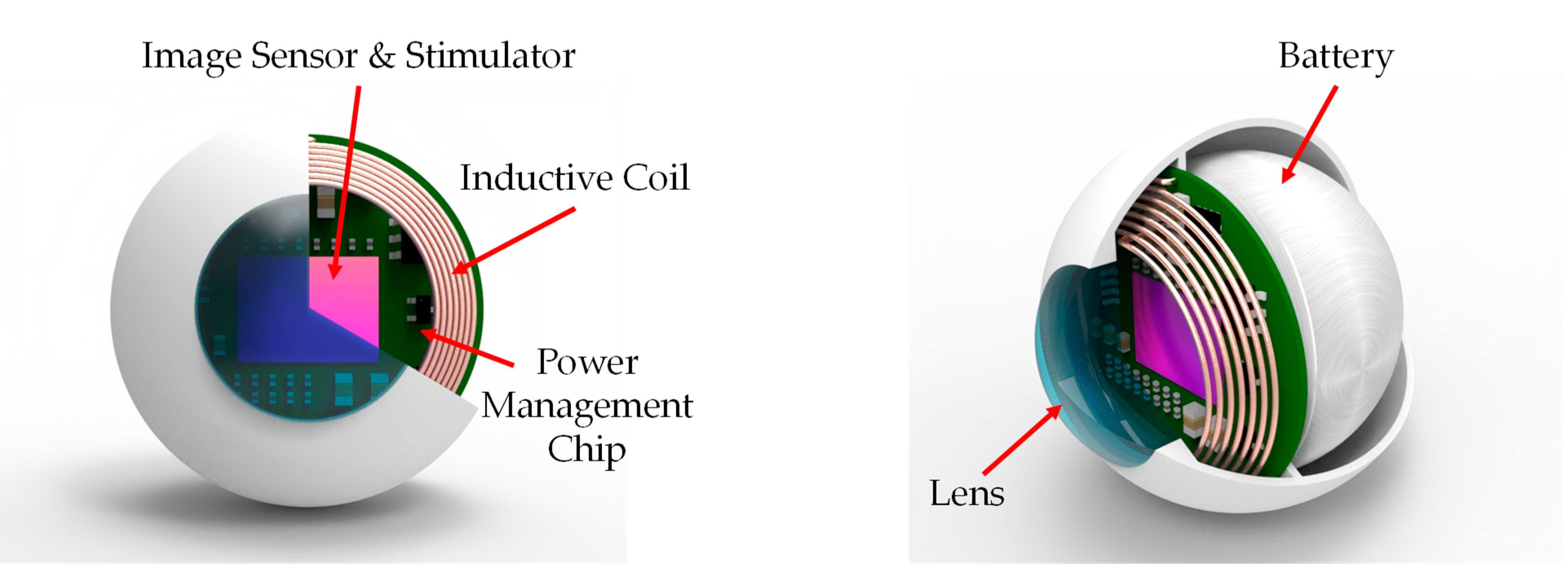
:1. Introduction
2. Materials
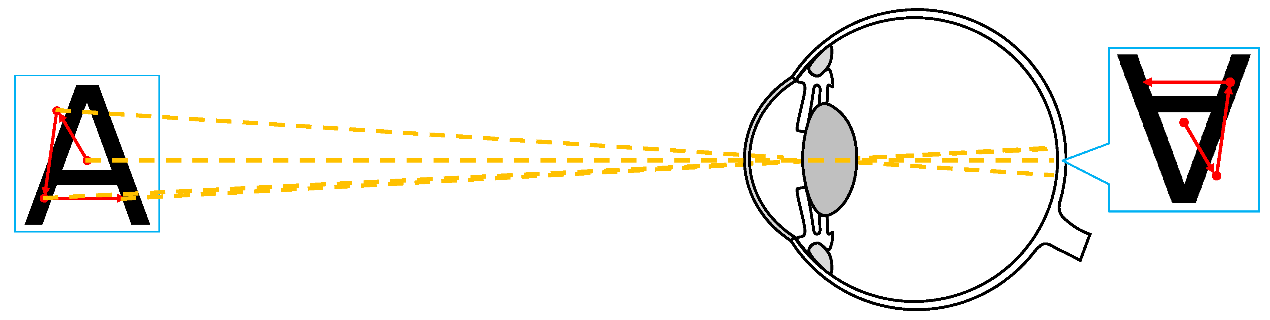
2.1. Behavioral Model of Biological Eye
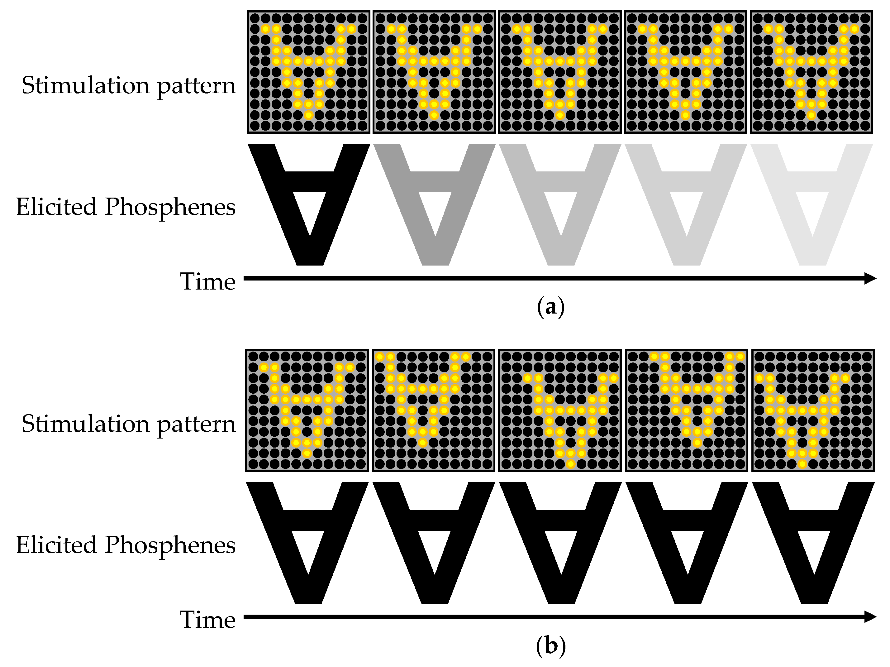
2.2. Implementation of Electronic Microsaccade Circuit
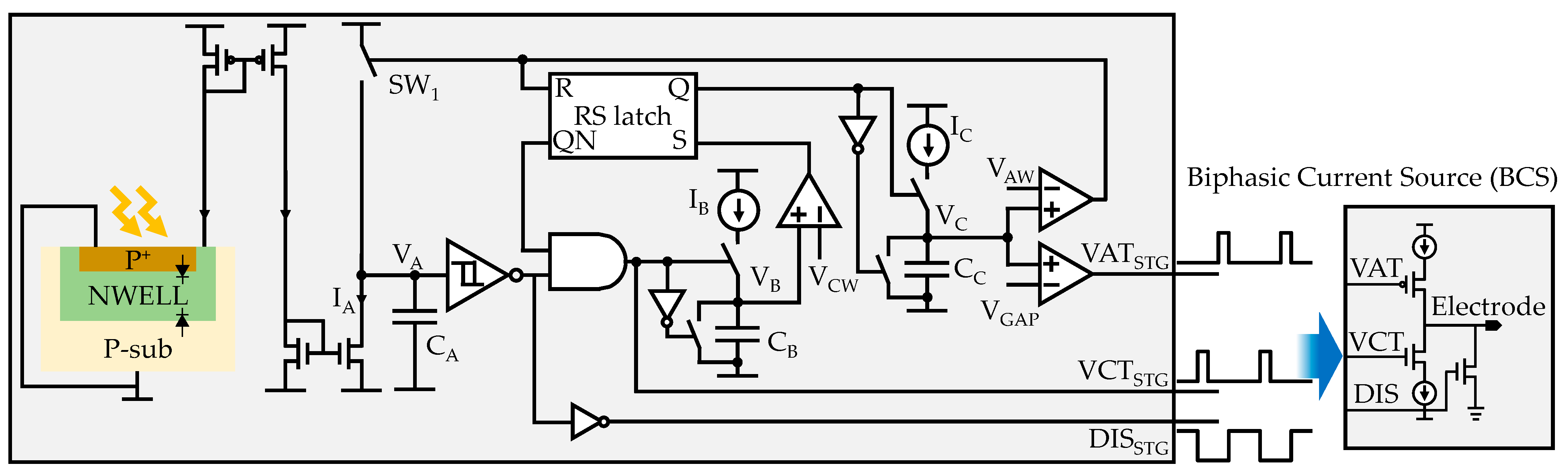
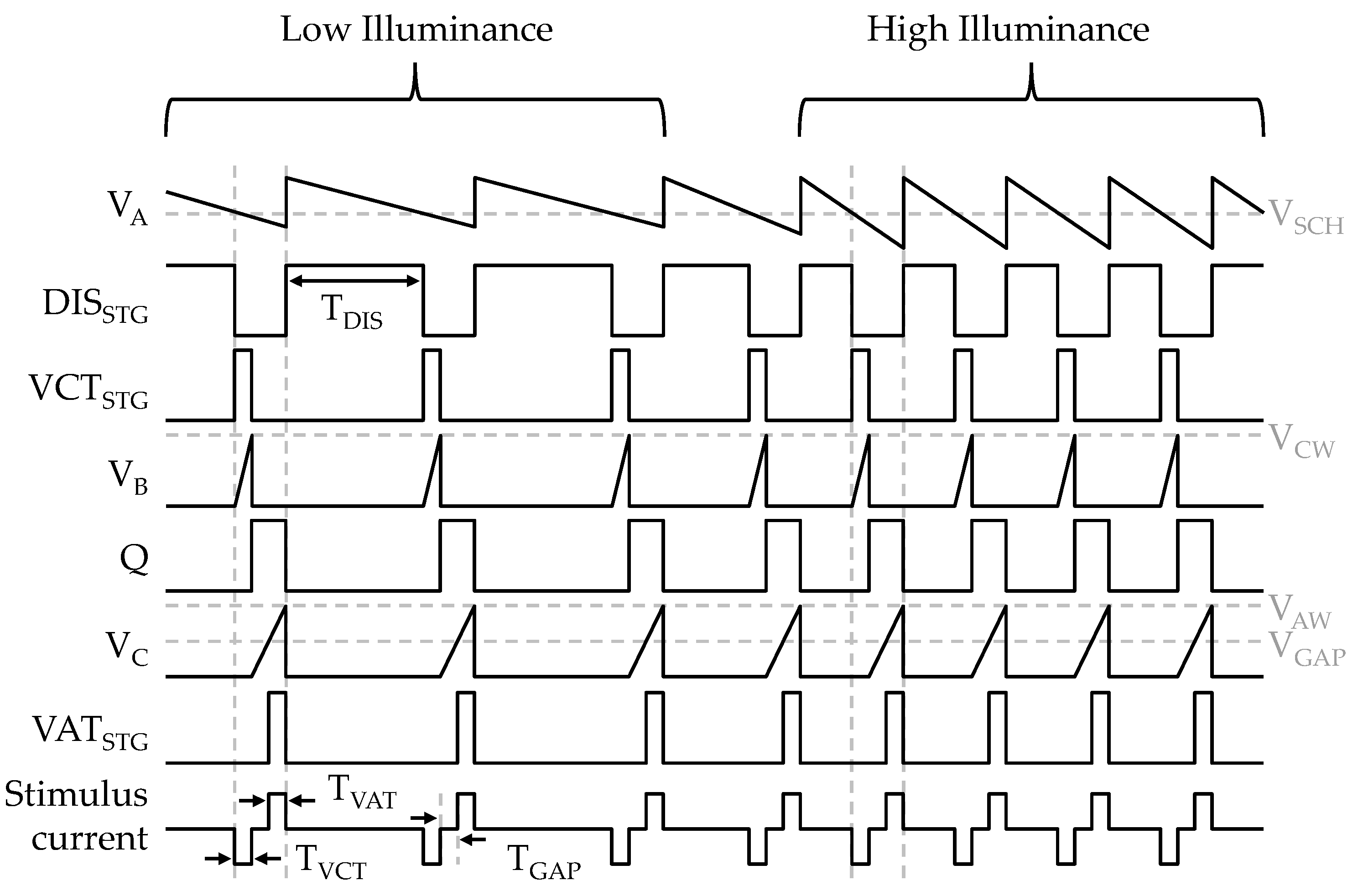
2.2.1. Light-to-Frequency Modulation
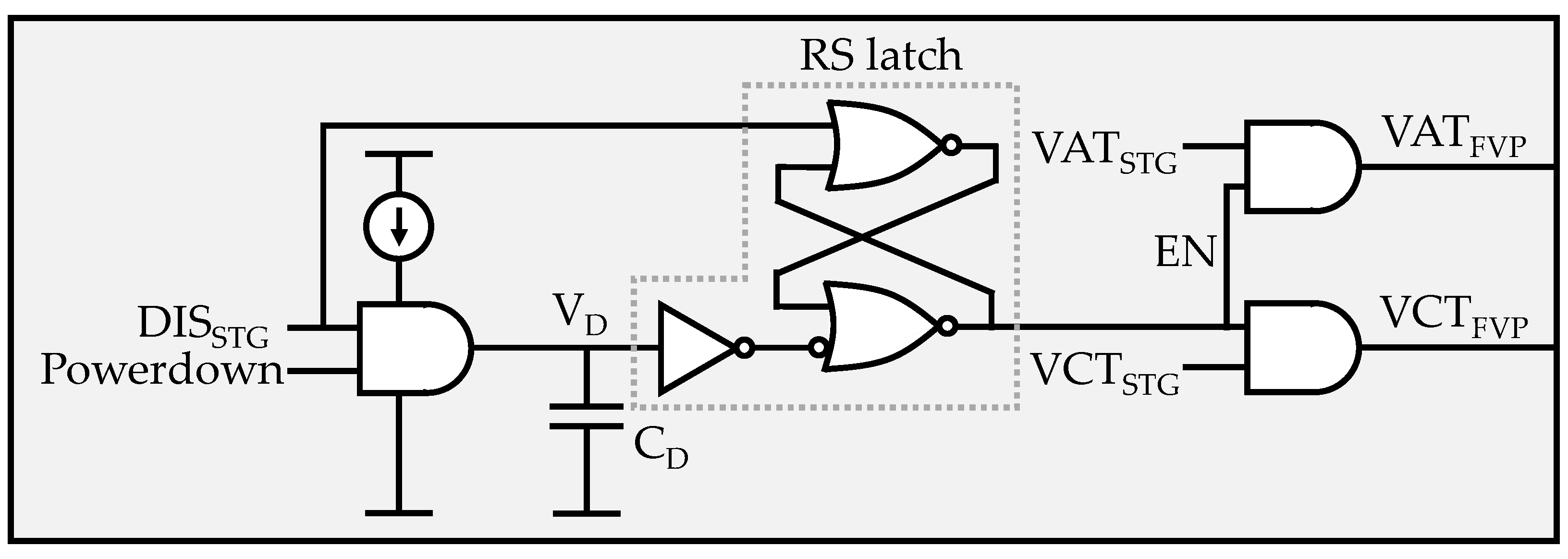
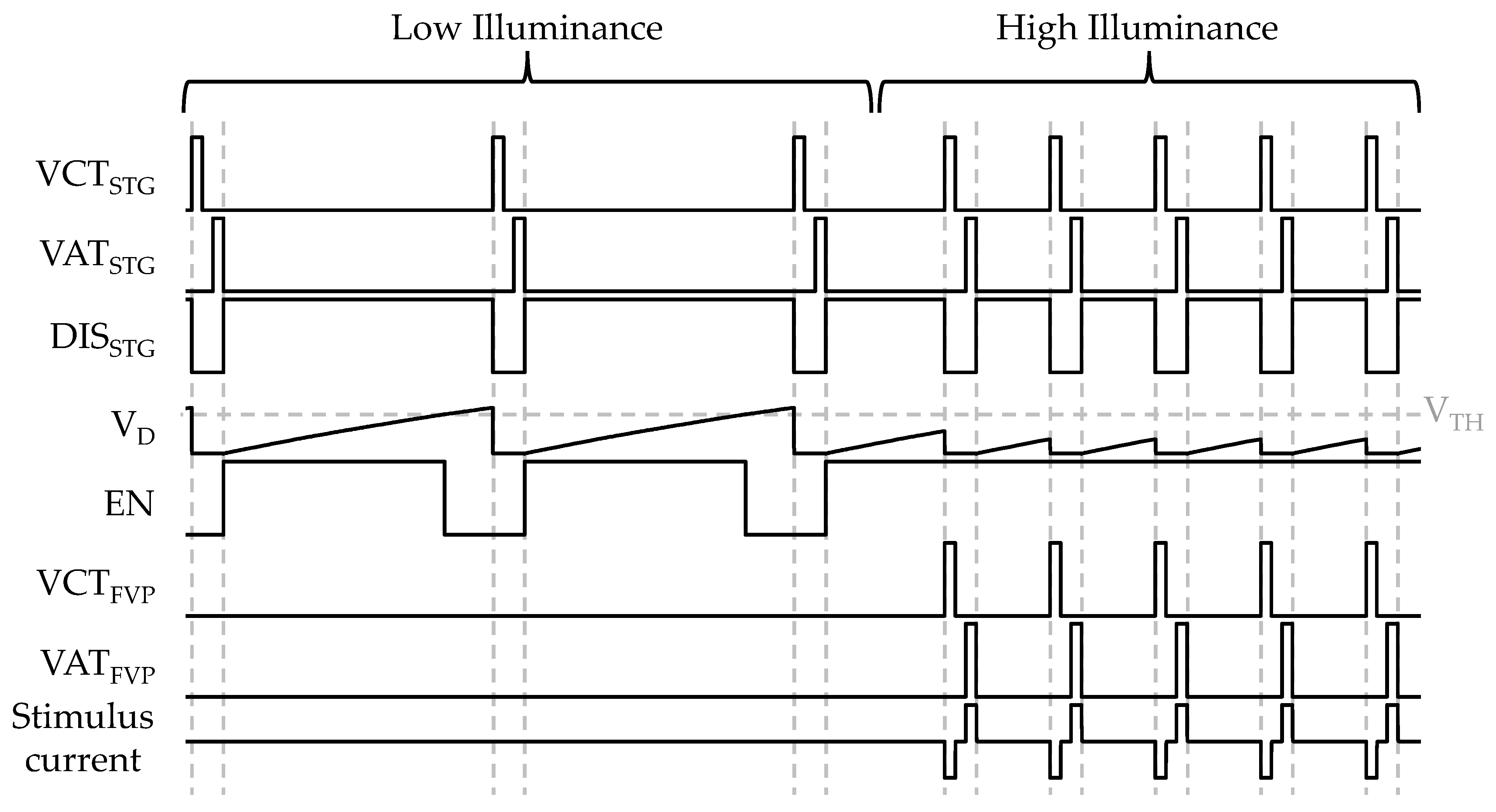
2.2.2. Flicker Vision Prevention Circuit
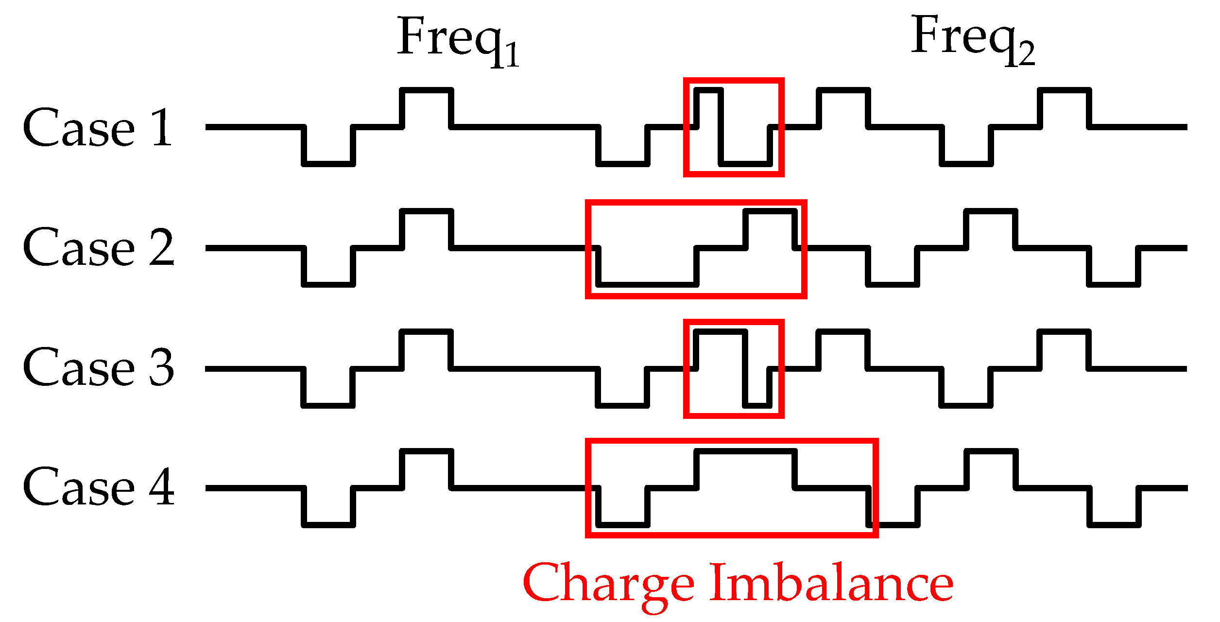
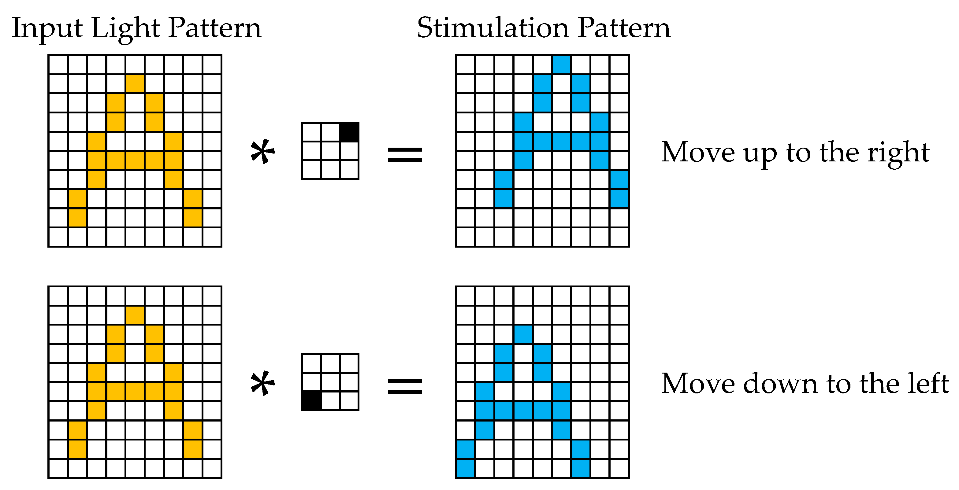
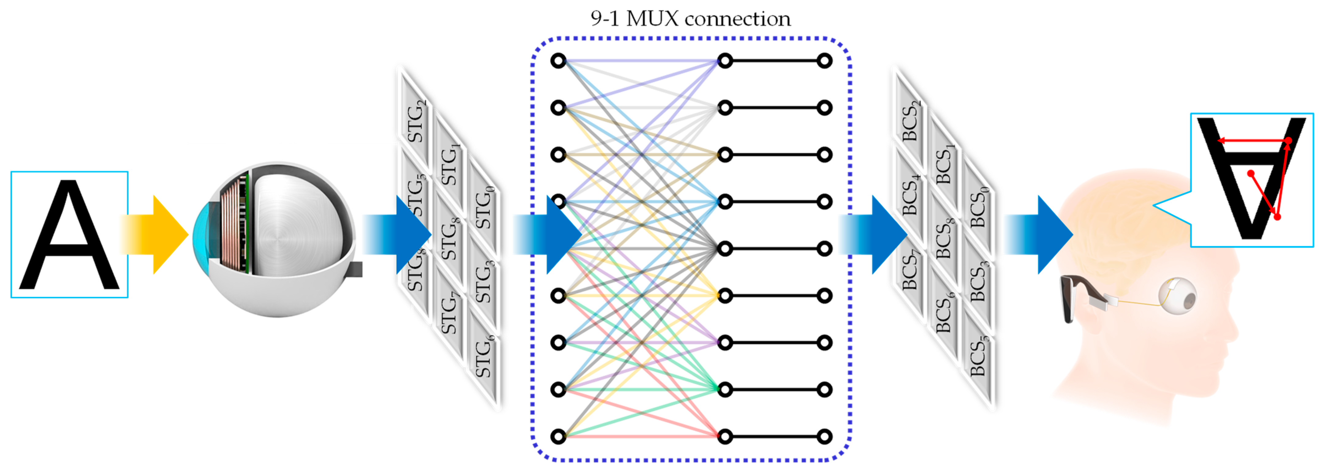
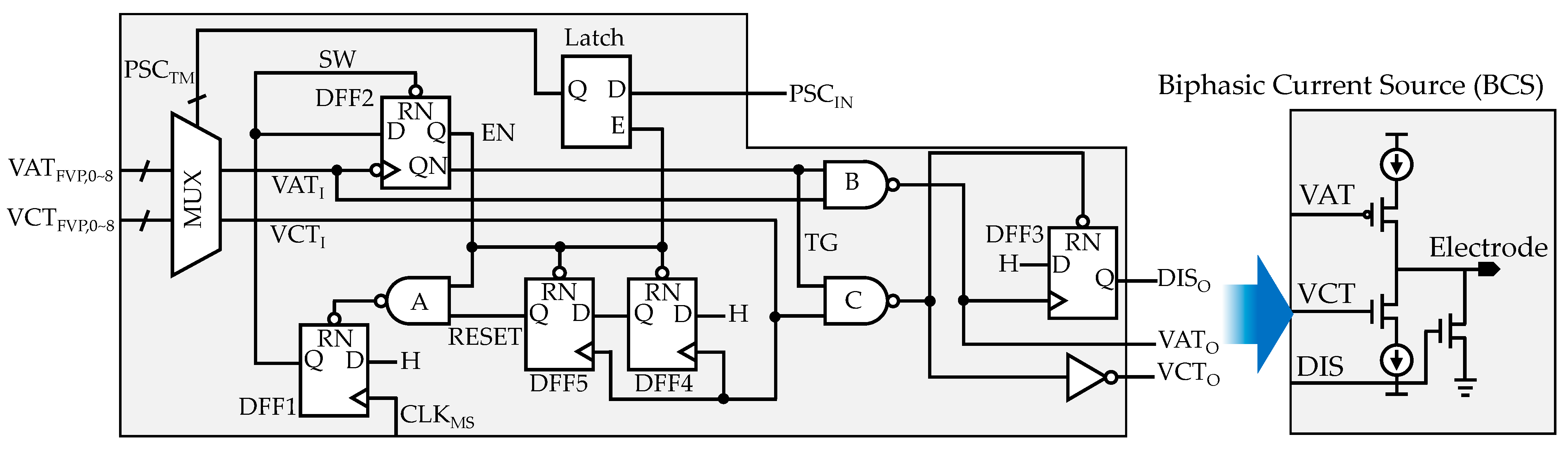
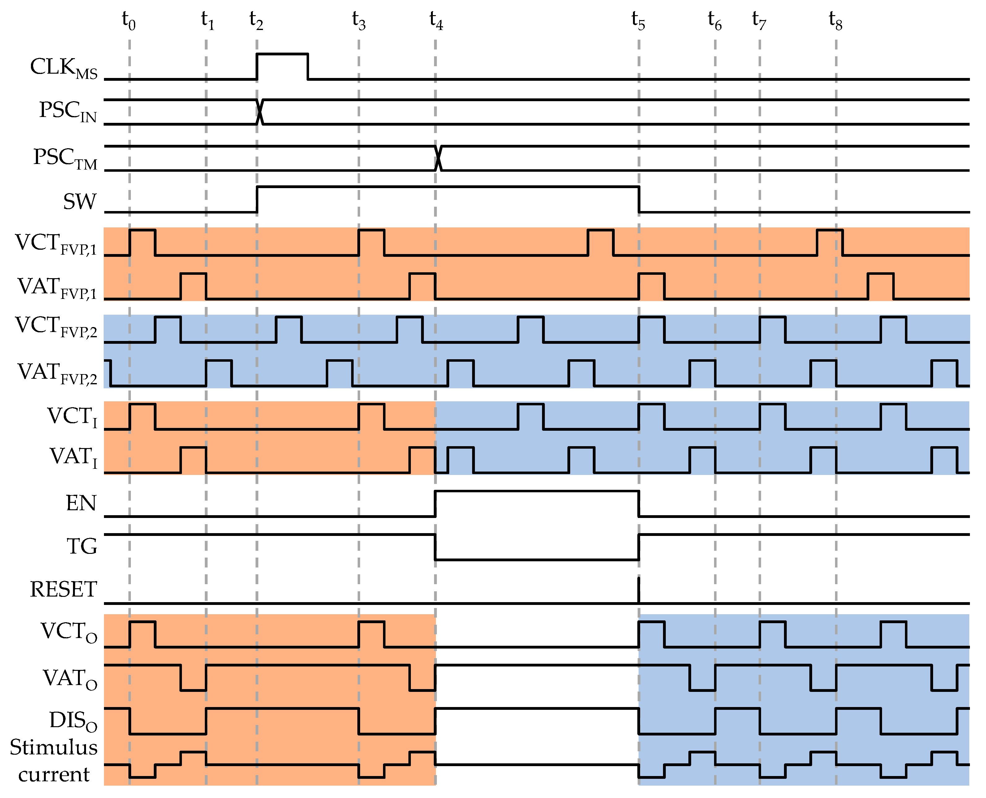
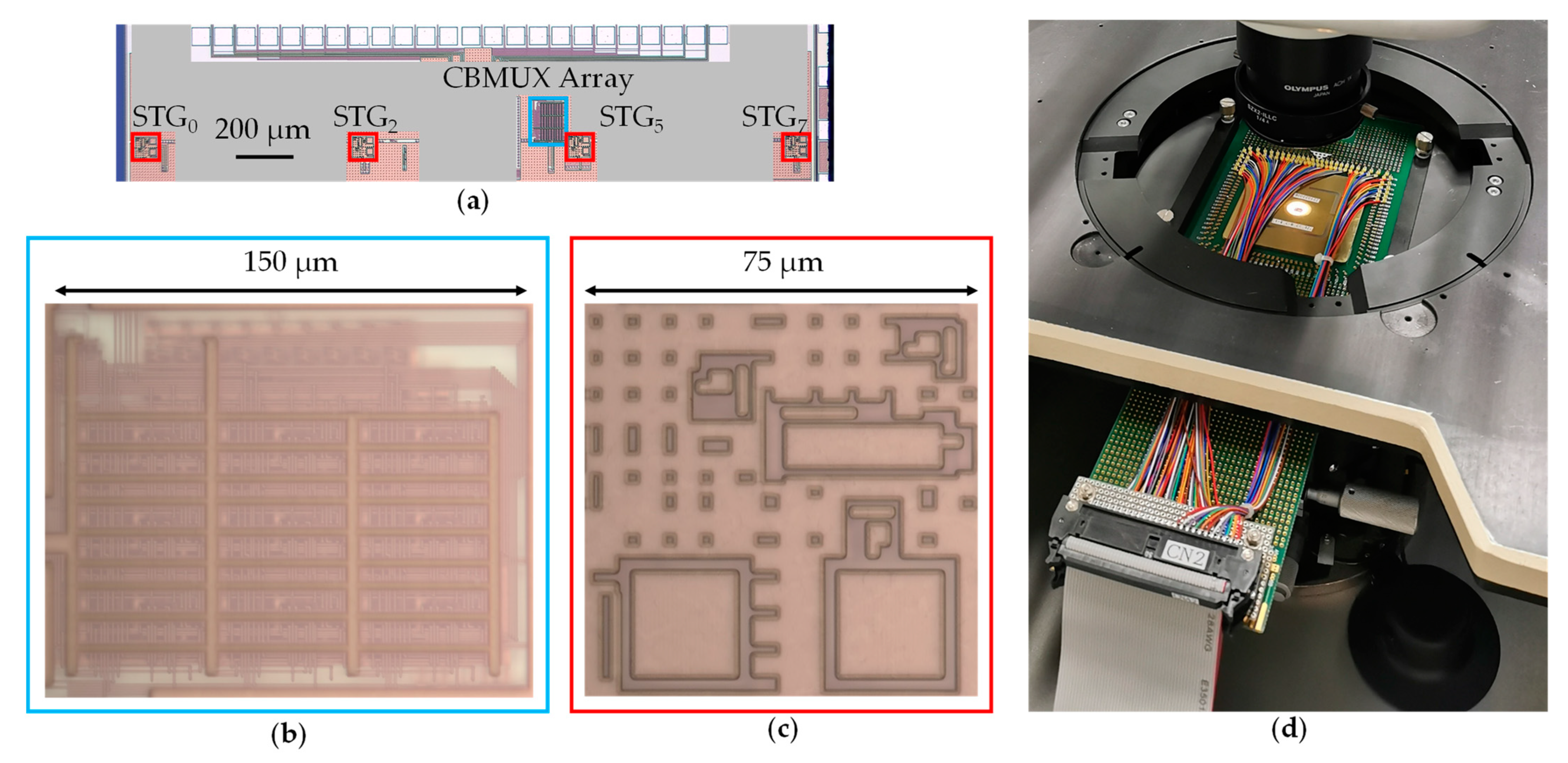
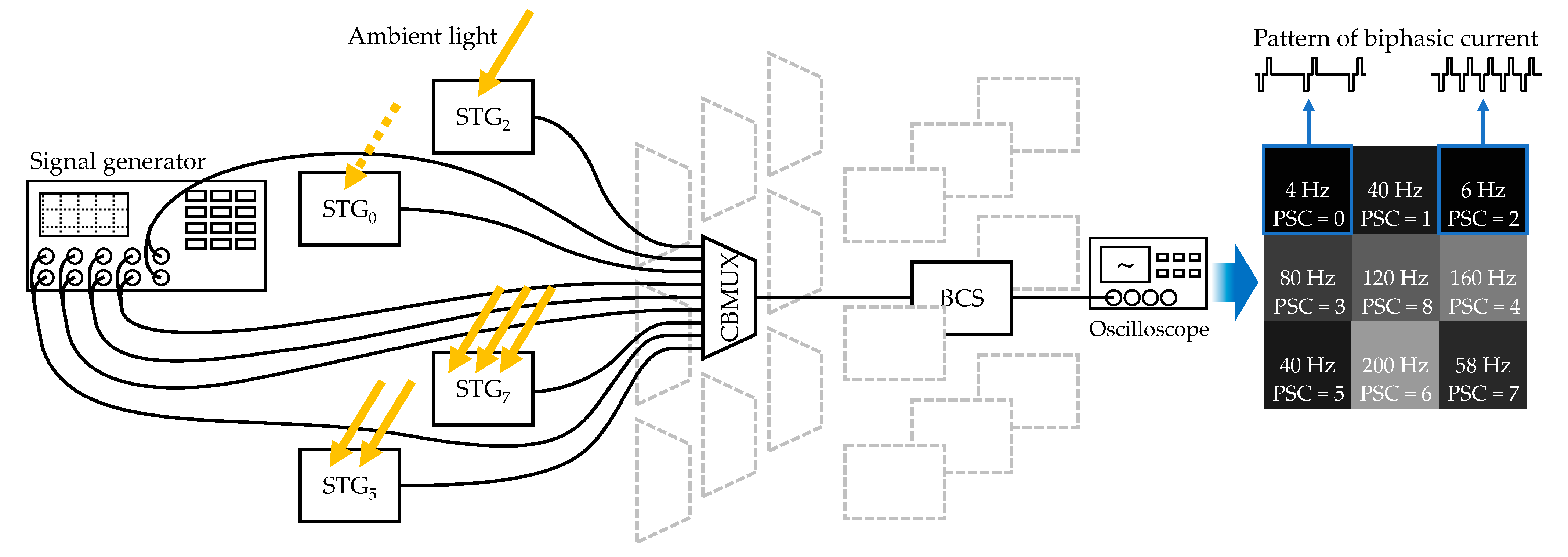
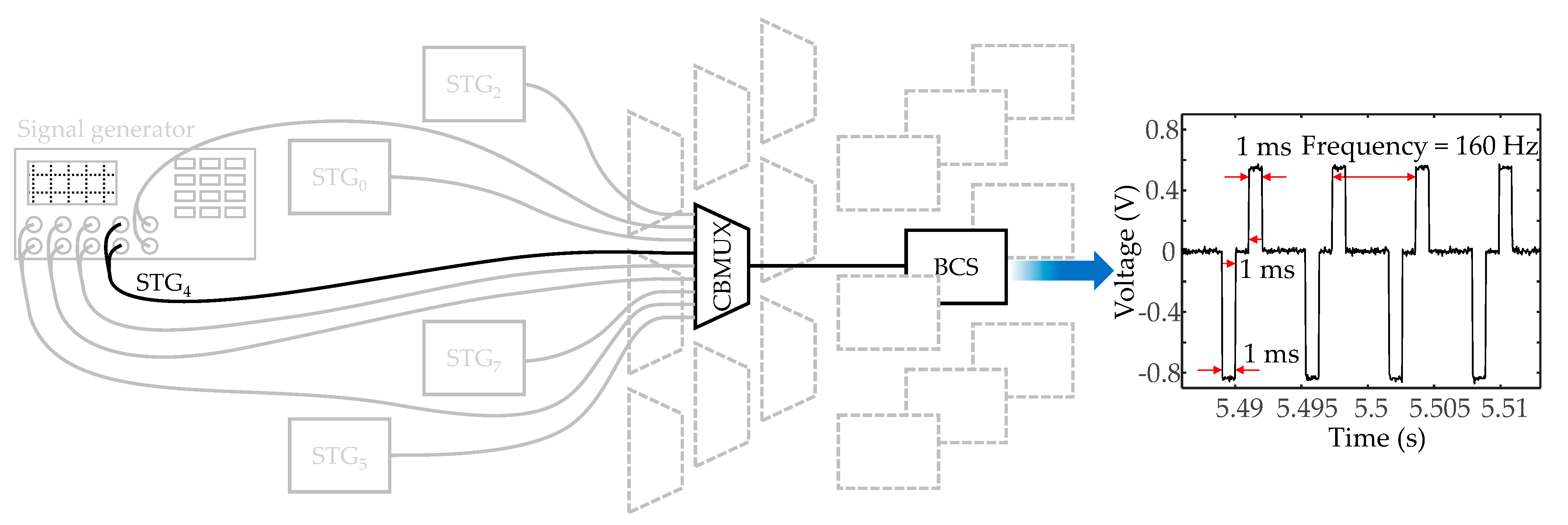
2.2.3. Charge-Balancing Multiplexer for Safe Electronic Microsaccade
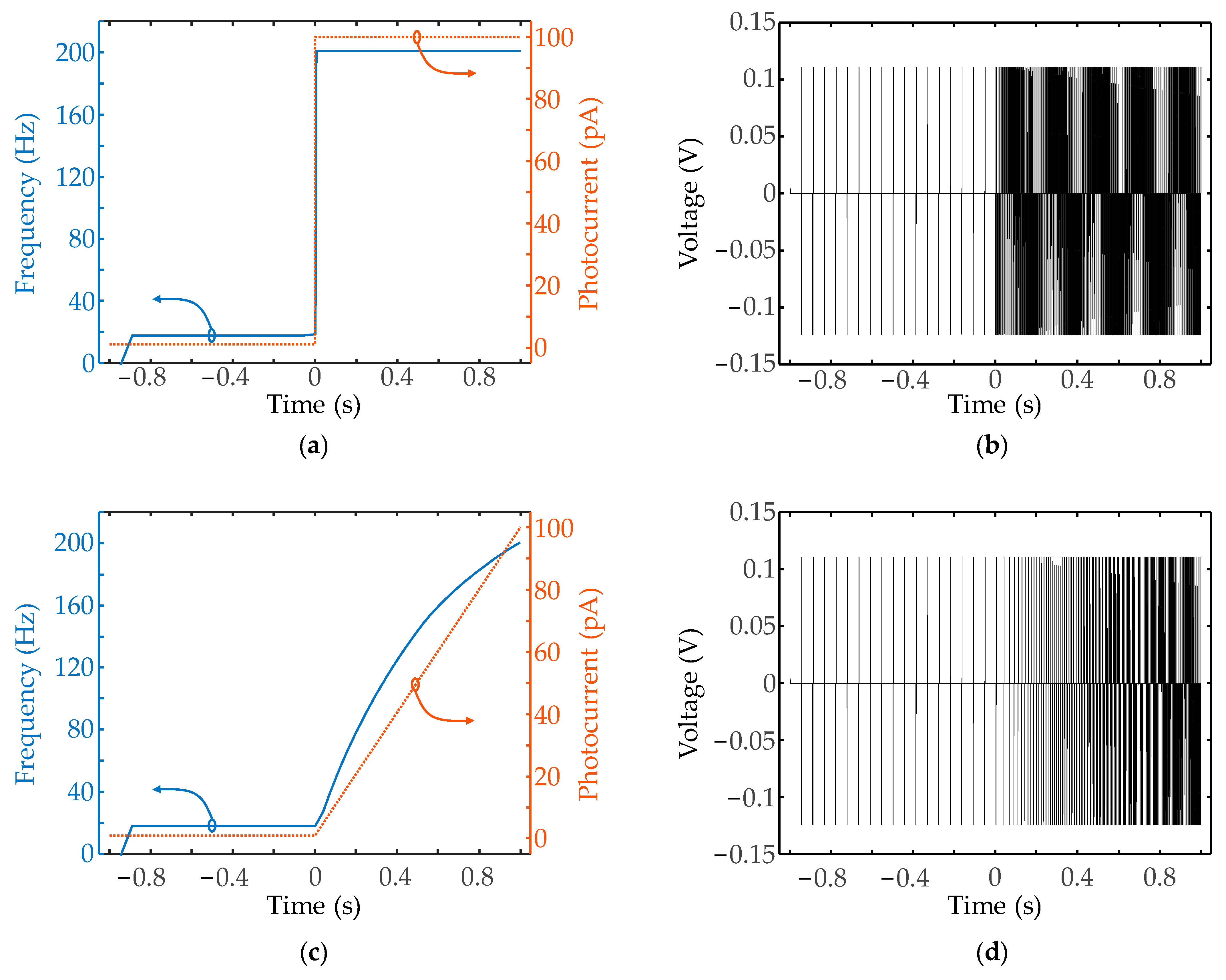
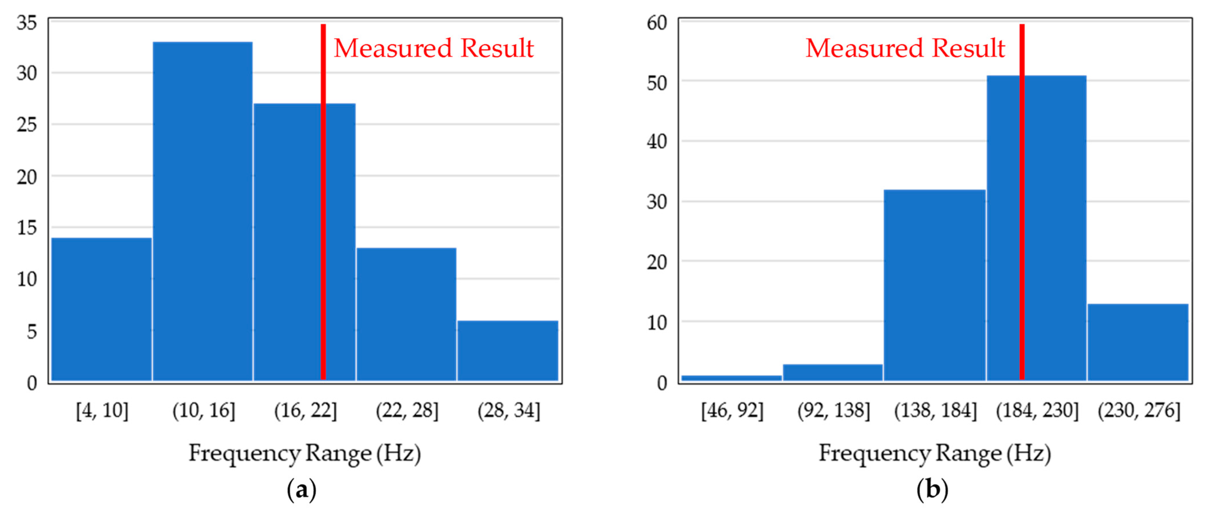
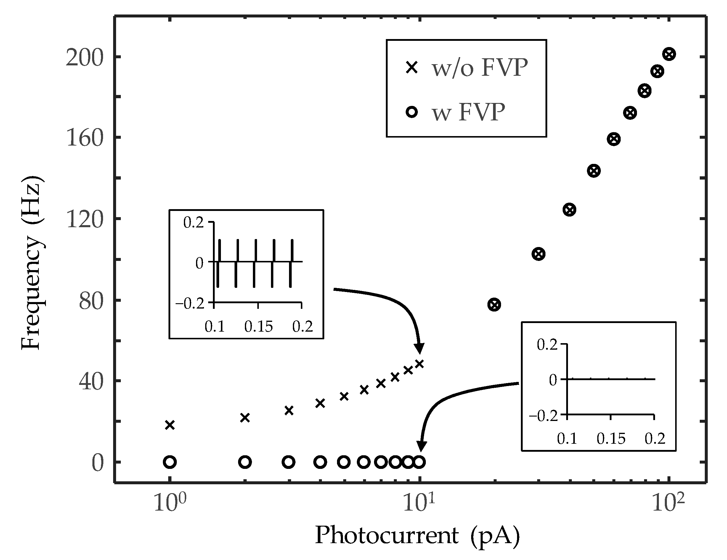
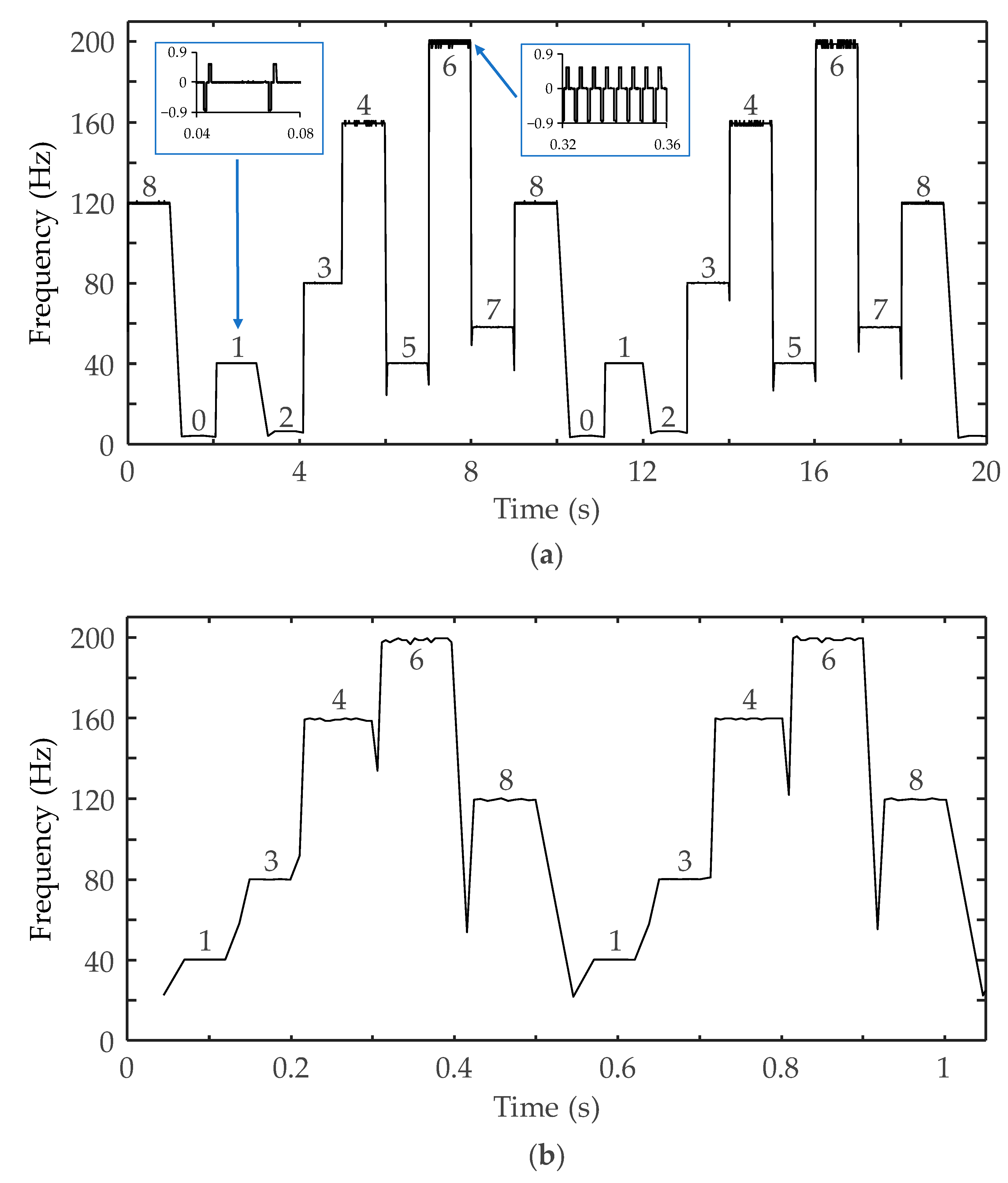
3. Results
4. Discussion
5. Conclusions
Author Contributions
Funding
Data Availability Statement
Acknowledgments
Conflicts of Interest
References
- Bourne, R.; Steinmetz, J.D.; Flaxman, S.; Briant, P.S.; Taylor, H.R.; Resnikoff, S.; Casson, R.J.; Abdoli, A.; Abu-Gharbieh, E.; Afshin, A.; et al. Trends in Prevalence of Blindness and Distance and near Vision Impairment over 30 Years: An Analysis for the Global Burden of Disease Study. Lancet Glob. Health 2021, 9, e130–e143. [Google Scholar] [CrossRef]
- Zrenner, E. Fighting Blindness with Microelectronics. Sci. Transl. Med. 2013, 5, 210ps16. [Google Scholar] [CrossRef]
- Weiland, J.D.; Humayun, M.S. Retinal Prosthesis. IEEE Trans. Biomed. Eng. 2014, 61, 1412–1424. [Google Scholar] [CrossRef] [Green Version]
- Ong, J.M.; da Cruz, L. The Bionic Eye: A Review. Clin. Experiment. Ophthalmol. 2012, 40, 6–17. [Google Scholar] [CrossRef]
- Chuang, A.T.; Margo, C.E.; Greenberg, P.B. Retinal Implants: A Systematic Review. Br. J. Ophthalmol. 2014, 98, 852–856. [Google Scholar] [CrossRef]
- Hammes, H.-P.; Feng, Y.; Pfister, F.; Brownlee, M. Diabetic Retinopathy: Targeting Vasoregression. Diabetes 2011, 60, 9–16. [Google Scholar] [CrossRef] [Green Version]
- El-Danaf, R.N.; Huberman, A.D. Characteristic Patterns of Dendritic Remodeling in Early-Stage Glaucoma: Evidence from Genetically Identified Retinal Ganglion Cell Types. J. Neurosci. 2015, 35, 2329–2343. [Google Scholar] [CrossRef] [PubMed] [Green Version]
- Gu, L.; Poddar, S.; Lin, Y.; Long, Z.; Zhang, D.; Zhang, Q.; Shu, L.; Qiu, X.; Kam, M.; Javey, A.; et al. A Biomimetic Eye with a Hemispherical Perovskite Nanowire Array Retina. Nature 2020, 581, 278–282. [Google Scholar] [CrossRef]
- Dobelle, W.H. Artificial Vision for the Blind by Connecting a Television Camera to the Visual Cortex. ASAIO J. 2000, 46, 3–9. [Google Scholar] [CrossRef] [Green Version]
- Rush, A.D.; Troyk, P.R. A Power and Data Link for a Wireless-Implanted Neural Recording System. IEEE Trans. Biomed. Eng. 2012, 59, 3255–3262. [Google Scholar] [CrossRef]
- Tomioka, K.; Toyoda, K.; Ishizaki, T.; Noda, T.; Ohta, J.; Kimura, M. Retinal Prosthesis Using Thin-Film Devices on a Transparent Substrate and Wireless Power Transfer. IEEE Trans. Electron. Devices 2020, 67, 529–534. [Google Scholar] [CrossRef]
- Wu, C.-Y.; Tseng, C.-K.; Liao, J.-H.; Chiao, C.-C.; Chu, F.-L.; Tsai, Y.-C.; Ohta, J.; Noda, T. CMOS 256-Pixel/480-Pixel Photovoltaic-Powered Subretinal Prosthetic Chips with Wide Image Dynamic Range and Bi/Four-Directional Sharing Electrodes and Their Ex Vivo Experimental Validations with Mice. IEEE Trans. Circuits Syst. Regul. Pap. 2020, 67, 3273–3283. [Google Scholar] [CrossRef]
- Lemaire, W.; Benhouria, M.; Koua, K.; Besrour, M.; Gauthier, L.-P.; Martin-Hardy, G.; Rossignol, T.; Roy, S.; Fontaine, R. Retinal Stimulator ASIC Architecture Based on a Joint Power and Data Optical Link. IEEE J. Solid-State Circuits 2021, 56, 2158–2170. [Google Scholar] [CrossRef]
- Kelly, S.K.; Shire, D.B.; Chen, J.; Doyle, P.; Gingerich, M.D.; Cogan, S.F.; Drohan, W.A.; Behan, S.; Theogarajan, L.; Wyatt, J.L.; et al. A Hermetic Wireless Subretinal Neurostimulator for Vision Prostheses. IEEE Trans. Biomed. Eng. 2011, 58, 3197–3205. [Google Scholar] [CrossRef] [Green Version]
- Martinez-Conde, S.; Macknik, S.L.; Hubel, D.H. The Role of Fixational Eye Movements in Visual Perception. Nat. Rev. Neurosci. 2004, 5, 229–240. [Google Scholar] [CrossRef]
- Hafed, Z.M.; Goffart, L.; Krauzlis, R.J. A Neural Mechanism for Microsaccade Generation in the Primate Superior Colliculus. Science 2009, 323, 940–943. [Google Scholar] [CrossRef] [Green Version]
- Dimigen, O.; Valsecchi, M.; Sommer, W.; Kliegl, R. Human Microsaccade-Related Visual Brain Responses. J. Neurosci. 2009, 29, 12321–12331. [Google Scholar] [CrossRef] [Green Version]
- Collewijn, H.; Kowler, E. The Significance of Microsaccades for Vision and Oculomotor Control. J. Vis. 2008, 8, 20. [Google Scholar] [CrossRef]
- Kowler, E. Eye Movements: The Past 25years. Vision Res. 2011, 51, 1457–1483. [Google Scholar] [CrossRef] [Green Version]
- Stronks, H.C.; Dagnelie, G. The Functional Performance of the Argus II Retinal Prosthesis. Expert Rev. Med. Devices 2014, 11, 23–30. [Google Scholar] [CrossRef] [Green Version]
- Singh, P.R.; Liu, W.; Sivaprakasam, M.; Humayun, M.S.; Weiland, J.D. A Matched Biphasic Microstimulator for an Implantable Retinal Prosthetic Device. In Proceedings of the 2004 IEEE International Symposium on Circuits and Systems (ISCAS), Vancouver, BC, Canada, 23–26 May 2004; Volume 4, p. IV–1. [Google Scholar]
- Sivaprakasam, M.; Liu, W.; Humayun, M.S.; Weiland, J.D. A Variable Range Bi-Phasic Current Stimulus Driver Circuitry for an Implantable Retinal Prosthetic Device. IEEE J. Solid-State Circuits 2005, 40, 763–771. [Google Scholar] [CrossRef]
- Sivaprakasam, M.; Liu, W.; Wang, G.; Weiland, J.D.; Humayun, M.S. Architecture Tradeoffs in High-Density Microstimulators for Retinal Prosthesis. IEEE Trans. Circuits Syst. Regul. Pap. 2005, 52, 2629–2641. [Google Scholar] [CrossRef]
- Palanker, D.; Le Mer, Y.; Mohand-Said, S.; Muqit, M.; Sahel, J.A. Photovoltaic Restoration of Central Vision in Atrophic Age-Related Macular Degeneration. Ophthalmology 2020, 127, 1097–1104. [Google Scholar] [CrossRef]
- Liu, W.; Hurnayun, M.S. Retinal Prosthesis. In Proceedings of the 2004 IEEE International Solid-State Circuits Conference (IEEE Cat. No.04CH37519), San Francisco, CA, USA, 15–19 February 2004; Volume 1, pp. 218–219. [Google Scholar]
- Horsager, A.; Greenberg, R.J.; Fine, I. Spatiotemporal Interactions in Retinal Prosthesis Subjects. Investig. Ophthalmol. Vis. Sci. 2010, 51, 1223–1233. [Google Scholar] [CrossRef] [Green Version]
- Eisen-Enosh, A.; Farah, N.; Burgansky-Eliash, Z.; Polat, U.; Mandel, Y. Evaluation of Critical Flicker-Fusion Frequency Measurement Methods for the Investigation of Visual Temporal Resolution. Sci. Rep. 2017, 7, 15621. [Google Scholar] [CrossRef] [Green Version]
- Shimokawa, K.; Qian, Z.; Takezawa, Y.; Kino, H.; Fukushima, T.; Kiyoyama, K.; Tanaka, T. Experimental Evaluation of Stimulus Current Generator with Laplacian Edge-Enhancement for 3-D Stacked Retinal Prosthesis Chip. In Proceedings of the 2017 IEEE Biomedical Circuits and Systems Conference (BioCAS), Turin, Italy, 19–21 October 2017; pp. 1–4. [Google Scholar]
- Liang, Y.; Qian, Z.; Du, B.; Ye, J.; Nakamura, K.; Wang, S.; Kino, H.; Fukushima, T.; Kiyoyama, K.; Tanaka, T. Design and Evaluation of Electronic-Microsaccade with Balanced Stimulation for Artificial Vision System. In Proceedings of the 2021 IEEE Biomedical Circuits and Systems Conference (BioCAS), Berlin, Germany, 7–9 October 2021; pp. 01–04. [Google Scholar]
- Martinez-Conde, S.; Macknik, S.L.; Troncoso, X.G.; Dyar, T.A. Microsaccades Counteract Visual Fading during Fixation. Neuron 2006, 49, 297–305. [Google Scholar] [CrossRef] [Green Version]
- Rolfs, M. Microsaccades: Small Steps on a Long Way. Vision Res. 2009, 49, 2415–2441. [Google Scholar] [CrossRef] [Green Version]
- Naganuma, H.; Kiyoyama, K.; Tanaka, T. A 37 × 37 Pixels Artificial Retina Chip with Edge Enhancement Function for 3-D Stacked Fully Implantable Retinal Prosthesis. In Proceedings of the 2012 IEEE Biomedical Circuits and Systems Conference (BioCAS), Hsinchu, Taiwan, 28–30 November 2012; pp. 212–215. [Google Scholar]
- Bekerman, I.; Gottlieb, P.; Vaiman, M. Variations in Eyeball Diameters of the Healthy Adults. J. Ophthalmol. 2014, 2014, 503645. [Google Scholar] [CrossRef] [Green Version]
- Pérez Fornos, A.; Sommerhalder, J.; da Cruz, L.; Sahel, J.A.; Mohand-Said, S.; Hafezi, F.; Pelizzone, M. Temporal Properties of Visual Perception on Electrical Stimulation of the Retina. Investig. Ophthalmol. Vis. Sci. 2012, 53, 2720–2731. [Google Scholar] [CrossRef] [Green Version]
- Asher, A.; Segal, W.A.; Baccus, S.A.; Yaroslavsky, L.P.; Palanker, D.V. Image Processing for a High-Resolution Optoelectronic Retinal Prosthesis. IEEE Trans. Biomed. Eng. 2007, 54, 993–1004. [Google Scholar] [CrossRef]
- Weitz, A.C.; Behrend, M.R.; Ahuja, A.K.; Christopher, P.; Wei, J.; Wuyyuru, V.; Patel, U.; Greenberg, R.J.; Humayun, M.S.; Chow, R.H.; et al. Interphase Gap as a Means to Reduce Electrical Stimulation Thresholds for Epiretinal Prostheses. J. Neural Eng. 2014, 11, 016007. [Google Scholar] [CrossRef] [Green Version]
- Carlyon, R.P.; van Wieringen, A.; Deeks, J.M.; Long, C.J.; Lyzenga, J.; Wouters, J. Effect of Inter-Phase Gap on the Sensitivity of Cochlear Implant Users to Electrical Stimulation. Hear. Res. 2005, 205, 210–224. [Google Scholar] [CrossRef]
- John, S.E.; Shivdasani, M.N.; Williams, C.E.; Morley, J.W.; Shepherd, R.K.; Rathbone, G.D.; Fallon, J.B. Suprachoroidal Electrical Stimulation: Effects of Stimulus Pulse Parameters on Visual Cortical Responses. J. Neural Eng. 2013, 10, 056011. [Google Scholar] [CrossRef]


| PSC (BCD Code) | Signal Path from STG to BSC |
|---|---|
| 0 | VAT and VCT from the upper-left STG |
| 1 | VAT and VCT from the upper-center STG |
| 2 | VAT and VCT the upper-right STG |
| 3 | VAT and VCT from the middle-left STG |
| 4 | VAT and VCT from the middle-right STG |
| 5 | VAT and VCT from the lower-left STG |
| 6 | VAT and VCT from the lower-center STG |
| 7 | VAT and VCT from the lower-right STG |
| 8 | VAT and VCT from the central STG |
| ≥9 | N/A |
| Process | 0.18 μm Standard CMOS 1P6M |
|---|---|
| Power Supply | 1.8 V |
| Pixel Count | 3 × 3 |
| STG Pixel Size | 75 × 75 μm2 (Including FVP circuit) |
| CBMUX Pixel Size | 45 × 26 μm2 |
| Power Consumption | 8.255 μW/pixel @PRF = 100 Hz |
| Microsaccade Speed | 0.1 or 1 Hz |
| External Component | Decoupling Capacitors |
Disclaimer/Publisher’s Note: The statements, opinions and data contained in all publications are solely those of the individual author(s) and contributor(s) and not of MDPI and/or the editor(s). MDPI and/or the editor(s) disclaim responsibility for any injury to people or property resulting from any ideas, methods, instructions or products referred to in the content. |
© 2023 by the authors. Licensee MDPI, Basel, Switzerland. This article is an open access article distributed under the terms and conditions of the Creative Commons Attribution (CC BY) license (https://creativecommons.org/licenses/by/4.0/).
Share and Cite
Liang, Y.; Nakamura, K.; Du, B.; Wang, S.; Inoue, B.; Aruga, Y.; Kino, H.; Fukushima, T.; Kiyoyama, K.; Tanaka, T. An Electronic Microsaccade Circuit with Charge-Balanced Stimulation and Flicker Vision Prevention for an Artificial Eyeball System. Electronics 2023, 12, 2836. https://doi.org/10.3390/electronics12132836
Liang Y, Nakamura K, Du B, Wang S, Inoue B, Aruga Y, Kino H, Fukushima T, Kiyoyama K, Tanaka T. An Electronic Microsaccade Circuit with Charge-Balanced Stimulation and Flicker Vision Prevention for an Artificial Eyeball System. Electronics. 2023; 12(13):2836. https://doi.org/10.3390/electronics12132836
Chicago/Turabian StyleLiang, Yaogan, Kohei Nakamura, Bang Du, Shengwei Wang, Bunta Inoue, Yuta Aruga, Hisashi Kino, Takafumi Fukushima, Koji Kiyoyama, and Tetsu Tanaka. 2023. "An Electronic Microsaccade Circuit with Charge-Balanced Stimulation and Flicker Vision Prevention for an Artificial Eyeball System" Electronics 12, no. 13: 2836. https://doi.org/10.3390/electronics12132836