Resonant Hybrid Flyback, a New Topology for High Density Power Adaptors


1
Infineon Technologies AG, 85579 Munich, Germany
2
Pervasive Electronics Advanced Research Laboratory, Department of Electronics and Computer Technology, University of Granada, 18071 Granada, Spain
*
Author to whom correspondence should be addressed.
Electronics 2018, 7(12), 363; https://doi.org/10.3390/electronics7120363
Submission received: 1 November 2018
/
Revised: 20 November 2018
/
Accepted: 26 November 2018
/
Published: 1 December 2018
(This article belongs to the Section Power Electronics)
Abstract
:In this article, an innovative power adaptor based on the asymmetrical pulse width modulation (PWM) flyback topology will be presented. Its benefits compared to other state-of-the-art topologies, such as the active clamp flyback, are analyzed in detail. It will also describe the control methods to achieve high efficiency and power density using zero-voltage switching (ZVS) and zero-current switching (ZCS) techniques over the full range of the input voltage and the output load, providing comprehensive guidelines for the practical design. Finally, we demonstrate the convenience of the proposed design methods with a 65 W adaptor prototype achieving a peak efficiency of close to 95% and a minimum efficiency of 93.4% at full load over the range of the input voltage, as well as a world-class power density of 22 W/inch3 cased.
1. Introduction
In recent years, the amount of highly portable electronic devices—such as mobile phones, tablets, laptops, etc.—has increased significantly to satisfy social needs, communication needs, and enable access to a large variety of cloud-based services. Simultaneously, the need for power adaptors with high efficiency, to ensure minimal waste of energy, and minimally-sized electronic parts is highly desired to satisfy the portability premise [1].
Power adaptors must feature a wide input voltage range, typically ranging from 90 Vac to 264 Vac, and passive cooling. For low-power converters in which power factor correction is not required, flyback or flyback-based converters are preferably used due to their capability to handle a wide input to output voltage ratios [2,3]. Additionally, the potential for reducing the adaptor size is limited by the maximum losses that are generated at any given operating point. For a power adaptor where the heat is only dissipated passively, the maximum allowed surface temperature will determine the minimum allowed efficiency at full load and the minimum input voltage, which is typically the operating point characterized by a worst-case condition.
In a traditional flyback converter, the transformer acts as an energy storage element resulting in a larger transformer compared to forward topologies. This limits the maximum achievable power density. Over the years, increasing the switching frequency has been used to reduce the transformer size. Nevertheless, as the frequency increases, the energy losses in the parasitic elements—mainly transformer leakage inductance—and output metal-oxide-semiconductor field-effect transistor (MOSFET) capacitance become more significant. To overcome the issues related to higher switching frequencies, different variants of the flyback topology have become popular, all of which aim to recycle the energy of the parasitic elements, with the active clamp flyback being the most well-known variant in either complementary or non-complementary versions [4,5]. However, the original challenge related to the size of the transformer still remains: The energy to be transferred to the secondary side first has to be stored in the transformer.
In recent years, new transistor technologies allowing higher switching frequencies have become popular. Examples of these are silicon carbide and GaN MOSFETs [6,7,8]. The use of these new switches in active clamp flybacks seems to be able to solve both of the major limitations of high power density adaptors: Recycling energy from the parasitic elements while reducing the transformer size. Nevertheless, the higher switching frequencies are not exempt from problems. Faster switching frequencies raise a new challenge: To fulfill conductive or radiated electromagnetic interference (EMI) regulations, such as EN55022. Another limitation of this solution is the higher cost of special devices in a market where the total system cost is very sensitive.
The creatively titled asymmetrical duty cycle flyback converter is a hybrid between a flyback and a forward converter [9,10] that addresses the major problems related to high-density adaptors while using moderate switching frequencies. In this paper, a solution based on such a converter, and the control methods that ensure zero voltage switch (ZVS) and zero current switch (ZCS) over line and load will be presented.
2. Asymmetrical Duty Cycle Flyback
2.1. Topology
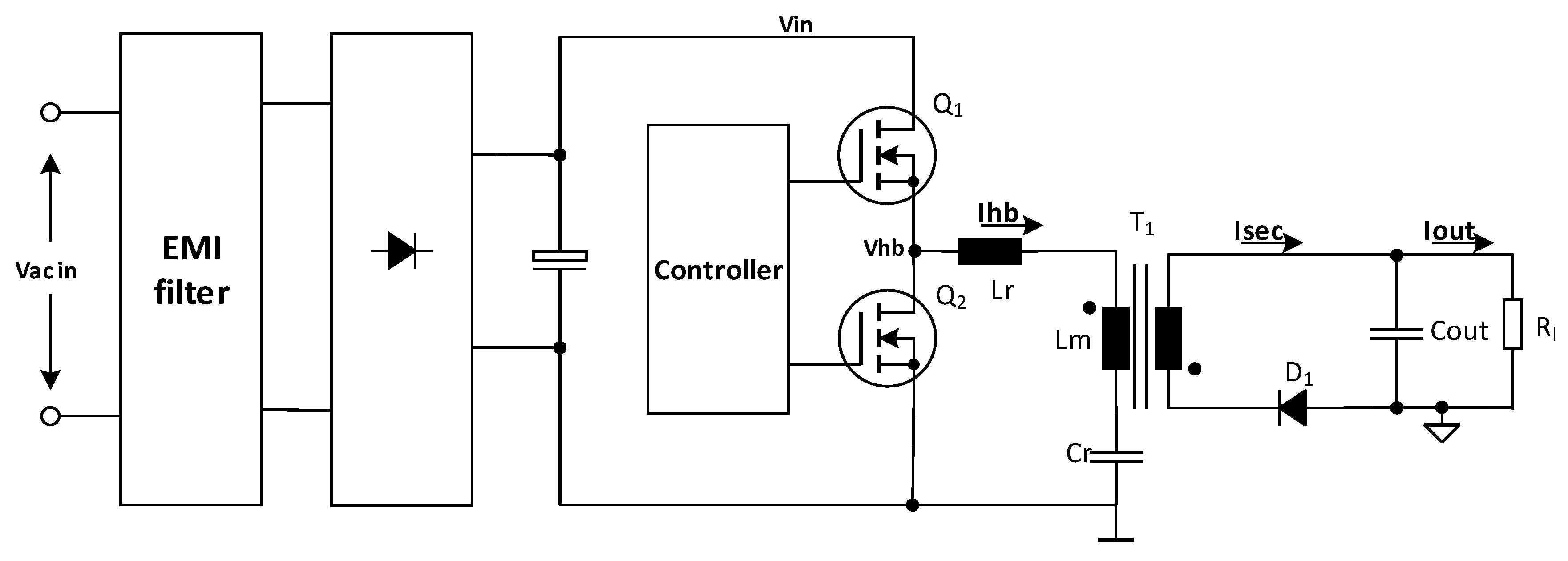
The general schematic of the asymmetrical duty cycle flyback converter is presented in Figure 1, including the elements needed in an adaptor, such as the EMI filter and the input rectifier [9]. It is important to note here the capacitor (Cr) is in series with the transformer, which is the major difference with respect to the traditional flyback and will make the converter behave as a hybrid flyback and a forward converter.
To achieve outstanding power density, a combination of the right topology, dimensioning, and advanced control techniques have to be used. In particular, the presented topology with the right control method can achieve ZVS and secondary ZCS under all conditions of input voltages and output current. Moreover, it recycles the energy of the transformer leakage inductance, which helps to reduce the losses and maximize efficiency. To further boost efficiency, synchronous rectification can be used in the secondary side.
The power circuit in the primary is realized by an LC tank driven by a half-bridge similar to an LLC converter. The resonant inductor Lr represents the series inductance, Lr being either the transformer leakage inductance or the leakage inductance plus an external inductor. It is worth mentioning that the converter can also be implemented by connecting the resonant capacitor Cr and the primary side of the power transformer between the positive node and the middle point of the half-bridge. This would result in a similar operation, but with the roles of the switch Q1 and Q2 inverted. A second resonant circuit is formed by Lr + Lm and Cr.
2.2. Resonant Operation Phases
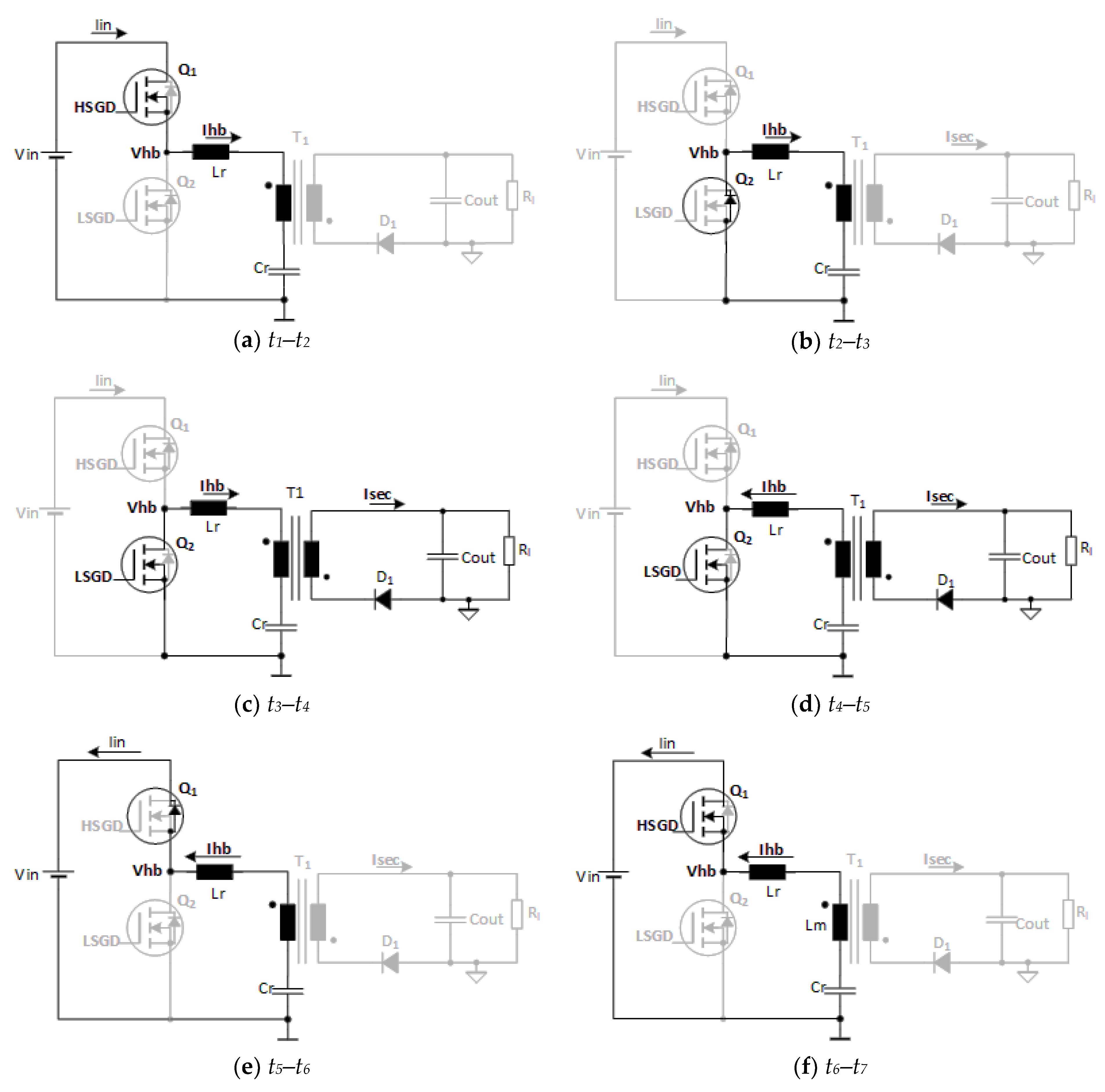
The operation phases of the resonant asymmetrical duty cycle flyback can be divided into six phases as schematized in Figure 2:
Phase 1, t1 to t2: During this phase, the Q1 switch is on and the Q2 switch is off. The current increases in the transformer and the voltage in the resonant capacitor Cr increases; both elements store energy. The secondary diode D1 is biased inversely hence no energy is transferred to the secondary side.
Phase 2, t2 to t3: In this phase, both switches Q1 and Q2 are off. The current in the transformer T1 will force the half-bridge middle point Vhb to drop until the body diode of Q2 MOSFET clamps the voltage. The primary side of the transformer now has the same voltage as the capacitor Cr.
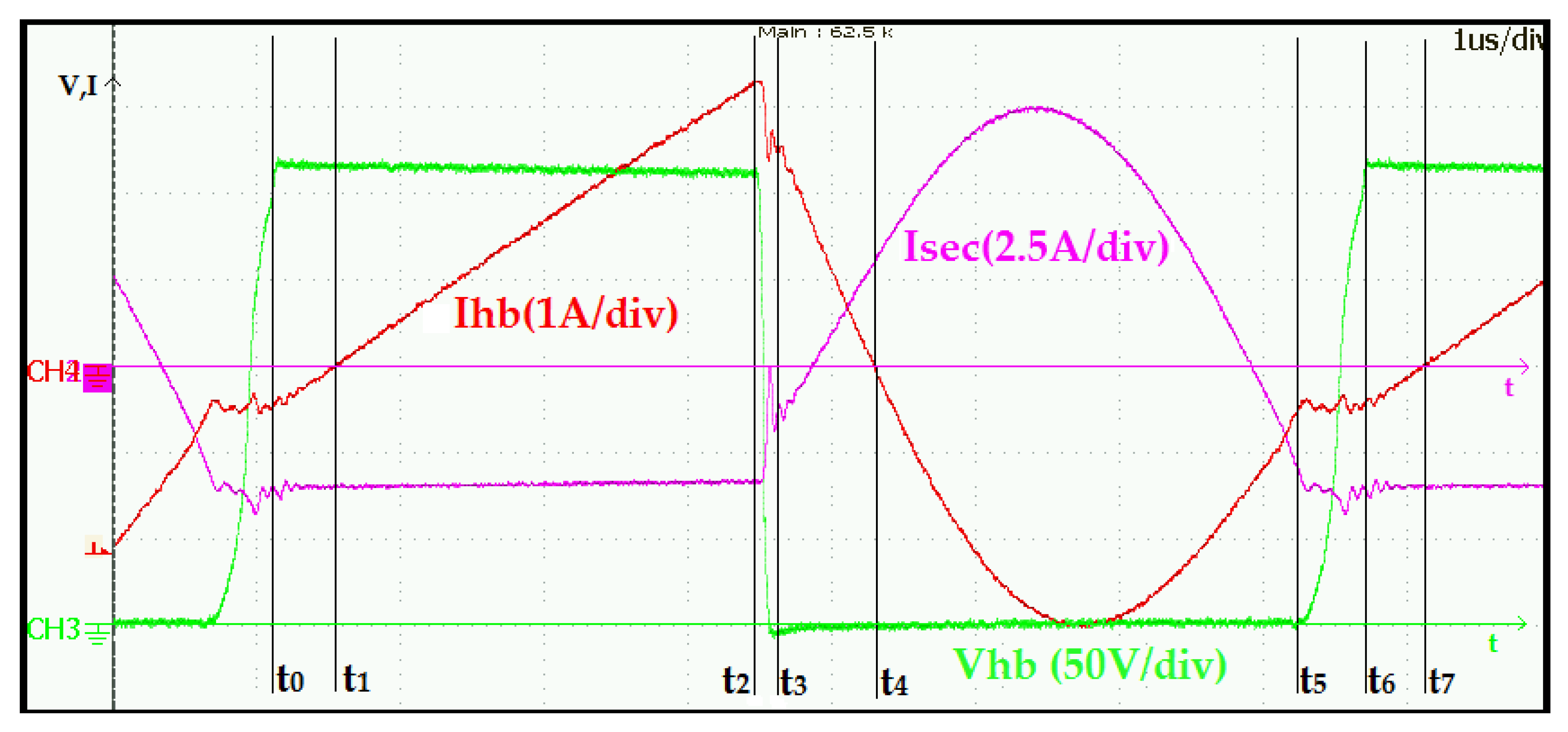
Phase 3, t3 to t4: During this phase the Q1 switch is off and Q2 is switched on under the ZVS condition; the secondary voltage is now equal to the voltage across the capacitor Cr divided by the turns ratio. The current starts flowing through D1 and the energy stored in the capacitor and the transformer is transferred to the output. Due to the LC tank formed by the Lr (transformer leakage inductance) and the resonant capacitor, the current in the secondary follows a sine wave with the period defined by the resonant frequency of those elements (see Figure 3). The current in the primary is the sum of the magnetizing current plus the reflected secondary current. The current in the resonant tank is still positive, mainly driven from the transformer T1 magnetizing inductance, and flows into the resonant capacitor Cr, charging it further.
Phase 4, t4 to t5: This phase is a continuation of the previous one. The Q1 switch is off and Q2 is switched on; the energy is still being transferred to the secondary side but the resonant tank current inverts its direction driven by the voltage in the resonant capacitor Cr. The energy of the resonant capacitor is not only transferred to the secondary side but also contributes to bringing the magnetizing current of the transformer T1 to a negative level as long as Q2 is on.
Phase 5, t5 to t6: In this phase, both switches Q1 and Q2 are off. The negative current induced in the transformer during the previous phase will force the half-bridge middle point Vhb to increase its voltage until it is clamped by the body diode of Q1.
Phase 6, t6 to t7: Similarly to phase 1, Q1 is switched on with the ZVS condition and Q2 is switched off, but the current in the transformer resonant tank is still negative, meaning that the excess of energy in the tank will be sent back to the input.
3. Asymmetrical Duty Cycle Flyback Control Methods
3.1. Duty Cycle and Output Voltage
Assuming negligible dead times, we can define the duty cycle as expressed by the Equation (1):
where TQ1 is the ON time of the Q1 switch and TQ2 is the ON time of the Q2 switch in Figure 1.
As described in detail in [11,12], the proposed topology provides an output voltage proportional to the duty cycle, according to:
where n represents the winding ratio between the primary and the secondary of the transformer.
Equation (2) shows that the output voltage is independent of the output current due to the fact that components without loss are assumed. However, in a real converter, it is necessary to compensate for energy losses in non-ideal components (i.e., capacitor ESR) and variations of the effective duty cycle due to the dead times.
3.2. Considerations for ZVS Operation
In order to achieve the ZVS condition before the MOSFETs are switched on, the right polarity of the tank current as well as sufficient energy in the tank are needed to turn the Vhb around and ensure ZVS. Not doing so will create hard switching, undesired oscillations and, in the worst case, body diode cross conduction.
There are different ways to achieve ZVS, either using the energy in Lr, Lm or both. Due to the current flowing though Lr and Lm at t2 (see Figure 3), it is easy to achieve ZVS for Q2. For Q1, ZVS can be achieved by:
- (a)
- Ensuring that enough current flows through the Lr. However this solution is compromising: Due to the sharp di/dt on the secondary leakage inductance, the voltage across D1 will oscillate resulting in higher voltage requirements and in high EMI.
- (b)
- Ensuring that enough current flows through the magnetizing inductance, due to the larger value of Lm compared to Lr. This is the preferred way to ensure ZVS. Furthermore, oscillations in the output can be avoided if the secondary current is zero (ZCS) (Isec @ t5 in Figure 3).
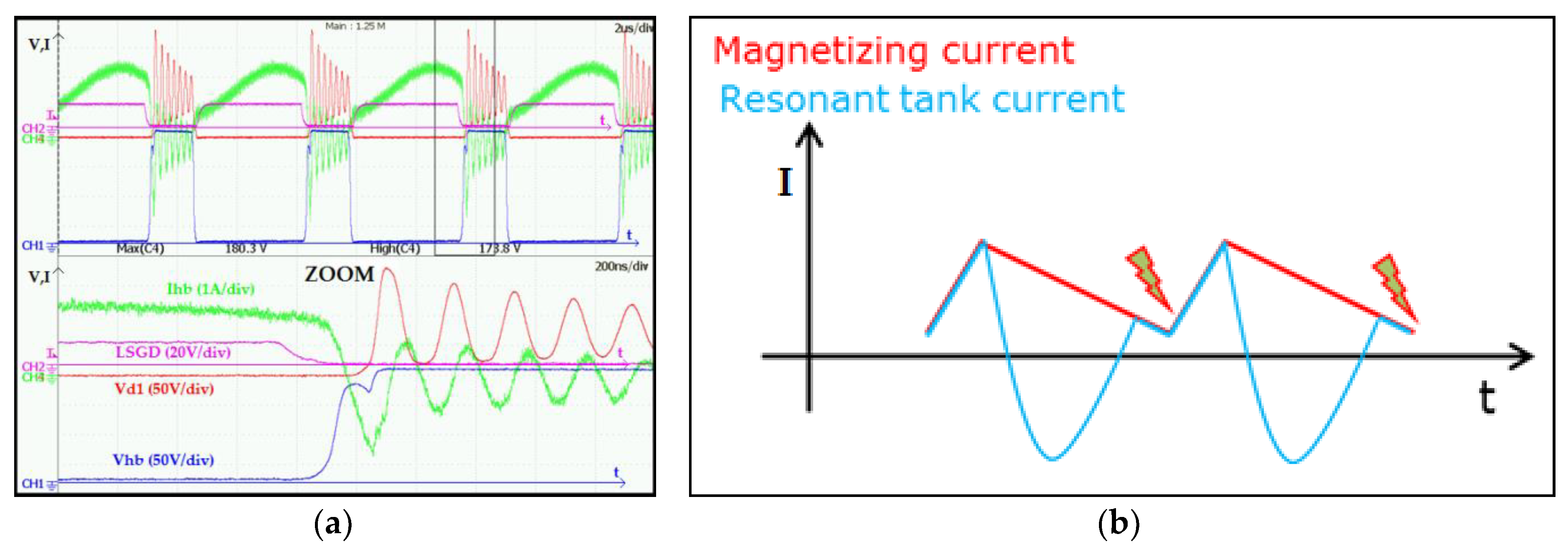
Figure 4b shows that the use of a too-high switching frequency, or high inductance, does not allow the transformer magnetizing current to reverse its polarity when Q2 is switched off. This condition forces the tank current to flow through the body diode of Q2. When Q1 is switched on, a high current will flow through the half-bridge due to the reverse recovery time of the diode, eventually damaging the MOSFETs.
3.3. Proposed Resonant Operation
Taking into account all the considerations previously described, the proposed control method is based on keeping the energy transfer time (Tt) constant (t3 to t5 in Figure 3), and approximately equal to a value around half of the resonant period of circuit formed by Cr and Lr. The regulation of the converter is then achieved by modulating the on time of the high side switch (Q1) (t0 to t2 in Figure 3). This method is illustrated in detail in Section 3.5.
This approach with the proper dimensioning of the topology [9] has the following advantages:
- (a)
- Zero current switching (ZCS) in the secondary side, which avoids losses in the secondary side snubber due to the non-zero current in the secondary leakage inductance.
- (b)
- It allows an easier drive of the synchronous rectifier because it avoids late switch off, i.e., as happened in CCM-operated flyback converters [6].
- (c)
- It avoids double SR (synchronous rectifier) pulses as can happen in active clamp flyback converters [3].
- (d)
- It results in an output current waveform that has a lower RMS (root mean square) value compared to other topologies, such as standard flyback or active clamp flyback converters, by reducing resistive losses (as shown in Figure 3).
3.4. Understanding the Energy Storage
Looking at the energy stored during the charging phase helps to understand why this topology allows a reduction of the size of the transformer compared to a standard or active clamp flyback converter when the same switching frequency is used. While in a standard flyback or ACF (Active Clamp Flyback) all the energy has to be stored in the transformer before releasing it to the secondary side, in the asymmetrical flyback converter, the energy stored is shared between the resonant capacitor and the transformer, resulting in a more relaxed transformer requirement and therefore a smaller size.
Under the condition that the charge time is very small compared to the resonant period (), the increment of stored energy in the resonant capacitor (Cr) and the transformer primary inductance (Llk + Lm) depends on the voltage shared between both of them during the charge phase; this is shown in Figure 2a, considering that the average voltage across the resonant capacitor is proportional to the output voltage and equal to:
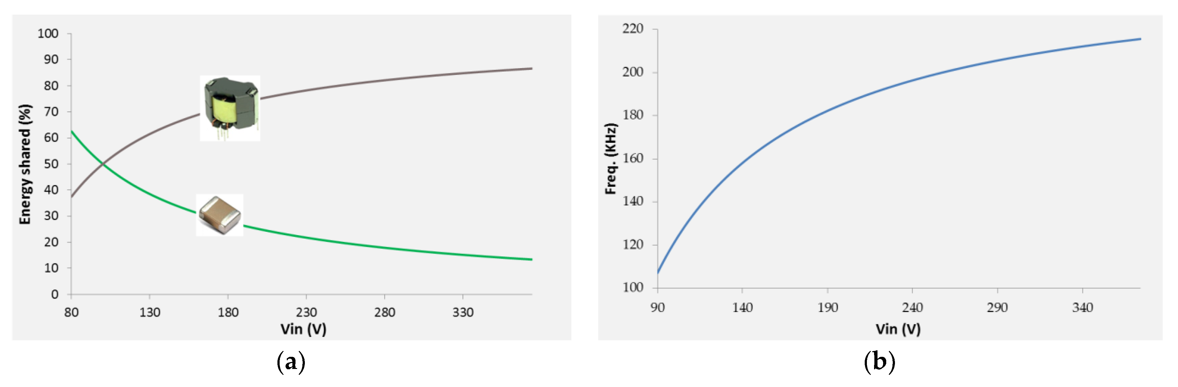
It easy to note that the percentage of energy shared depends on the input voltage as shown in Figure 5a.
It can be observed in Figure 3 that the power taken from the input source, under the condition , can be calculated by the Equation (4):
where Ihb_h and Ihb_l are the Ihb(t) currents at t0 and t2, see Figure 3, and T is the period from t0 to t6.
On the other hand, with the same approximation, the charge (tc) and discharge (td = Tt) times of the transformer can be determined by the voltage applied to the transformer during each phase:
where Ihb_pp = Ihb_h − Ihb_l.
Neglecting dead times, the period T can be extracted by adding tc and td. By replacing T and tc in Equation (4), the following expression for the input power can be derived:
Assuming an ideal system with no losses, where all the energy taken from the input is transferred to the output (Pin = Pout), Iout can be calculated as follows:
Equation (8) shows that for the given control method the output current is independent of the input and output voltages.
From Figure 5 it can be observed that for the higher input voltages the portion of power transferred from the resonant capacitor is lower; this means that the transformer always stores the same amount of energy (same Ihb_h and Ihb_l over the input voltage) but it transfers more power because of the higher switching frequencies. This is different behavior compared to a standard flyback converter or an ACF converter where the transformer is the only element storing the energy. Here, the frequency decreases with lower input voltages and the transformer is forced to store more energy leading to higher core flux and losses.
3.5. Magnetizing Current Displacement
With the proposed control method, where Tt is kept constant and therefore Ihb_pp = Ihb_h − Ihb_l, Equation (8) demonstrates the shift of the transformer T1 magnetizing current due to the output current.
Under the conditions of a constant output voltage (constant duty cycle) and zero output current, the equivalent circuit is a half-bridge driving an LC tank formed by the transformer primary inductance (Lr + Lm) and Cr (no secondary elements involved). The amount of Ihb peak to peak depends only on the applied frequency or Tt. The converter only circulates energy: No energy is transferred to the secondary side.
As the output current increases, the reflected current of the secondary side appears in the primary side, as shown in Figure 3 from t3 to t5. If the output voltage is constant, the reflected current shifts the magnetizing current up by approximately a factor of 2Iout/N, where N is the transformer turns ratio.
The magnetizing current can be used to estimate the average output current or to control it independently of the input and output voltages, i.e., by measuring the middle point of the increasing current ramp during Q1 on time, t0 to t2 in Figure 3.
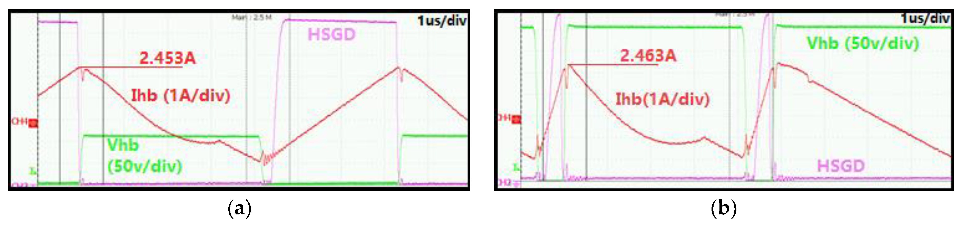
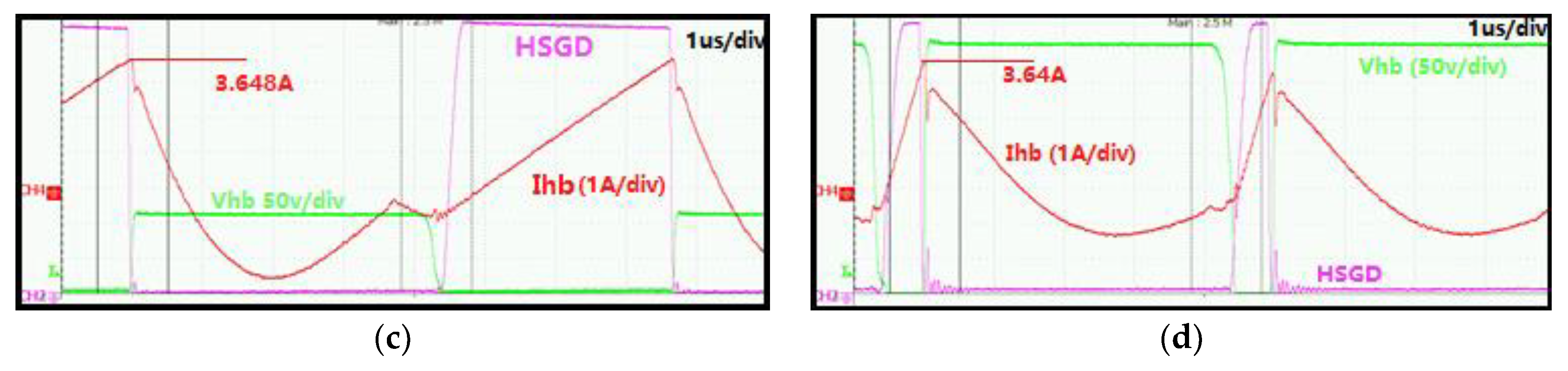
Figure 6 shows actual measurements of the effect of the input voltage and the output current on the magnetizing current. In particular, Figure 6a,b show that the peak current of the tank circuit is independent of the input voltage and has the same peak value because the output load is the same, 0.6 A. Figure 6c,d show the same effect with a load of 3.25 A. The value of Ihb peak current is given by Equation (9).
3.6. Overpower Capability
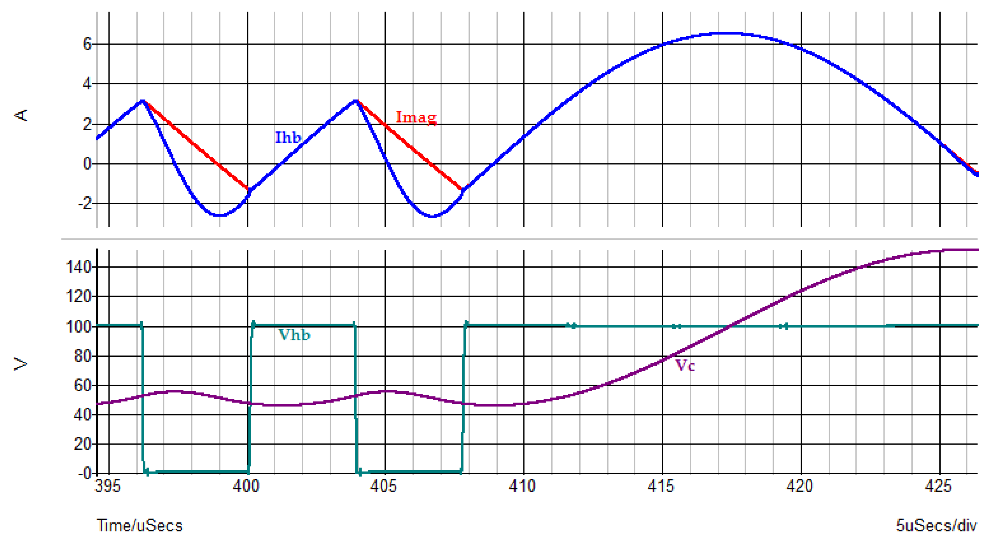
Until this point the description of the behavior of the converter has been based on the assumption of a very small variation of the resonant capacitor voltage. Without the previous approximation , the primary current during the charge time is not linear but sinusoidal with a resonance period given by:
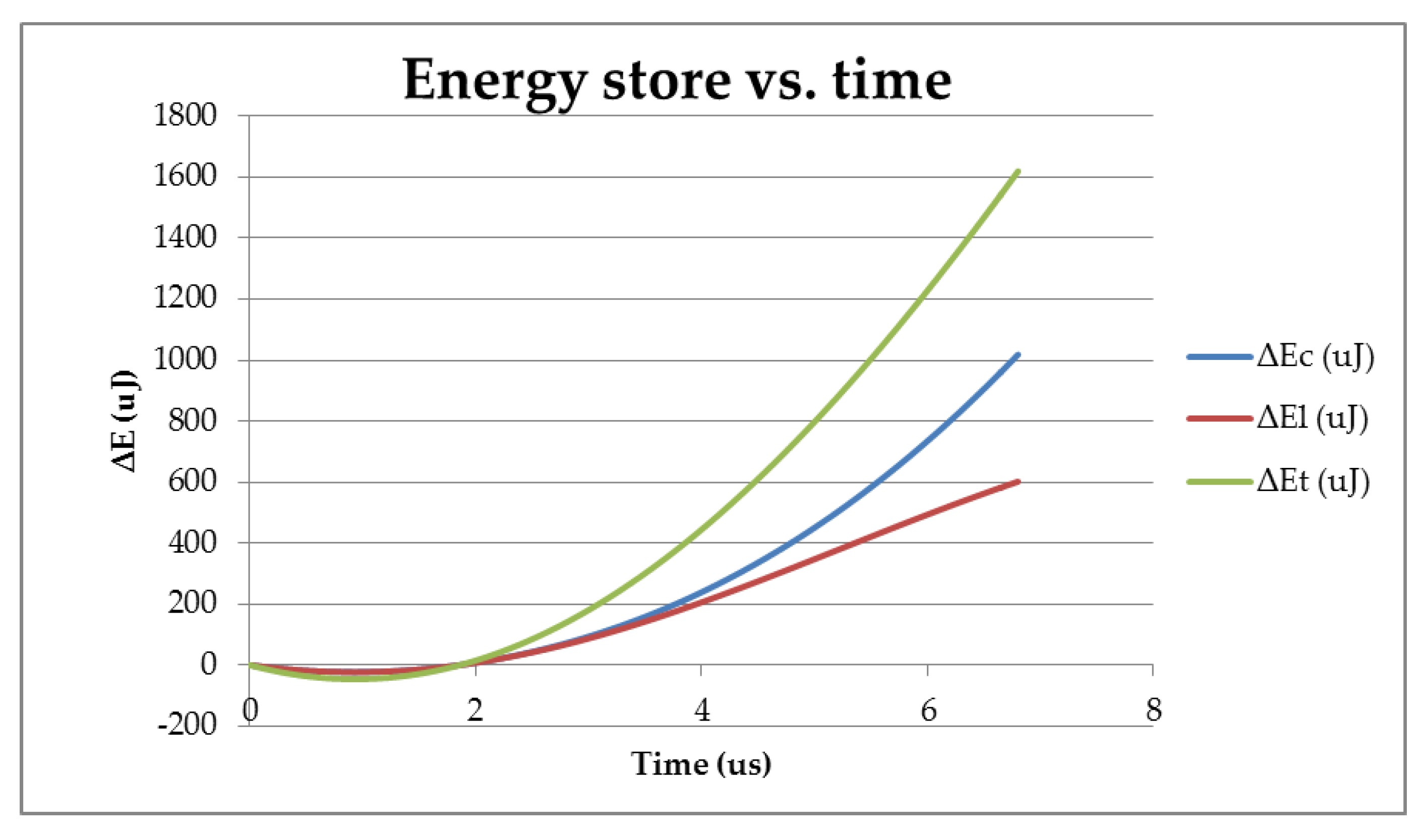
Under heavy load conditions, where longer charge times are required, it can be observed that the percentage of energy accumulated by the capacitor is even larger compared with the approximation previously used of small tc time. Figure 7 shows the magnetizing current and resonant capacitor voltage over time, and Figure 8 shows the stored energy of each element over time.
Such behavior can be used to provide a considerable amount of overpower, often required in adaptors without the risk of saturating the transformer as can happen in standard flyback or active clamp flyback (ACF) converters.
4. Experimental Results
To demonstrate the high efficiency and power density that this topology can achieve, a 65 W prototype converter was built. The converter specifications are shown in Table 1.
The dimensioning of the converter was determined according to [11] and the feedback network was determined considering [13]. A synchronous rectifier was used on the secondary side in order to further boost the efficiency. The MOSFETs used in this experiment are shown in Table 2. To maximize the efficiency, the primary side switches were selected with a low Rds(on) and a low output capacitance Co(tr) to allow a ZVS with a minimum circulating current. Since the half-bridge transistor’s body diode clamps the Vhb, there was no need for a very high voltage rating of these elements as in a standard flyback converter or ACF converter. For the control, a programmable digital controller from Infineon was used.
The transformer was implemented using an RM8 core. The specifications are shown in Table 3:
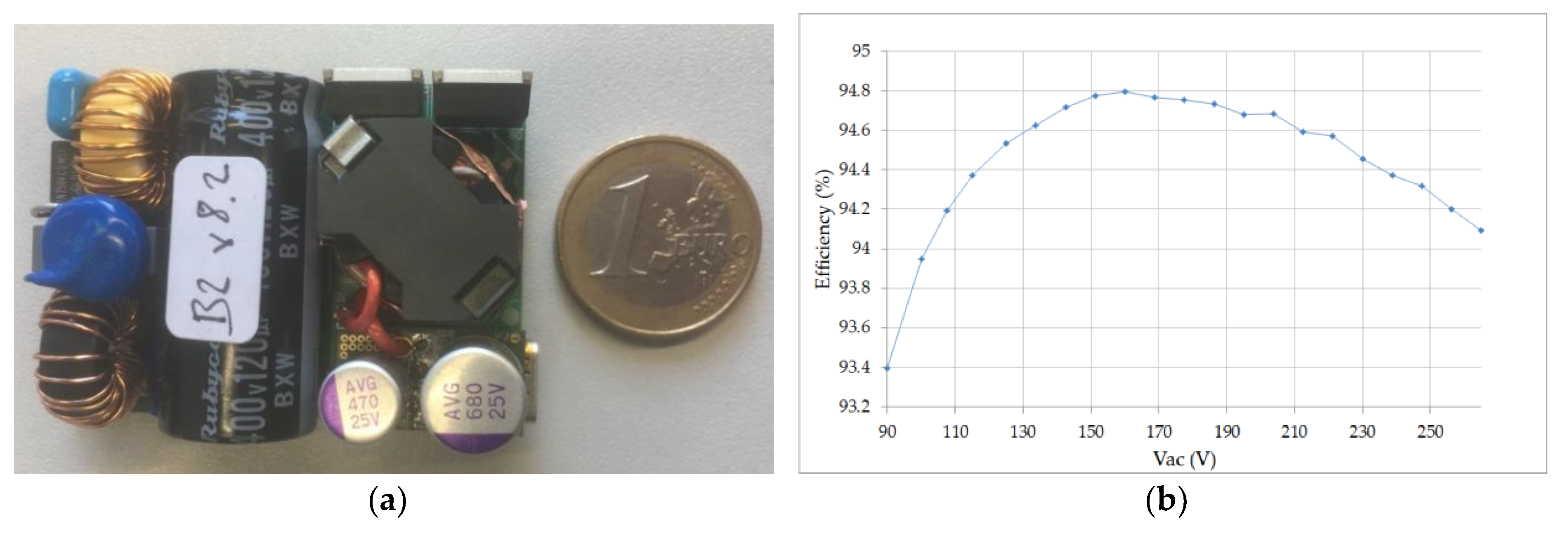
The dimensions of the final converter (see Figure 9a) were 51.5 × 38 × 19 mm, achieving a power density of 29 W/inch3. The prototype achieved a minimum efficiency of 93.4 at a 90 Vac input and a 65 W load measured at the board connectors.
The frequency of operation ranged from approximately 100 KHz at 90 Vac to 200 KHz at 264 Vac.
The equipment used for measurements is listed in Table 4:
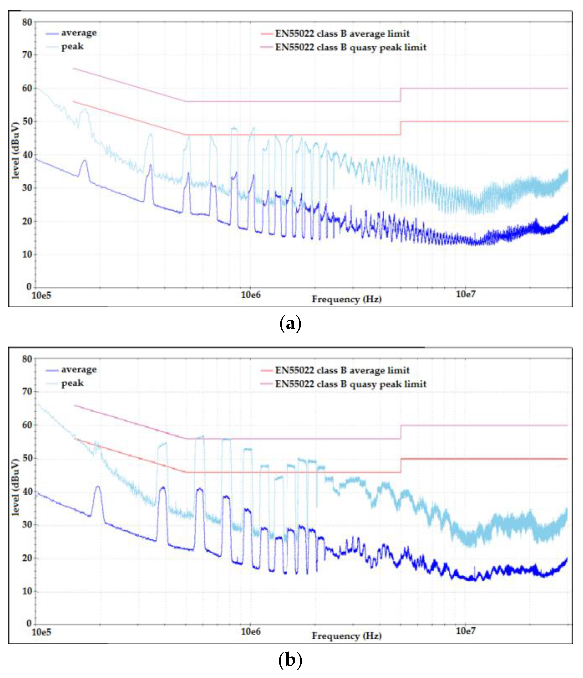
Figure 10 shows the EMI results, demonstrating the benefits of this topology and the used control method.
5. Discussion
The outstanding efficiency and EMI performance of the asymmetrical duty cycle flyback converter were proven. The proposed converter and its control method, including ZVS and ZCS over load and line, enable the future study of the benefits of using faster switching devices and higher switching frequencies. This could result in the reduction of the transformer size, and the extension of the input voltage range to further reduce the bulk capacitor or to increase the leakage inductance to achieve EMI requirements at higher switching frequencies.
When used in a DC-to-DC stage and with the proper design, it can achieve efficiency levels close to an LLC converter but with the benefit of the wider voltage range, meaning that in some cases the replacement may be possible and beneficial.
6. Conclusions
The proposed asymmetric flyback with the presented control method is a promising topology for highly efficient and very compact adaptors. These features were achieved due to its forward energy transfer capability, compared to standard flyback or ACF [14], where the transformer has to store all the energy. The proposed control method and topology recycle the energy of the most critical parasitic elements and ensure ZVS and ZCS over load and line. Even with the use of slow devices (with respect to GaN), the efficiency is high and the EMI, due to slow voltage slew rates, easily fulfills commercial requirements.
The performance was demonstrated with a 65W prototype that achieves a minimum efficiency of 93.4% and a peak of 94.8% at full load over the range of Vac input voltage, satisfying the EN55022 class B requirements.
Author Contributions
Conceptualization, A.M.G. and M.S.; Supervision, D.P.M. and N.R.; Validation, A.M.G. and M.S.; Writing—original draft, A.M.G.; Writing—review, discussion and editing, A.M.G., M.S., D.P.M. and N.R.
Funding
This research is financed by Infineon Tecnologias AG.
Conflicts of Interest
The authors declare no conflict of interest.
References
- Panepinto, P.A. Making power adapters smarter and greener. In Proceedings of the 2009 IEEE International Symposium on Sustainable Systems and Technology, Phoenix, AZ, USA, 18–20 May 2009; pp. 1–5. [Google Scholar] [CrossRef]
- Steigerwald, R.L.; de Doncker, R.W.; Kheraluwala, M.H. A comparison of high power DC-to-DC soft-switched converter topologies. In Proceedings of the 1994 IEEE Industry Applications Society Annual Meeting, Denver, CO, USA, 2–6 October 1994; Volume 2, pp. 1090–1096. [Google Scholar] [CrossRef]
- Alou, P.; Garcia, O.; Cobos, J.A.; Uceda, J.; Rascon, M. Flyback with active clamp: A suitable topology for low power and very wide input voltage range applications. In Proceedings of the APEC Seventeenth Annual IEEE Applied Power Electronics Conference and Exposition (Cat. No. 02CH37335), Dallas, TX, USA, 10–14 March 2002; Volume 1, pp. 242–248. [Google Scholar] [CrossRef]
- Watson, R.; Lee, F.C.; Hua, G.C. Utilization of an active-clamp circuit to achieve soft switching in flyback converters. IEEE Trans. Power Electron. 1996, 11, 162–169. [Google Scholar] [CrossRef]
- Deboy, G.; Kasper, M.J.; Medina-Garcia, A.; Schlenk, A. A New Era in Power Electronics with Gallium Nitride. ETG J. Infineon Article 2018, 2, 6. [Google Scholar]
- Papanikolaou, N.P.; Tatakis, E.C. Active voltage clamp in flyback converters operating in CCM mode under wide load variation. IEEE Trans. Ind. Electron. 2004, 51, 632–640. [Google Scholar] [CrossRef]
- Pala, V.; Barkley, A.; Hull, B.; Wang, G.; Ryu, S.H.; Van Brunt, E.; Lichtenwalner, D.; Richmond, J.; Jonas, C.; Capell, C.; et al. 900V silicon carbide MOSFETs for breakthrough power supply design. In Proceedings of the 2015 IEEE Energy Conversion Congress and Exposition (ECCE), Montreal, QC, Canada, 20–24 September 2015; pp. 4145–4150. [Google Scholar] [CrossRef]
- Garcia-Rodriguez, L.; Williams, E.; Balda, J.C.; Gonzalez-Llorente, J.; Lindstrom, E.; Oliva, A. Dual-stage microinverter design with a GaN-based interleaved flyback converter stage. In Proceedings of the 2013 IEEE Energy Conversion Congress and Exposition, Denver, CO, USA, 15–19 September 2013; pp. 4496–4502. [Google Scholar] [CrossRef]
- Lim, S.H. Asymmetrical Duty Cycle Flyback Converter. U.S. Patent US5959850A, 28 September 1999. [Google Scholar]
- Li, H.; Zhou, W.; Zhou, S.; Yi, X. Analysis and design of high frequency asymmetrical half bridge flyback converter. In Proceedings of the 2008 International Conference on Electrical Machines and Systems, Wuhan, China, 17–20 October 2008; pp. 1902–1904. [Google Scholar]
- Garcia, A.M.; Kasper, M.J.; Schlenk, M.; Deboy, G. Asymmetrical flyback converter in high density SMPS. In Proceedings of the PCIM 2018, Nuremberg, Germany, 5–7 June 2018. [Google Scholar]
- Huber, L.; Jovanović, M.M. Analysis, Design and Performance Evaluation of Asymmetrical Half-Bridge Flyback Converter for Universial-LineVoltage-Range Applications. In Proceedings of the Applied Power Electronics Conference and Exposition (APEC 2017), Tampa, FL, USA, 26–30 March 2017. [Google Scholar]
- Chen, T.M.; Chen, C.L. Small-Signal Modeling of Asymmetrical Half Bridge Flyback Converter. In Proceedings of the CES/IEEE 5th International Power Electronics and Motion Control Conference National, Shanghai, China, 14–16 August 2006. [Google Scholar]
- Xue, L.; Zhang, J. Active clamp flyback using GaN power IC for power adapter applications. In Proceedings of the 2017 IEEE Applied Power Electronics Conference and Exposition (APEC), Tampa, FL, USA, 26–30 March 2017; pp. 2441–2448. [Google Scholar]
Figure 1.
Simplified adaptor schematic of an asymmetric pulse width modulation (PWM) half-bridge (HB) flyback.
Figure 1.
Simplified adaptor schematic of an asymmetric pulse width modulation (PWM) half-bridge (HB) flyback.

Figure 2.
Asymmetric flyback converter operation phases.

Figure 3.
Resonant asymmetric flyback converter waveforms, Ihb: tank current, Vhb: half bridge middle point voltage, Isec: secondary transformer current.
Figure 3.
Resonant asymmetric flyback converter waveforms, Ihb: tank current, Vhb: half bridge middle point voltage, Isec: secondary transformer current.

Figure 4.
Undesired conditions for ZVS operation: (a) ZVS is achieved with Lr, large oscillations are observed in D1 voltage due to secondary leakage inductance (b) tank current polarity does not allow ZVS operation and leads to body diode cross-conduction when Q1 is switched on.
Figure 4.
Undesired conditions for ZVS operation: (a) ZVS is achieved with Lr, large oscillations are observed in D1 voltage due to secondary leakage inductance (b) tank current polarity does not allow ZVS operation and leads to body diode cross-conduction when Q1 is switched on.

Figure 5.
(a) Percentage of energy stored during the charge phase of the converter over Vin, Vcr = 50 V; (b) switching frequency of the resonant converter over Vin using the proposed control method.
Figure 5.
(a) Percentage of energy stored during the charge phase of the converter over Vin, Vcr = 50 V; (b) switching frequency of the resonant converter over Vin using the proposed control method.

Figure 6.
Converter waveforms under different input voltages and load conditions, in this case the turns ratio N is 2.4: (a) Vin: 110 Vdc, Iload: 0.6 A; (b) Vin: 360 Vdc, Iload: 0.6 A; (c) Vin: 110 Vdc, Iload: 3.25A; (d) Vin: 360 Vdc, Iload: 3.25 A.
Figure 6.
Converter waveforms under different input voltages and load conditions, in this case the turns ratio N is 2.4: (a) Vin: 110 Vdc, Iload: 0.6 A; (b) Vin: 360 Vdc, Iload: 0.6 A; (c) Vin: 110 Vdc, Iload: 3.25A; (d) Vin: 360 Vdc, Iload: 3.25 A.


Figure 7.
Primary waveforms over time with long charge time.

Figure 8.
Energy stored in the transformer magnetizing inductance and resonant capacitor over time. ΔEc: increment of energy in the resonant capacitor, ΔEl: increment of energy in the primary inductance, ΔEt: total increment of energy in the resonant tank.
Figure 8.
Energy stored in the transformer magnetizing inductance and resonant capacitor over time. ΔEc: increment of energy in the resonant capacitor, ΔEl: increment of energy in the primary inductance, ΔEt: total increment of energy in the resonant tank.

Figure 9.
(a) Asymmetric flyback converter prototype; (b) full load efficiency versus input voltage range.
Figure 9.
(a) Asymmetric flyback converter prototype; (b) full load efficiency versus input voltage range.

Figure 10.
EMI results for average, dark blue and peak, light blue values. Upper limit: quasi peak, lower limit: average. (a) Result at 115 Vac, full load and (b) result at 230 Vac, full load.
Figure 10.
EMI results for average, dark blue and peak, light blue values. Upper limit: quasi peak, lower limit: average. (a) Result at 115 Vac, full load and (b) result at 230 Vac, full load.


Table 1.
Converter target specifications.
| Parameter | Value |
|---|---|
| Max output current | 3.25 A |
| Output voltage | 20 V |
| Input voltage | 90–264 Vac |
| Power density | >20 w/inch3 |
| Efficiency full load | >93% |
| EMC | EN55022 class B |
Table 2.
MOSFETs characteristics.
| Parameter | HB Mosfets | SR Mosfet |
|---|---|---|
| Manufacturer | Infineon | Infineon |
| Reference | IPP50R140CP | BSC093N15NS5 |
| Rds(on) | 140 mOhm | 9.3 mOhm |
| Vds max | 500 V | 150 V |
| Co(tr) | 230 pF | 604 pF |
| Qgs | 48 nC | 14 nC |
Table 3.
Transformer specifications.
| Parameter | HB Mosfets |
|---|---|
| Core type | RM8 |
| Core material | 3C95 |
| Lm | 52uH |
| Llk | 1.7uH |
| Np | 18 turns (Litz 40 × 0.1 mm) |
| Ns | 7 turns (TIW Litz 70 × 0.1 mm) |
| Winding interleaving | P-S-P |
Table 4.
List of equipment used for measurements.
| Parameter | HB Mosfets |
|---|---|
| AC source | Chroma 61505 |
| Programmable load | Chroma 63202 |
| Power analyzer | Yokogawa WT500 |
| Spectrum analyzer | Rohde&Schwarz HMS-X |
| Oscilloscope | Yokogawa DLM6054 |
© 2018 by the authors. Licensee MDPI, Basel, Switzerland. This article is an open access article distributed under the terms and conditions of the Creative Commons Attribution (CC BY) license (http://creativecommons.org/licenses/by/4.0/).
Share and Cite
MDPI and ACS Style
Medina-Garcia, A.; Schlenk, M.; Morales, D.P.; Rodriguez, N. Resonant Hybrid Flyback, a New Topology for High Density Power Adaptors. Electronics 2018, 7, 363. https://doi.org/10.3390/electronics7120363
AMA Style
Medina-Garcia A, Schlenk M, Morales DP, Rodriguez N. Resonant Hybrid Flyback, a New Topology for High Density Power Adaptors. Electronics. 2018; 7(12):363. https://doi.org/10.3390/electronics7120363
Chicago/Turabian StyleMedina-Garcia, Alfredo, Manfred Schlenk, Diego P. Morales, and Noel Rodriguez. 2018. "Resonant Hybrid Flyback, a New Topology for High Density Power Adaptors" Electronics 7, no. 12: 363. https://doi.org/10.3390/electronics7120363
Note that from the first issue of 2016, this journal uses article numbers instead of page numbers. See further details here.