
Integration of Photovoltaic-Based Transformerless High Step-Up Dual-Output–Dual-Input Converter with Low Power Losses for Energy Storage Applications

 ,
,  , and
, and
Abstract
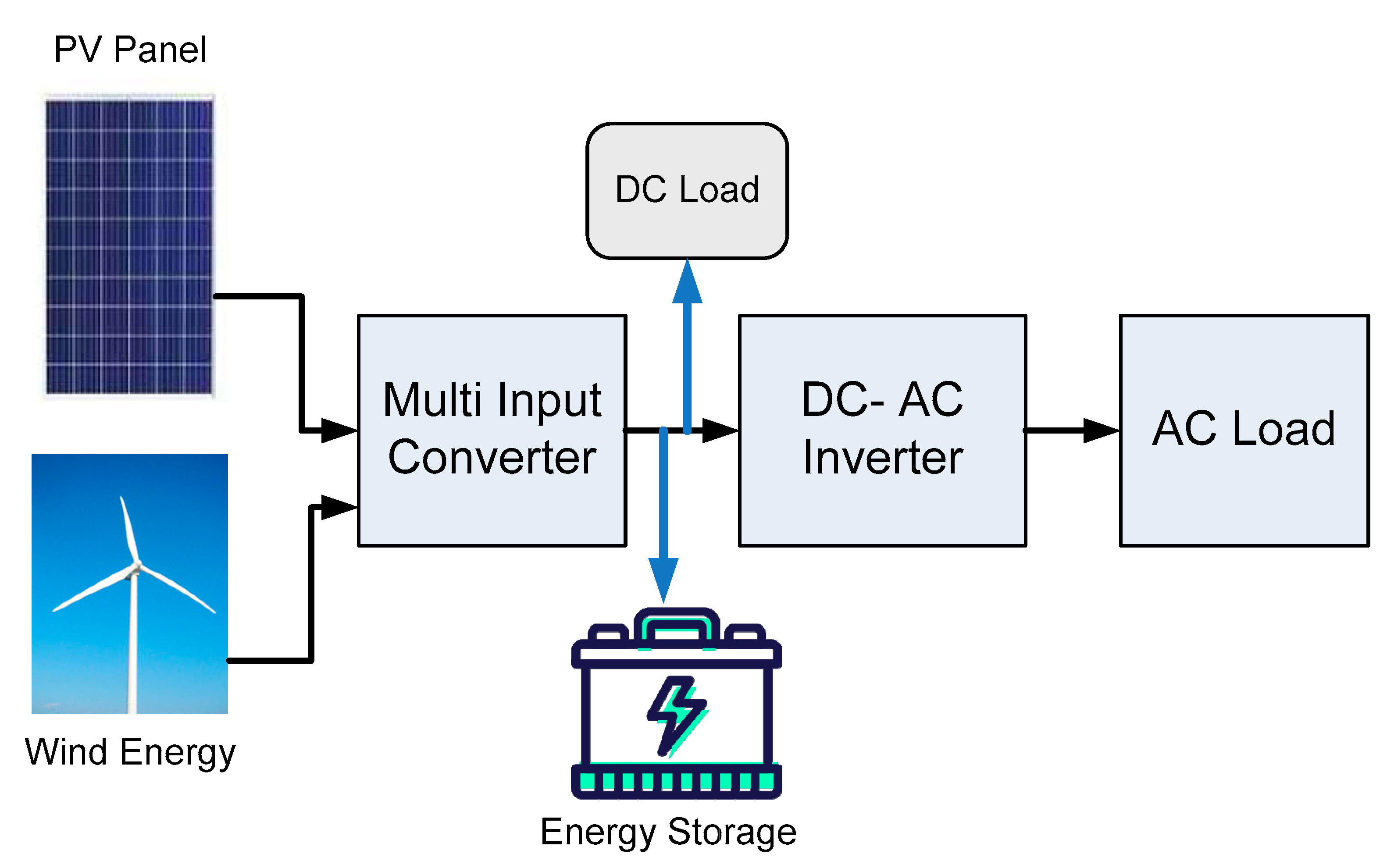
:1. Introduction
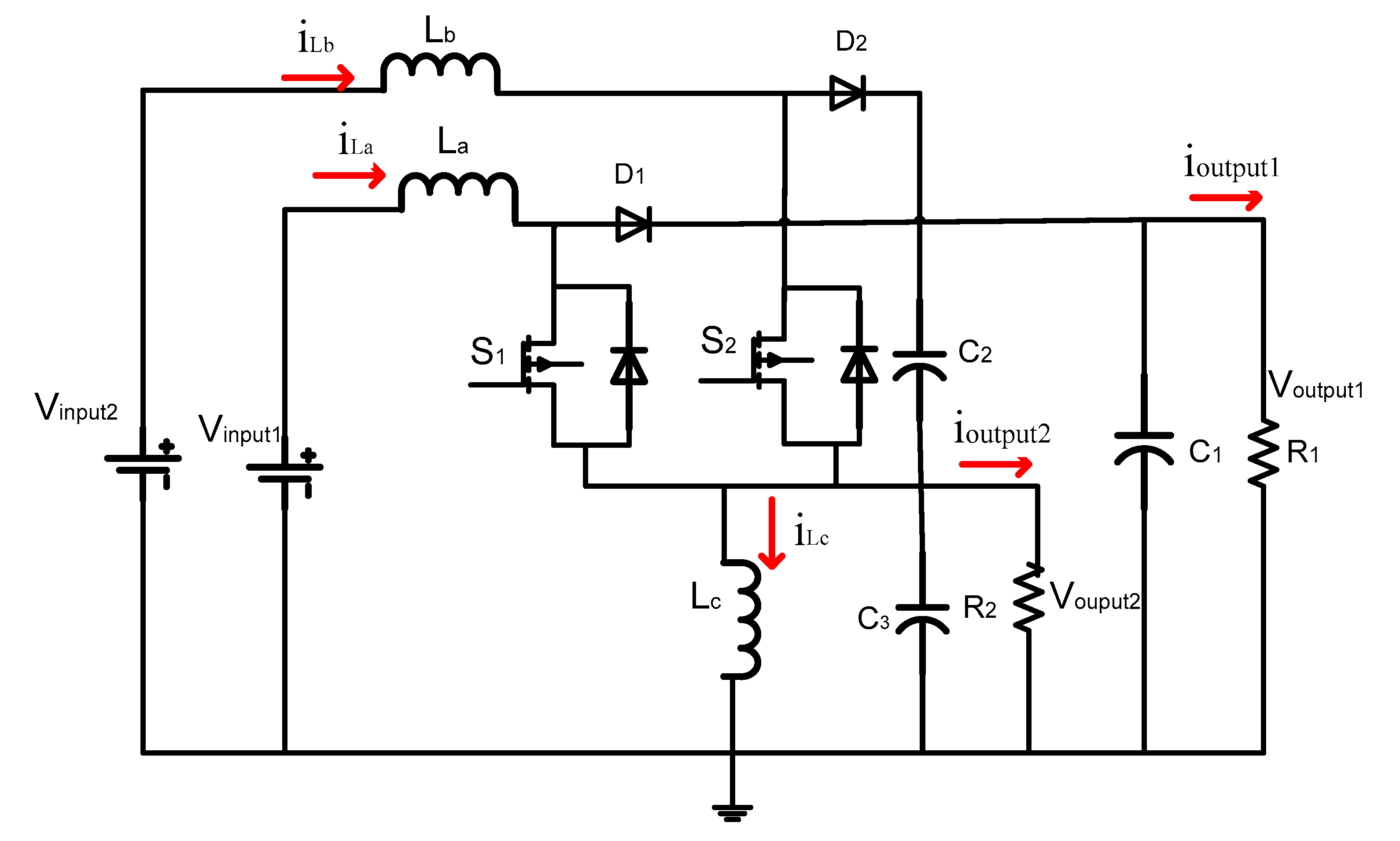
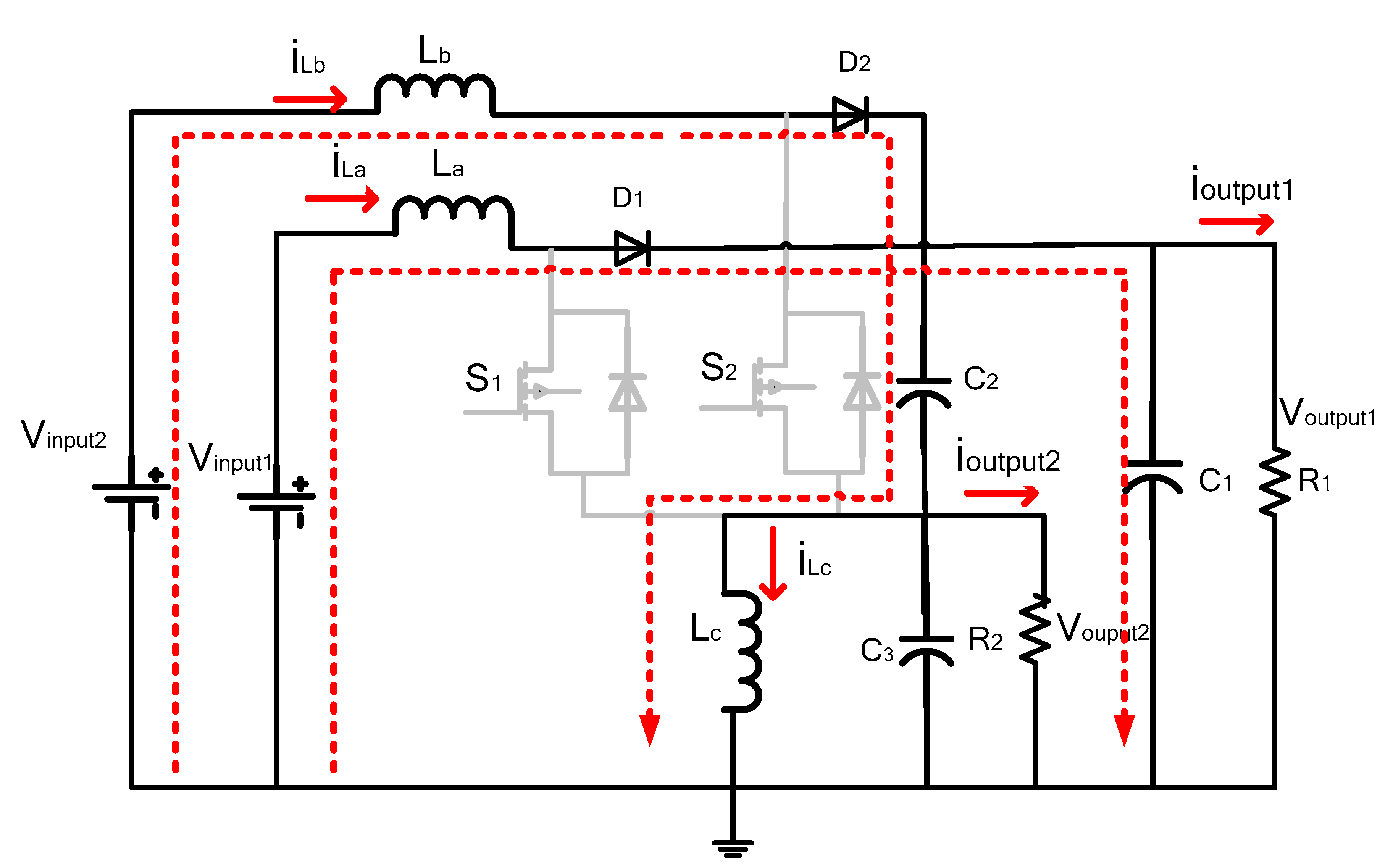
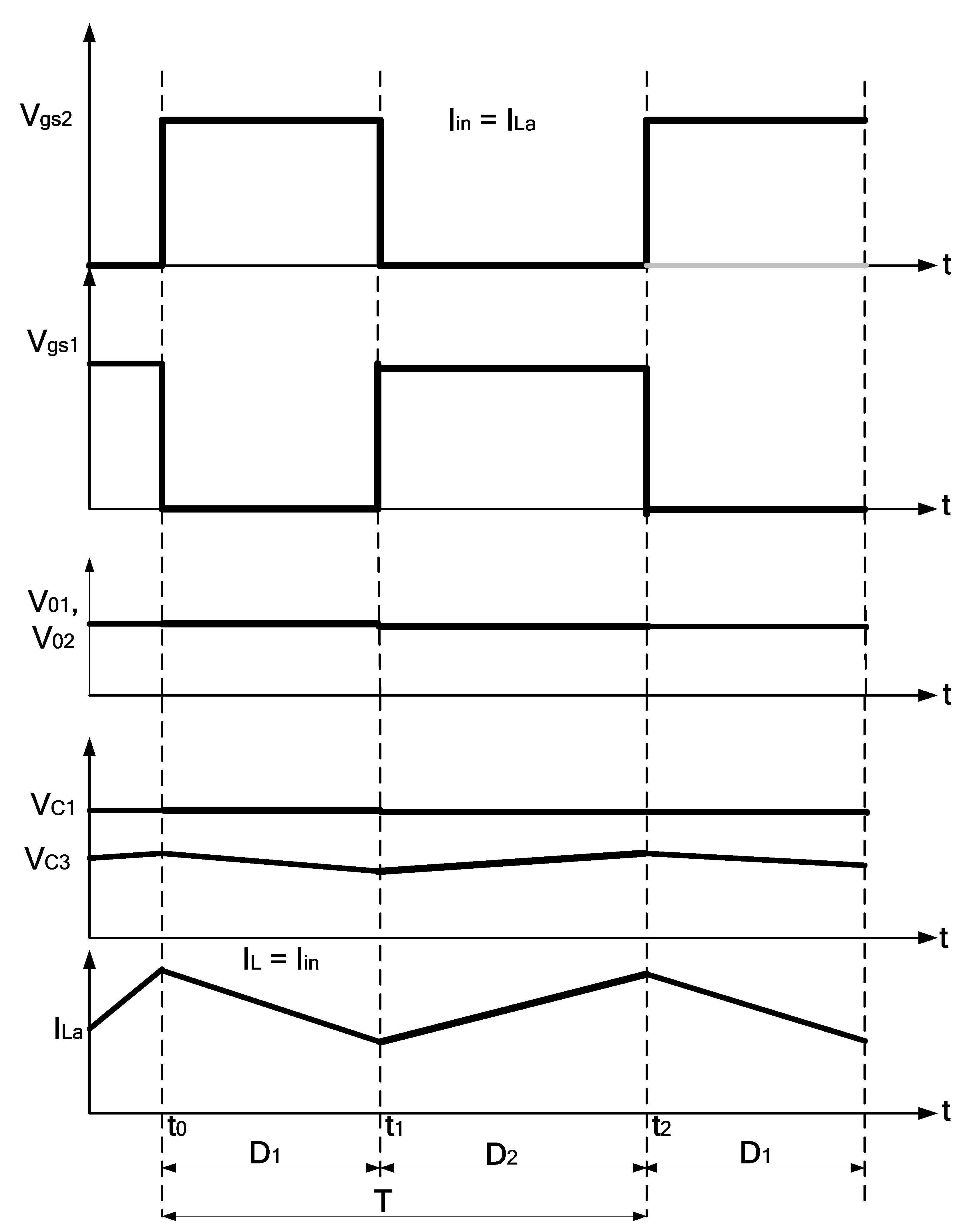
2. Operation of the Proposed Converter
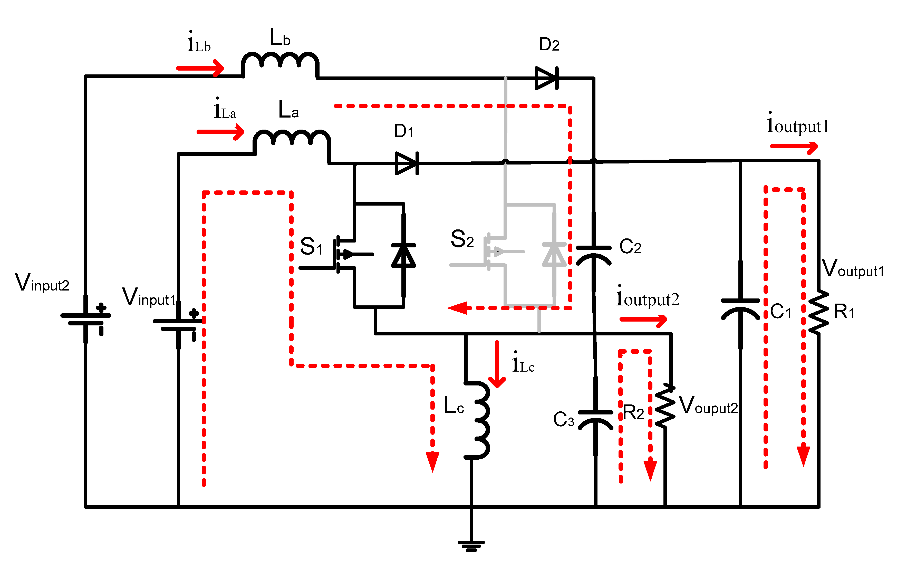
2.1. Mode 1 Operation
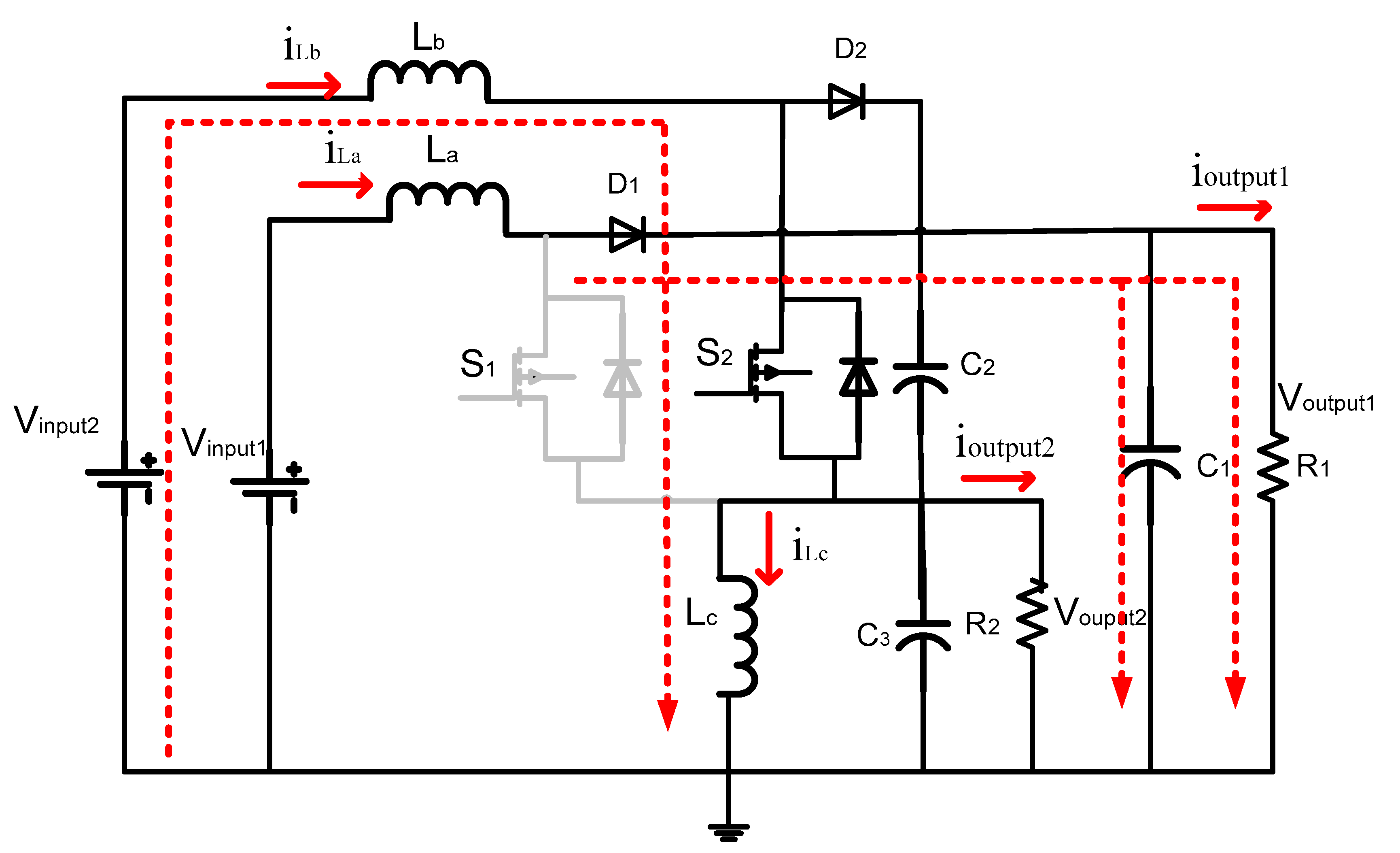
2.2. Mode 2 Operation
2.3. Mode 3 Operation
3. The Proposed MIMO Converter’s Design Process
3.1. Voltage Gain
3.2. Power Consumed by Each Source
3.3. Inductor Selection
3.4. Capacitor Selection
3.5. Stability Analysis
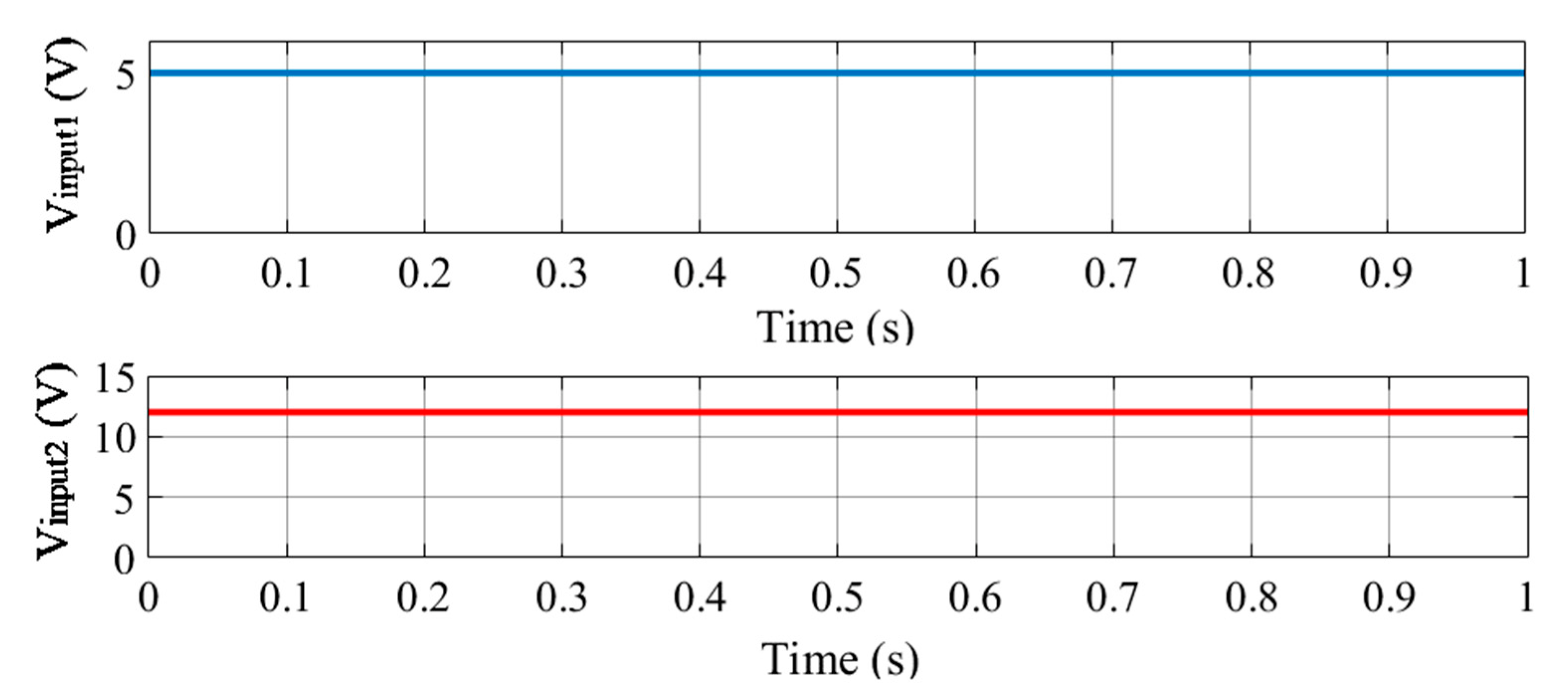
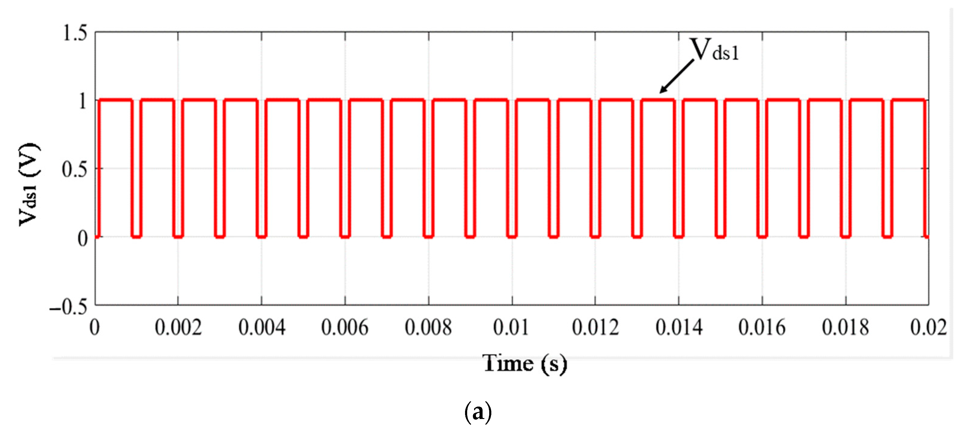
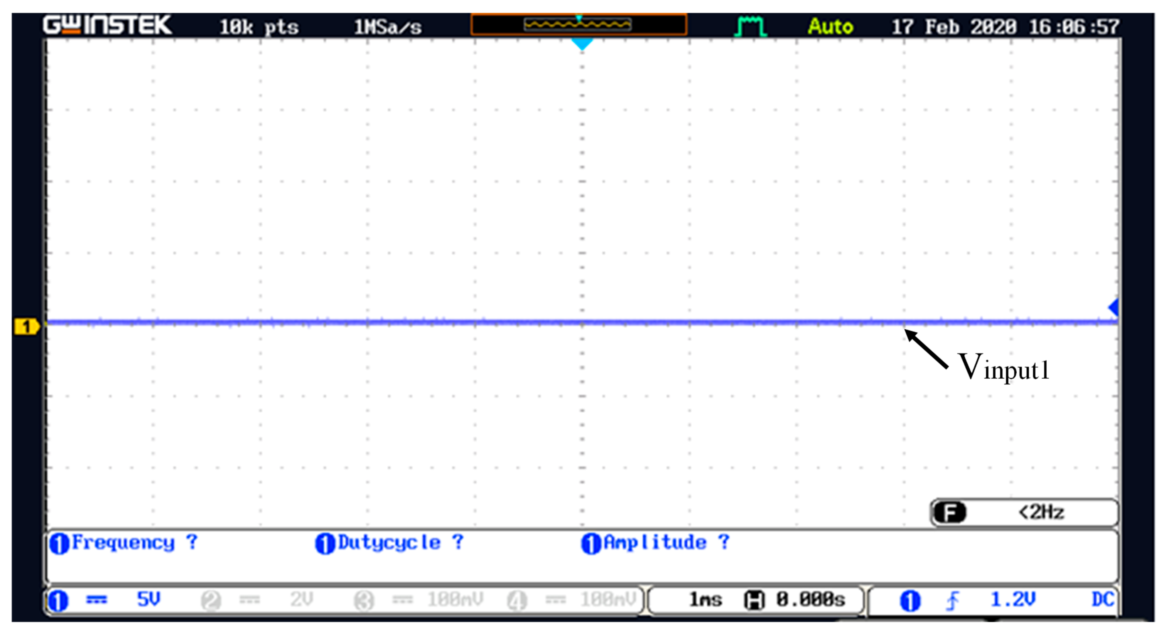
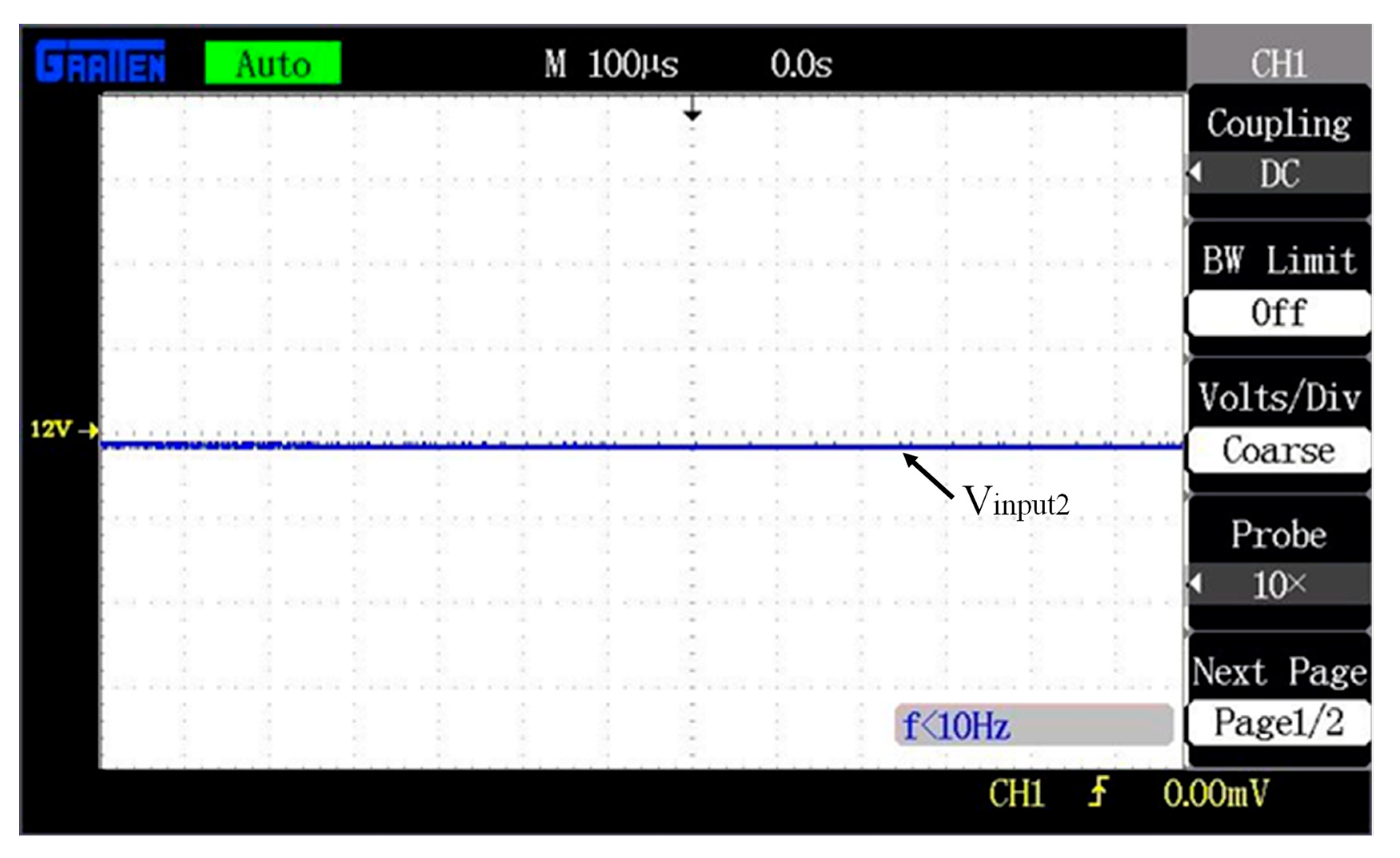
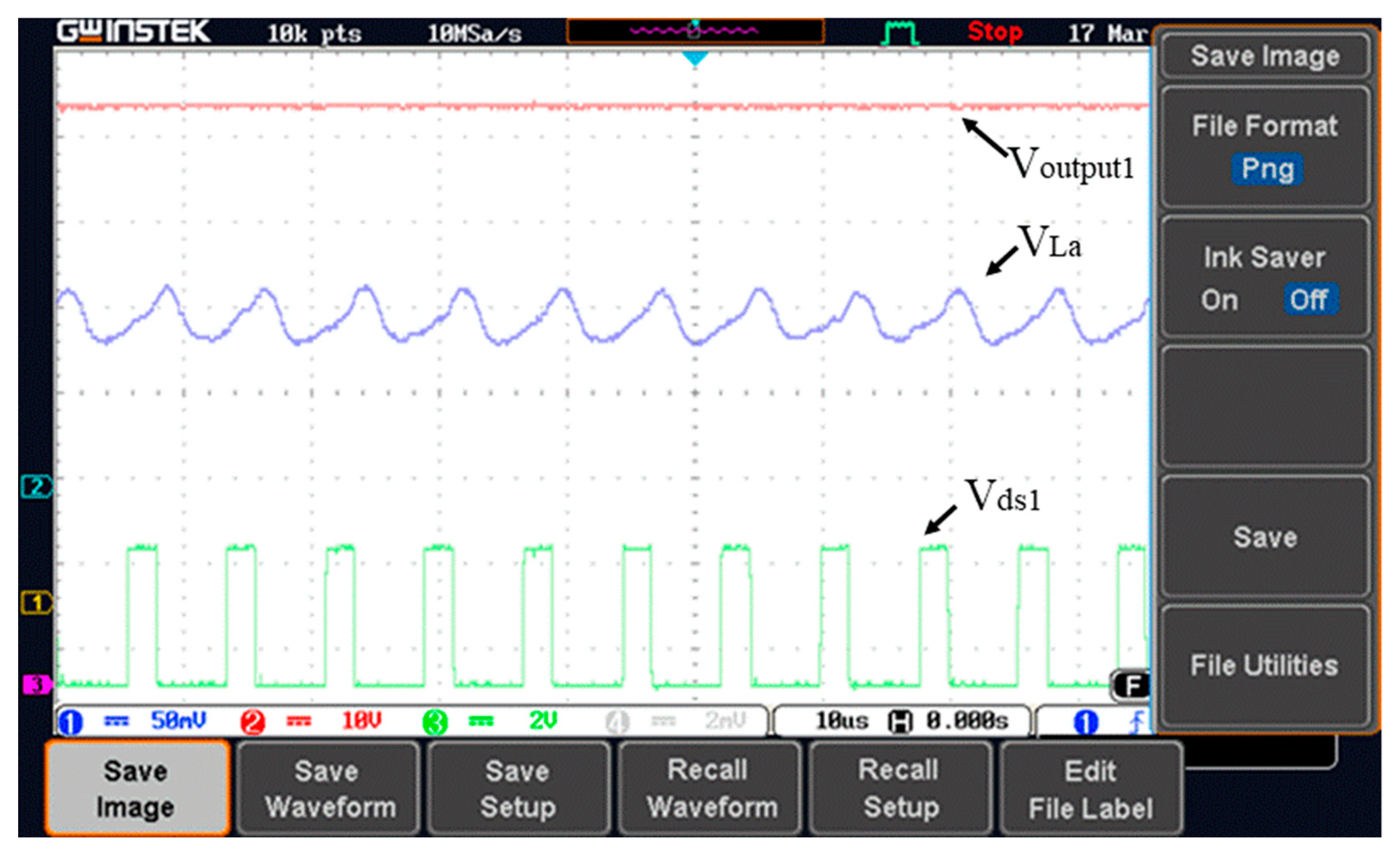
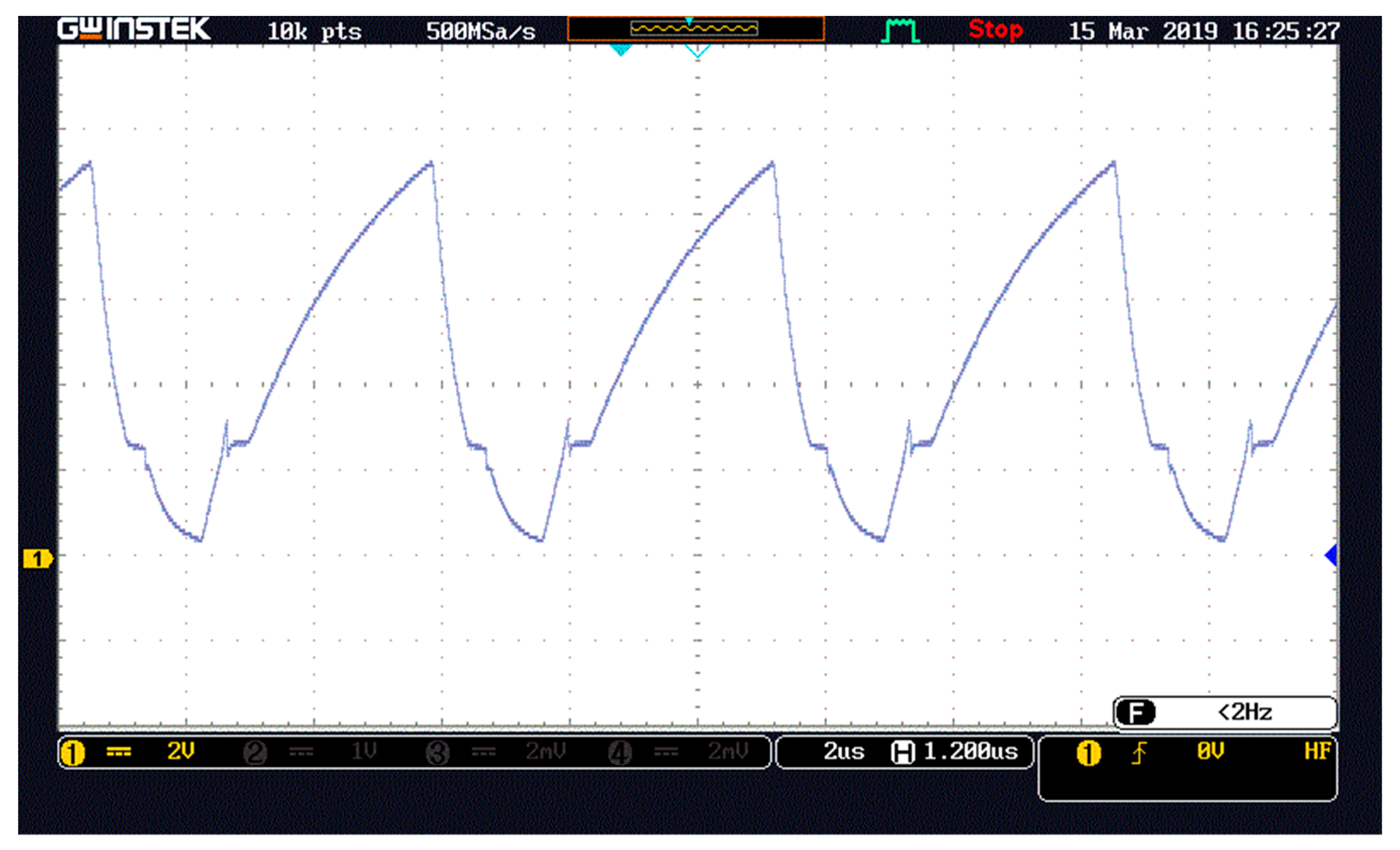
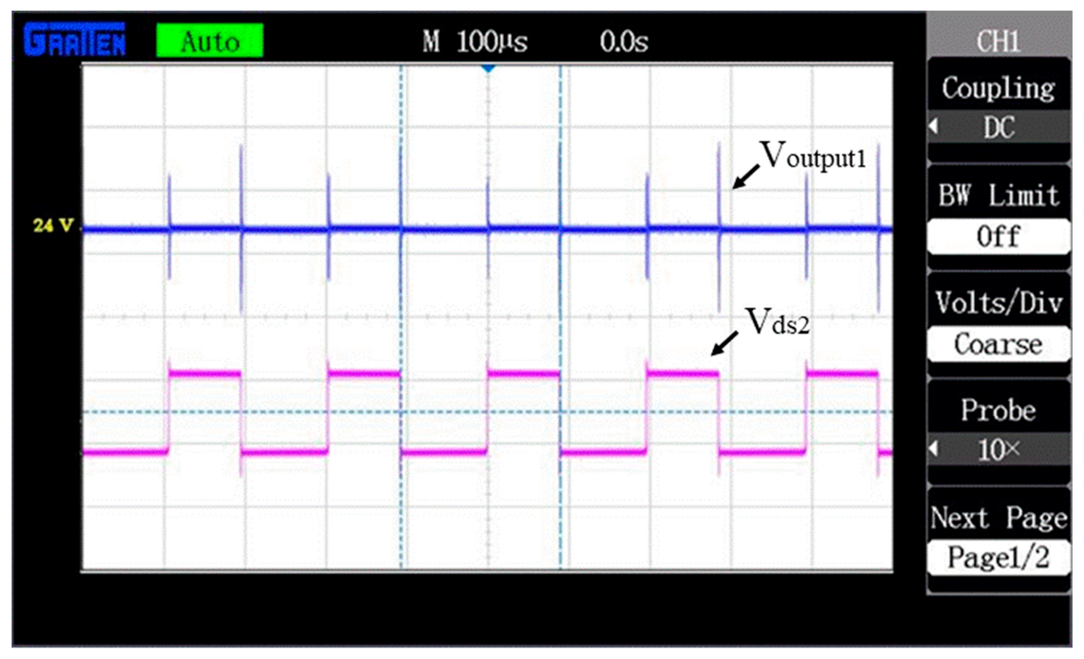
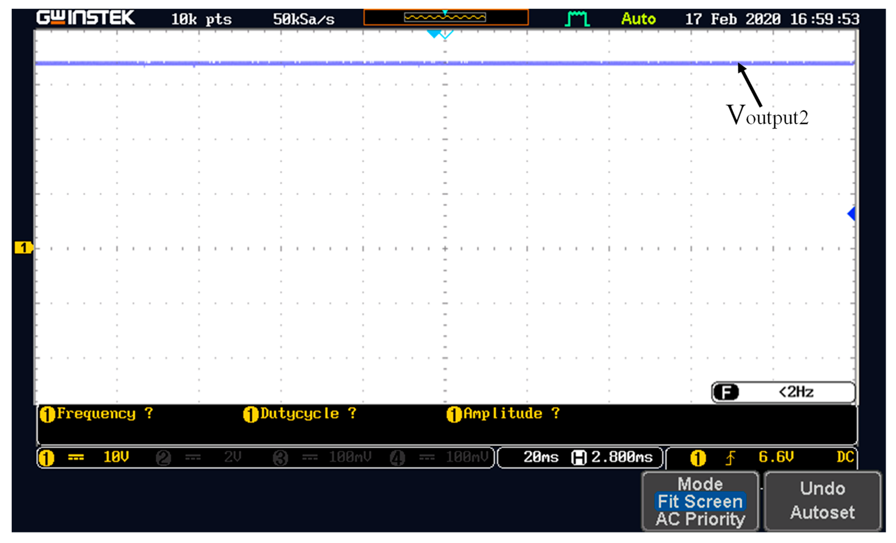
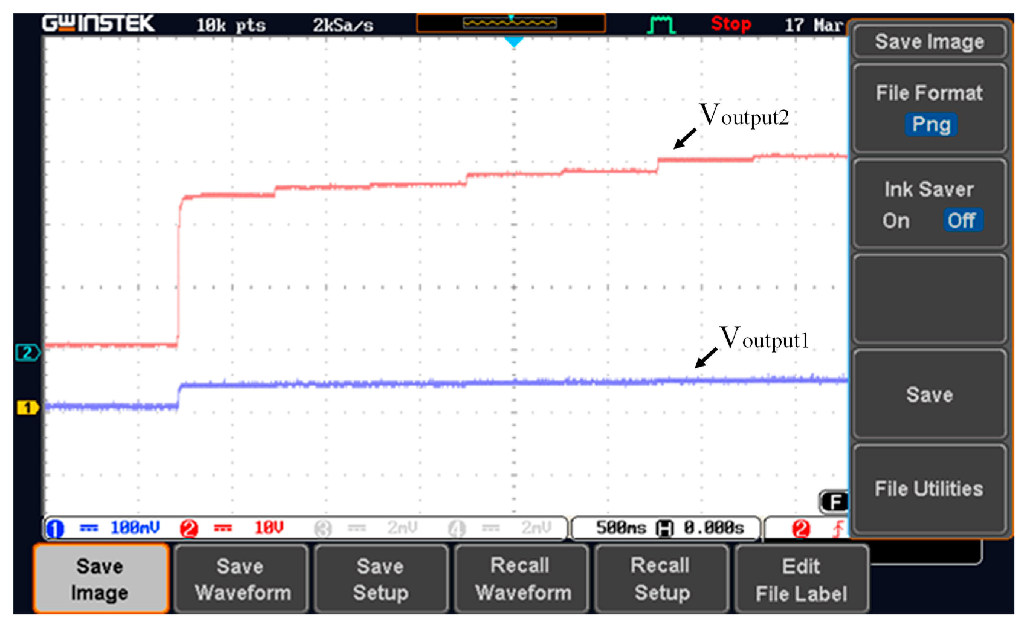
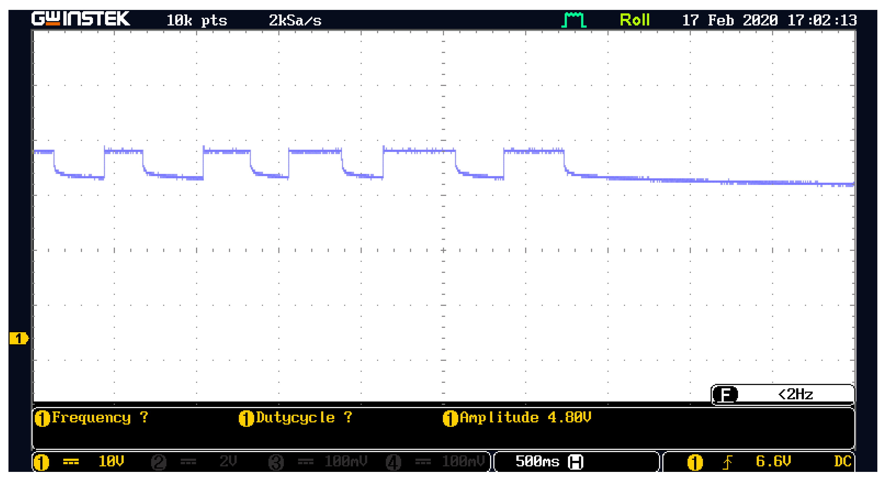
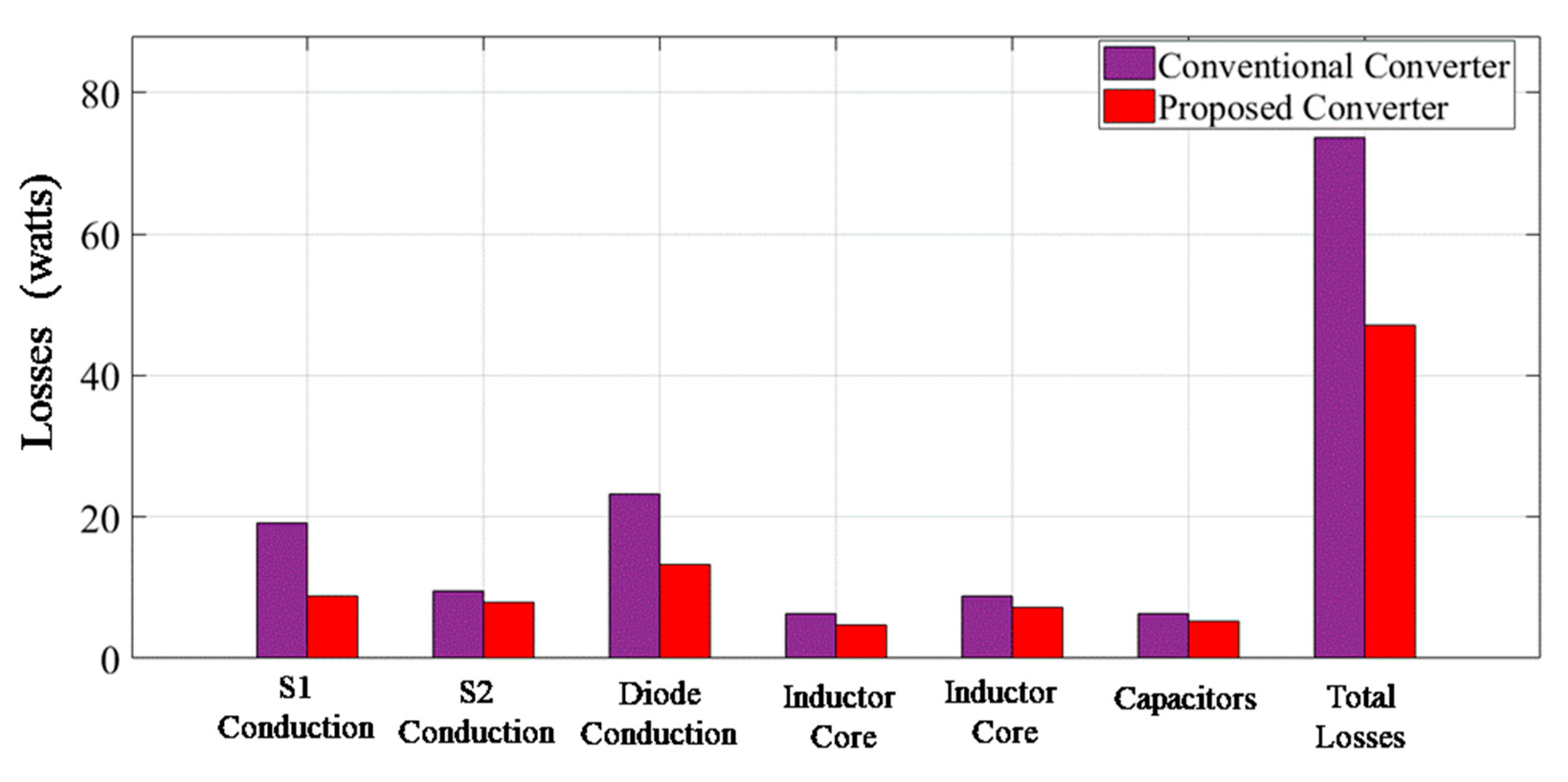
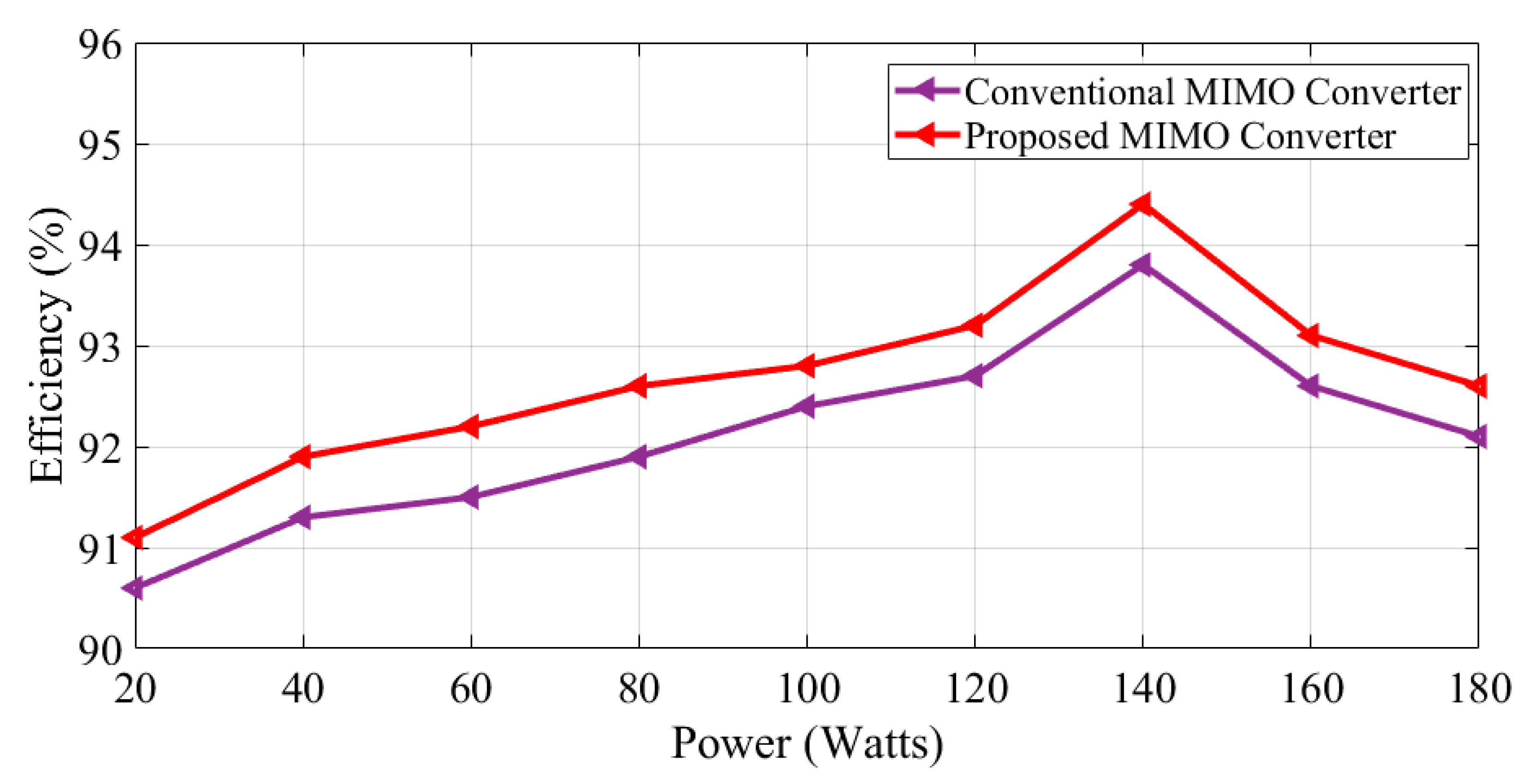
4. Results and Discussion
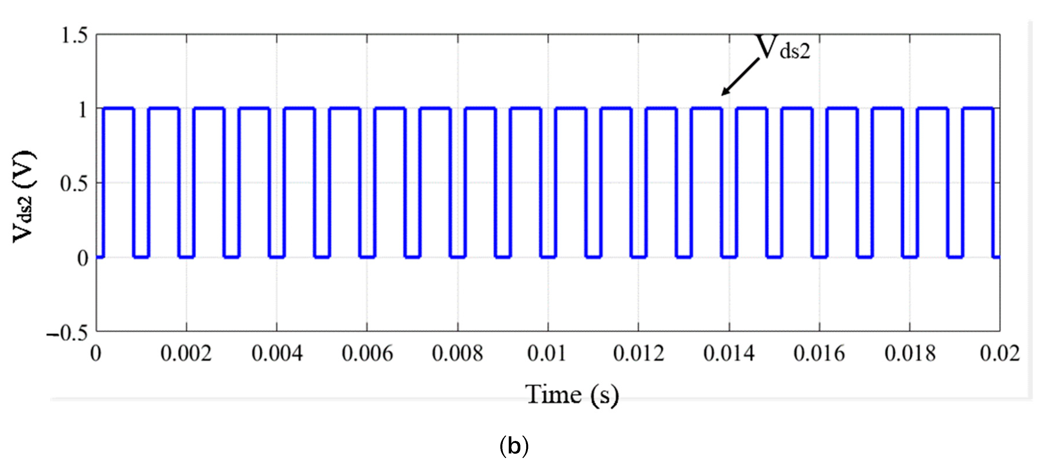
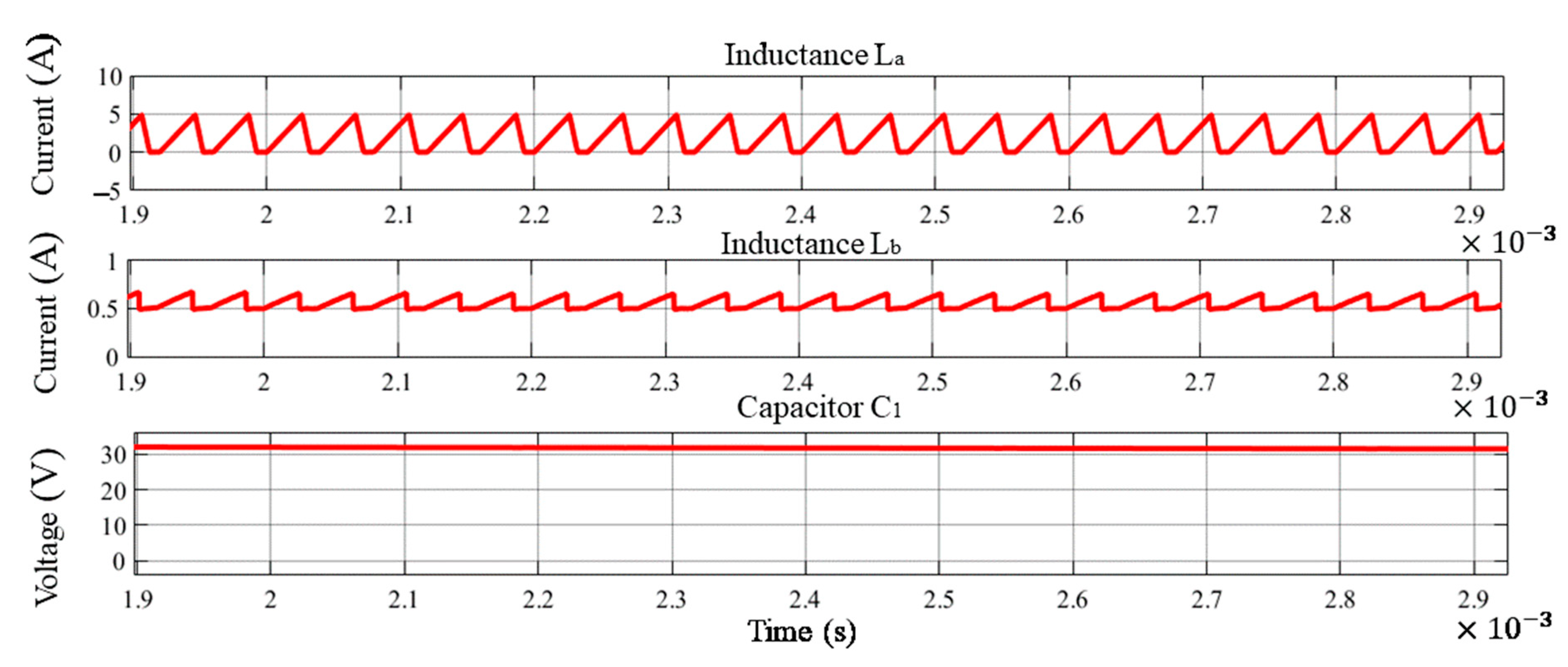
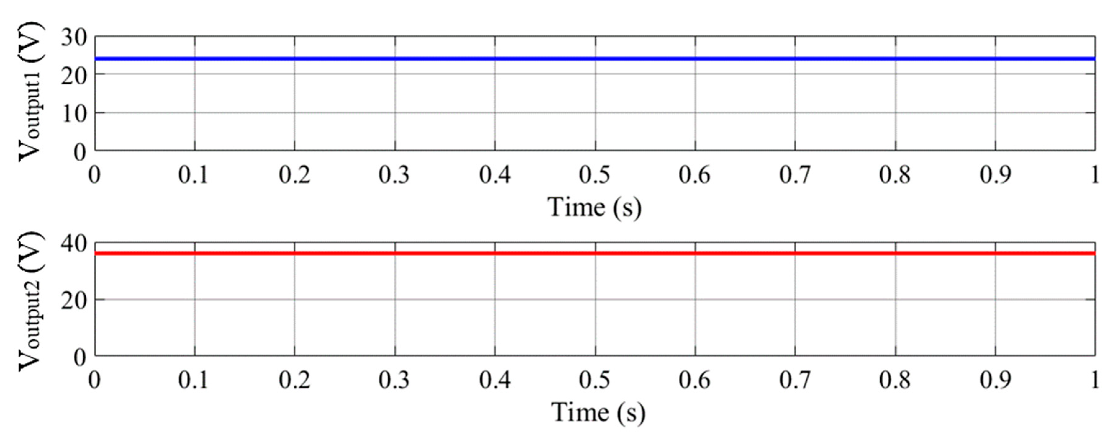
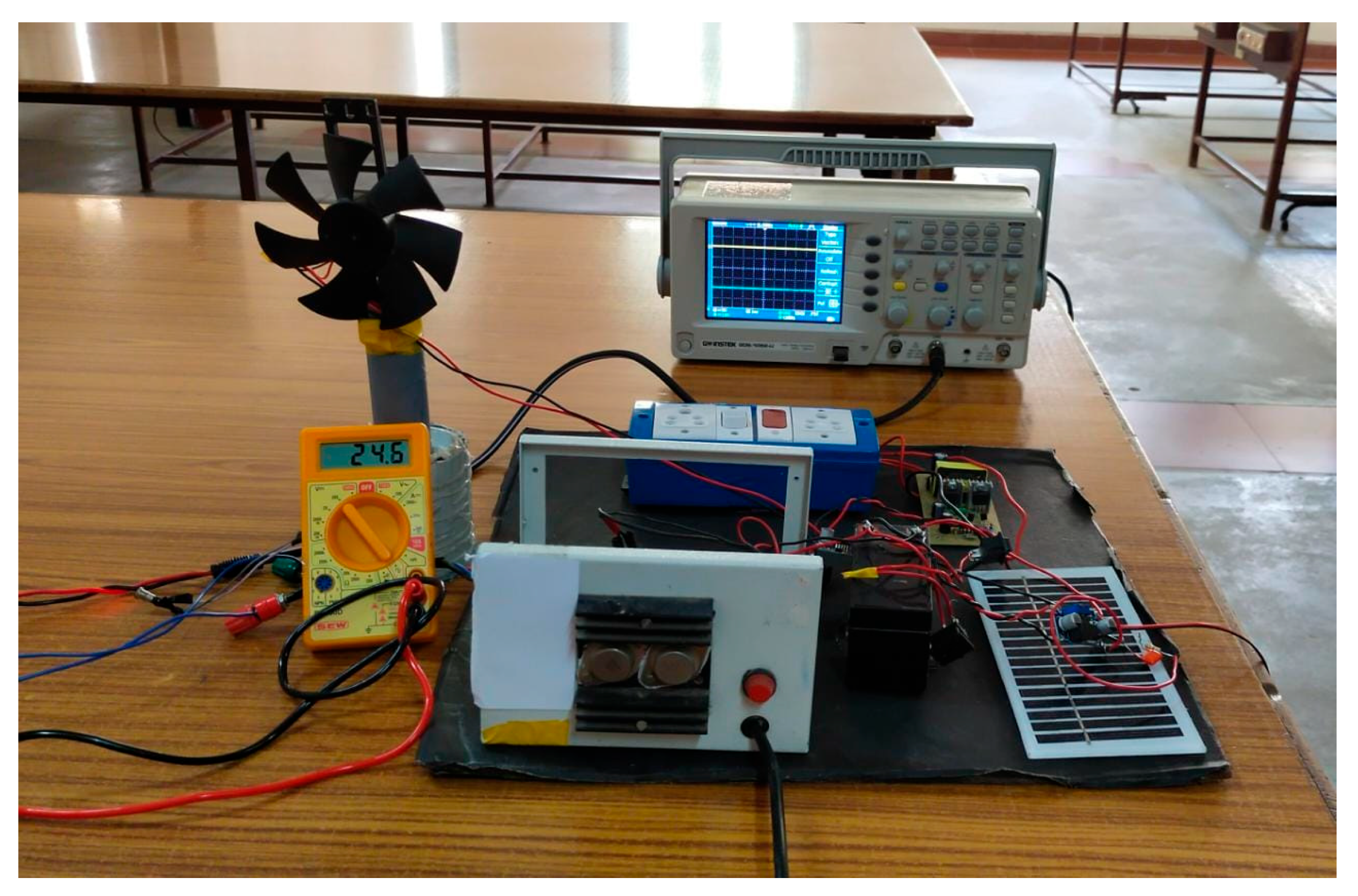
Experimental Results
5. Discussion
6. Conclusions
Author Contributions
Funding
Institutional Review Board Statement
Informed Consent Statement
Data Availability Statement
Acknowledgments
Conflicts of Interest
References
- Saadatizadeh, Z.; Heris, P.C.; Mantooth, H.A. Modular expandable multiinput multioutput (MIMO) high step-up transformerless DC–DC converter. IEEE Access 2022, 10, 53124–53142. [Google Scholar] [CrossRef]
- Shayeghi, H.; Pourjafar, S.; Hashemzadeh, S.M.; Sedaghati, F. Presenting of the magnetic coupling-based transformer-less high step-up DC-DC converter for Renewable Energy Applications. Int. Trans. Electr. Energy Syst. 2022, 2022, 3141119. [Google Scholar] [CrossRef]
- Madhana, R.; Mani, G. Power enhancement methods of renewable energy resources using multiport DC-DC converter: A technical review. Sustain. Comput. Inform. Syst. 2022, 35, 100689. [Google Scholar] [CrossRef]
- Bahrami, H.; Allahyari, H.; Adib, E. An improved wide ZVS soft-switching range PWM bidirectional forward converter for low power applications with simple control circuit. IET Power Electron. 2022, 1–12. [Google Scholar] [CrossRef]
- Appikonda, M.; Dhanalakshmi, K. Small-signal model and control approach for a dual input boost converter with VMC. Int. J. Electron. 2021, 109, 1035–1058. [Google Scholar] [CrossRef]
- Ahmad, F.; Haider, A.A.; Naveed, H.; Mustafa, A.; Ahmad, I. Multiple input multiple output DC to DC converter. In Proceedings of the 2018 5th International Multi-Topic ICT Conference (IMTIC), Jamshoro, Pakistan, 25–27 April 2018. [Google Scholar]
- Li, X.L.; Tse, C.K.; Lu, D.D.-C. Synthesis of reconfigurable and scalable single-inductor multiport converters with no cross regulation. IEEE Trans. Power Electron. 2022, 37, 10889–10902. [Google Scholar] [CrossRef]
- Malik, M.Z.; Chen, H.; Nazir, M.S.; Khan, I.A.; Abdalla, A.N.; Ali, A.; Chen, W. A new efficient step-up boost converter with CLD cell for electric vehicle and New Energy Systems. Energies 2020, 13, 1791. [Google Scholar] [CrossRef] [Green Version]
- Shoaei, A.; Abbaszadeh, K.; Allahyari, H. A single-inductor multi-input multi-level high step-up DC-DC converter based on switched-diode-capacitor cells for PV applications. IEEE J. Emerg. Sel. Top. Ind. Electron. 2022. [Google Scholar] [CrossRef]
- Dhimish, M.; Schofield, N. Single-Switch Boost-Buck DC-DC converter for industrial fuel cell and photovoltaics applications. Int. J. Hydrogen Energy 2022, 47, 1241–1255. [Google Scholar] [CrossRef]
- Azmoon-Asmarood, S.; Maalandish, M.; Shoghli, I.; Nazemi-Oskuee, S.H.; Hosseini, S.H. A non-isolated high step-up MIMO DC–DC converter for renewable energy applications. IET Power Electron. 2022, 15, 962–963. [Google Scholar] [CrossRef]
- Mishra, S.K.; Nayak, K.K.; Rana, M.S.; Dharmarajan, V. Switched-boost action based Multiport Converter. IEEE Trans. Ind. Appl. 2019, 55, 964–975. [Google Scholar] [CrossRef]
- Saadatizadeh, Z.; Heris, P.C.; Babaei, E.; Sabahi, M. A new nonisolated single-input three-output high voltage gain converter with low voltage stresses on switches and diodes. IEEE Trans. Ind. Electron. 2019, 66, 4308–4318. [Google Scholar] [CrossRef]
- Keyhani, H.; Toliyat, H.A. A ZVS single-inductor multi-input multi-output DC-DC converter with the step up/down capability. In Proceedings of the 2013 IEEE Energy Conversion Congress and Exposition, Denver, CO, USA, 15–19 September 2013. [Google Scholar] [CrossRef]
- Gupta, J.; Singh, B. Bridgeless isolated positive output Luo converter based high power factor single stage charging solution for Light Electric Vehicles. IEEE Trans. Ind. Appl. 2022, 58, 732–741. [Google Scholar] [CrossRef]
- Wang, B.; Xian, L.; Kanamarlapudi, V.R.; Tseng, K.J.; Ukil, A.; Gooi, H.B. A digital method of power-sharing and cross-regulation suppression for single-inductor multiple-input multiple-output DC–DC converter. IEEE Trans. Ind. Electron. 2017, 64, 2836–2847. [Google Scholar] [CrossRef]
- Gorji, S.A.; Sahebi, H.G.; Movahed, M.; Ektesabi, M. Multi-input Boost DC-DC converter with continuous input-output current for Renewable Energy Systems. In Proceedings of the 2019 IEEE 4th International Future Energy Electronics Conference (IFEEC), Singapore, 25–28 November 2019. [Google Scholar]
- Ramu, S.K.; Paramasivam, S.; Muthusamy, S.; Panchal, H.; Sadasivuni, K.K.; Noorollahi, Y. A novel design of switched boost action based multiport converter using dsPIC controller for Renewable Energy Applications. Energy Sources Part A Recovery Util. Environ. Eff. 2021, 44, 75–90. [Google Scholar] [CrossRef]
- Williams, B.W. DC-to-DC converters with continuous input and output power. IEEE Trans. Power Electron. 2019, 28, 2307–2316. [Google Scholar] [CrossRef]
- Wang, B.; Zhang, X.; Ye, J.; Gooi, H.B. Deadbeat control for a single-inductor multiple-input multiple-output DC–DC converter. IEEE Trans. Power Electron. 2019, 34, 1914–1924. [Google Scholar] [CrossRef]
- Li, Y.; Han, Y. A module-integrated distributed Battery Energy Storage and Management System. IEEE Trans. Power Electron. 2016, 31, 8260–8270. [Google Scholar] [CrossRef]
- Li, X.L.; Dong, Z.; Tse, C.K. Complete family of two-stage single-input multioutput configurations of interconnected power converters. IEEE Trans. Power Electron. 2010, 35, 3713–3728. [Google Scholar] [CrossRef]
- Saadatizadeh, Z.; Chavoshipour Heris, P.; Babaei, E.; Blaabjerg, F.; Cecati, C. Sido coupled inductor-based high voltage conversion ratio DC–DC converter with three operations. IET Power Electron. 2021, 14, 1735–1752. [Google Scholar] [CrossRef]
- Hou, S.; Chen, J.; Sun, T.; Bi, X. Multi-input step-up converters based on the switched-diode-capacitor voltage accumulator. IEEE Trans. Power Electron. 2016, 31, 381–393. [Google Scholar] [CrossRef]
- Nahavandi, A.; Hagh, M.T.; Sharifian, M.B.; Danyali, S. A nonisolated multiinput multioutput DC–DC boost converter for Electric Vehicle Applications. IEEE Trans. Power Electron. 2015, 30, 1818–1835. [Google Scholar] [CrossRef]
- Varesi, K.; Hossein Hosseini, S.; Sabahi, M.; Babaei, E.; Saeidabadi, S.; Vosoughi, N. Design and analysis of a developed multiport high step-up DC–DC converter with reduced device count and normalized peak inverse voltage on the switches/diodes. IEEE Trans. Power Electron. 2019, 34, 5464–5475. [Google Scholar] [CrossRef]
- Deihimi, A.; Seyed Mahmoodieh, M.E.; Iravani, R. A new multi-input step-up DC–DC converter for Hybrid Energy Systems. Electr. Power Syst. Res. 2017, 149, 111–124. [Google Scholar] [CrossRef]
- Li, X.L.; Dong, Z.; Tse, C.K.; Lu, D.D.-C. Single-inductor multi-input multi-output DC–DC converter with high flexibility and simple control. IEEE Trans. Power Electron. 2020, 35, 13104–13114. [Google Scholar] [CrossRef]
- Pourjafar, S.; Sedaghati, F.; Shayeghi, H.; Maalandish, M. High step-up DC–DC converter with coupled inductor suitable for renewable applications. IET Power Electron. 2019, 12, 92–101. [Google Scholar] [CrossRef]
- Samanes, J.; Urtasun, A.; Barrios, E.L.; Lumbreras, D.; Lopez, J.; Gubia, E.; Sanchis, P. Control Design and Stability Analysis of power converters: The MIMO generalized Bode Criterion. IEEE J. Emerg. Sel. Top. Power Electron. 2020, 8, 1880–1893. [Google Scholar] [CrossRef]


| Parameters | Symbol | Value |
|---|---|---|
| Input Voltages | 5 V | |
| 12 V | ||
| Output Voltages | 24 V | |
| 36 V | ||
| Capacitors | C1 | 6.4 µF |
| C2 | 4 µF | |
| C3 | 4 µF | |
| Inductors | La | 0.225 µH |
| Lb | 0.8 µH | |
| Lc | 0.8 µH | |
| Load Resistance | R1 | 10 Ω |
| R2 | 15 Ω | |
| Duty Cycle | D1 | 0.79 |
| D2 | 0.67 | |
| Switching Frequency | Fs | 25,000 Hz |
| Ref. | Converter Type | Number of Switches | IV | OV | PD | EC | Stability | Efficiency | Observations | ||||
|---|---|---|---|---|---|---|---|---|---|---|---|---|---|
| D | C | S | L | Outputs | |||||||||
| [1] | MIMO high step-up transformerless converter | 4 | 3 | 4 | 1 | 2 | 30 V, 20 V | 21 V, 8 V | Medium | Medium | NR | 93.98 | Hybrid energy sources integration and MO |
| [8] | Step-up boost converter with CLD cell | 1 | 5 | 2 | 2 | 2 | 34 V, 48 V | 80 V, 40 V | Medium | Medium | NR | 93.4 | high voltage gain without maximum value of duty cycle |
| [12] | Switching boosting action-based MIMO converter | 3 | 5 | 4 | 1 | 2 | 25 V, 20 V | 22 V, 11 V | High | Low | NR | 92.1 | Improve the power density in various load applications |
| [16] | Single-inductor MIMO converter | 4 | 3 | 4 | 2 | 1 | 24 V, 20 V | 12 V, 8 V | Medium | Low | NR | 89.7 | Integration of various loads with minimum number of components |
| [28] | Single-inductor–multi-input–multi-output DC–DC converter | 4 | 3 | 4 | 1 | 3 | 18 V, 22 V | 12 V, 8 V | Low | Medium | NR | 91.5 | Integration of multiple loads with fixed current control |
| Proposed Work | High step-up MIMO Converter with low power losses | 2 | 3 | 2 | 3 | 2 | 5 V, 12 V | 24 V, 36 V | High | High | Reported | 94.3 | Tarnsformerless MIMO converter with fewer number of switches |
Publisher’s Note: MDPI stays neutral with regard to jurisdictional claims in published maps and institutional affiliations. |
© 2022 by the authors. Licensee MDPI, Basel, Switzerland. This article is an open access article distributed under the terms and conditions of the Creative Commons Attribution (CC BY) license (https://creativecommons.org/licenses/by/4.0/).
Share and Cite
Aljafari, B.; Ramu, S.K.; Devarajan, G.; Vairavasundaram, I. Integration of Photovoltaic-Based Transformerless High Step-Up Dual-Output–Dual-Input Converter with Low Power Losses for Energy Storage Applications. Energies 2022, 15, 5559. https://doi.org/10.3390/en15155559
Aljafari B, Ramu SK, Devarajan G, Vairavasundaram I. Integration of Photovoltaic-Based Transformerless High Step-Up Dual-Output–Dual-Input Converter with Low Power Losses for Energy Storage Applications. Energies. 2022; 15(15):5559. https://doi.org/10.3390/en15155559
Chicago/Turabian StyleAljafari, Belqasem, Senthil Kumar Ramu, Gunapriya Devarajan, and Indragandhi Vairavasundaram. 2022. "Integration of Photovoltaic-Based Transformerless High Step-Up Dual-Output–Dual-Input Converter with Low Power Losses for Energy Storage Applications" Energies 15, no. 15: 5559. https://doi.org/10.3390/en15155559