
Magnetic Functionalization of Scanning Probes by Focused Electron Beam Induced Deposition Technology
by
 , ,
, ,
Javier Pablo-Navarro
1,2,3,* ,
,
Soraya Sangiao
2,3,4,
César Magén
2,3,4 and
José María de Teresa
2,3,4 1
Institute of Ion Beam Physics and Materials Research, Helmholtz-Zentrum Dresden-Rossendorf, 01328 Dresden, Germany
2
Instituto de Nanociencia y Materiales de Aragón (INMA), Universidad de Zaragoza-CSIC, 50009 Zaragoza, Spain
3
Laboratorio de Microscopías Avanzadas (LMA), Universidad de Zaragoza, 50018 Zaragoza, Spain
4
Departamento de Física de la Materia Condensada, Universidad de Zaragoza, 50009 Zaragoza, Spain
*
Author to whom correspondence should be addressed.
Magnetochemistry 2021, 7(10), 140; https://doi.org/10.3390/magnetochemistry7100140
Submission received: 11 September 2021
/
Revised: 1 October 2021
/
Accepted: 9 October 2021
/
Published: 13 October 2021
(This article belongs to the Special Issue Advances in Magnetic Force Microscopy)
Abstract
:The fabrication of nanostructures with high resolution and precise control of the deposition site makes Focused Electron Beam Induced Deposition (FEBID) a unique nanolithography process. In the case of magnetic materials, apart from the FEBID potential in standard substrates for multiple applications in data storage and logic, the use of this technology for the growth of nanomagnets on different types of scanning probes opens new paths in magnetic sensing, becoming a benchmark for magnetic functionalization. This work reviews the recent advances in the integration of FEBID magnetic nanostructures onto cantilevers to produce advanced magnetic sensing devices with unprecedented performance.
1. Introduction to FEBID and MFM
Focused Electron Beam Induced Deposition (FEBID) is one of the most versatile and promising technologies for the fabrication of nanostructures, emerging as a complementary technique to existing fabrication methods. This single-step nanolithography process, first introduced by S. Matsui in 1984 [1], relies on the decomposition by a finely-focused electron beam of the molecules of a precursor gas on a substrate, eventually producing a solid deposit [2,3,4,5]. The precursor molecules are delivered locally over the substrate by a gas injection system (GIS) and adsorbed on the surface, some of them being dissociated by the electron beam into volatile and non-volatile parts. The non-volatile part of the gas is deposited whereas the volatile one is pumped out of the working chamber. The shape of the deposit is determined by the electron beam scan pattern, and the interactions between the electron beam, substrate, precursor gas molecules, and the growing structure [6,7]. The diffusion, adsorption, and desorption phenomena of the gas molecules on top of the substrate and the probability of the secondary electrons generated to break the molecules bonds are crucial in this nanofabrication process. FEBID has demonstrated to be remarkably successful in growing nanometer-scale objects and devices with 2D and 3D geometries [8,9,10,11,12,13,14,15,16,17,18], providing the possibility to pattern architectures with high lateral resolution and on unconventional surfaces. The technique is nurtured by an extensive catalogue of precursors that enable the deposition of an ever-growing number of materials and compounds, with a great variety of physical properties, such as metallicity and magnetoresistance [2], insulating behavior [19], superconductivity [20], ferromagnetism and superparamagnetism [21,22], or plasmonic behavior [23], among others.
Specifically, it is worth stressing the use of precursor gas molecules containing magnetic elements, such as Co, Fe and Ni [21,24,25,26,27,28,29,30], which has allowed a significant progress towards the growth of complex-shaped magnetic deposits with high metallic content and magnetization, as recently reviewed [31,32]. This development has been focused on the optimization of thin magnetic patterns in 2D. More recently, the investigation has been extended to 3D FEBID magnetic deposits [33,34,35], spurred on by promising applications in scanning probe techniques, such as Magnetic Force Microscopy (MFM) [36] and Magnetic Resonance Force Microscopy (MRFM) [37], racetrack-type magnetic memories [14], Hall sensors [11,22], nanomagnetic logic circuits [36,38], superconducting vortex lattice pinning [39], remote magneto-mechanical actuation [40], etc. However, whereas FEBID flexibility allows the production of challenging structures with sophisticated geometries [7,10,12], many applications can be based on the simplest objects, such as vertical straight nanowires.
MFM is one of the most common techniques used in research and industry for the characterization of magnetic properties at the nanoscale. To show the potential for the integration of 3D FEBID ferromagnetic nanostructures in MFM probes, the use of vertical magnetic nanowires [41,42] to functionalize Atomic Force Microscopy (AFM) tips is reviewed here. Specifically, this combination has been found to improve the performance of the standard magnetic tips and further progress could have a significant impact in this field. Based on this concept, the utilization of nanometer-scale force transducers to map with high resolution and sensitivity the magnetic fields of the sample (rather than magnetic field gradients) in scanning nanowire magnetic force sensing [43,44] is also discussed. Finally, the growth of magnetic nanocubes and nanospheres on AFM tips is analyzed as an application to enhance the performance of MRFM measurements, taking advantage of the tip–sample interaction for the investigation of spin dynamics [45].
MFM relies on the long-range magnetostatic force between a magnetic sample and a magnetic probe [46]. The MFM contrast is proportional to the magnetic pole density at the surface of the magnetic specimen. Therefore, samples with either perpendicular or in-plane anisotropy can be studied, where the poles are located at the domains or at the domain walls, respectively [46]. The sensitivity, defined by the minimum detectable change of the frequency shift, , [47] and the spatial resolution, which can reach values of ~10 nm under optimum conditions [48,49], are limited by different factors such as the tip–sample distance, the magnetized volume of the tip, the type of cantilever, the tip magnetic moment, etc. To enhance the MFM performance, some technical limitations, such as the non-magnetic interactions between the tip and the sample, should be considered in order to ensure a high magnetic signal-to-noise ratio. Similarly, the characterization could be improved by reducing the magnetic invasiveness. Additionally, improving the lateral resolution obtained with the current MFM tips would lead to cutting-edge investigations in magnetism.
Diverse approaches have been taken to improve the performance of MFM tips [50,51,52]. The coating with magnetic material of nano-objects located in the apex, such as C nanotubes [53], the growth of magnetic nanowires by electrodeposition [54], or the use of nanoscale magnets sharpened by Focused Ion Beam milling [55] are strategies to reduce the magnetic material of the probe and consequently optimize the MFM signal. However, these procedures have not resulted in an improvement of the technique. In view of this, the development of new systems or refinements of the current sensing devices [21,36] are required to provide an upgraded and robust measurement method.
This situation has triggered the growth of materials in the form of vertical nanowires by FEBID as magnetic probes onto AFM cantilevers. A proof-of-concept was demonstrated for the first time by growing high-aspect-ratio ferromagnetic Co nanowires and analyzing the tip performance in hard disks reference samples [21,56]. A few years later, the prevailing spatial magnetic resolution of ~40 nm was improved down to 10 nm by growing higher purity ferromagnetic Co-FEBID nanowires with thinner diameters [48]. Additionally, Fe-based deposits were grown on AFM tips correcting the angle formed with respect to the target sample, inducing an accurate MFM measurement of 3D nanomagnet logic arrays [36]. These pioneering studies pointed out that, due to the high aspect ratio, high coercivity, small lateral dimensions, and the precise control of the deposition location, magnetic FEBID nanowires grown on standard AFM probes are perfect candidates for working as MFM tips [54,57].
Further efforts to optimize their performance have been reported [58]. In particular, 3D Co and Fe nanowires were grown on various kinds of tips and under different growth conditions, characterized magnetically, and tested in different environments to compare their operational performance with that of commercial MFM probes. It was recently shown that tailored FEBID tips are superior to standard MFM ones in certain applications and can give rise to a new generation of commercial MFM tips [41]. Furthermore, the use of these refined MFM tips for studies in non-standard environments such as liquid media could actively prompt the detection of new phenomena [47]. Moreover, FEBID tips may even be used in self-sensing cantilevers, which integrate piezoresistors for non-optical detection that would suffer from electrical shortcut due to magnetic coating [59].
2. Magnetic Force Microscopy Using Tips Grown by FEBID
2.1. Growth and Properties of MFM Tips Grown by FEBID
The different geometries of the commercial probes—the most typical ones being pyramidal and cone-shaped— require a very sharp tip, i.e., a small radius of curvature at the apex, to ensure a good spatial resolution both in AFM and MFM measurements. Although the sensitivity and resolution are also limited by the mechanical properties of the cantilever and the control electronics, in the MFM case, the magnetic stray field of the tip is a key parameter. This can be controlled by the modification of the final architecture of the probes, customizing their magnetic behavior. Particularly, the modulation of the general aspect ratio and the diameter and shape of the 3D ferromagnetic nanowires at the very end of the nanowire tip can be carried out by FEBID. This possibility breaks new ground in the degree of control in the functionalization of MFM probes.
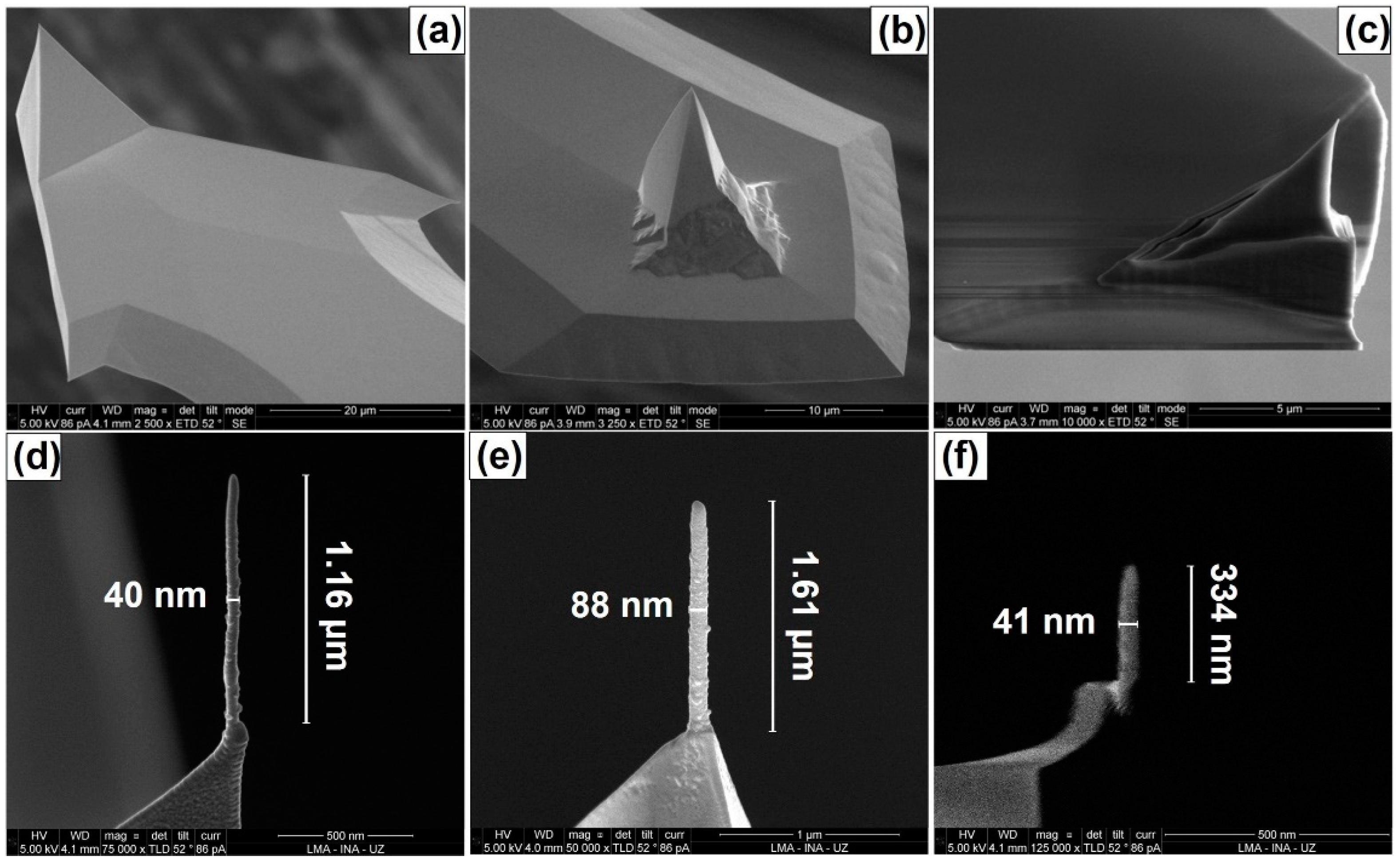
The growth of FEBID nano-objects on the apex of AFM tips requires an accurate electron beam aberration correction, and a proper charge dissipation during FEBID growth on the tips would be advisable. For instance, Nanoworld ArrowTM EFM, Budget Sensors® ElectriMulti75-G, and Bruker probes, as well as tips with strong charging effect such as Olympus BioLever mini have been proven to be useful, as reported by Jaafar et al. [41]. The small deposition surface compared to conventional flat substrates reduces the number of molecules available for decomposition. Under this situation, the angle of the GIS needle with respect to the horizontal axis becomes increasingly important as it determines the gas flow quantity [60]. Furthermore, the probe geometry also has a negative impact on heat dissipation, promoting greater nanowire diameters as the temperature increases, especially when working at low voltages (~3–5 kV). Nonetheless, this factor also contributes to increase the metallic purity up to 80 at. % in Co and Fe deposits. Likewise, the control of the length and the diameter is entirely possible while keeping the voltage constant, mainly through the deposition time and the electron beam current. Specifically, the reduction of the nanowire diameter is linked to a decrease of the beam current. Figure 1d–f illustrates the growth of 3D Co and Fe nanowires at low voltages on different types of probes with diameters ranging from 40 nm to 90 nm. Even though Scanning Electron Microscopy (SEM) lateral resolution is below 1 nm, FEBID deposits with such dimensions cannot be fabricated due to the much larger interaction volume generated by the electron beam. As a result, nanostructures with sub-100 nm resolution are typically achieved.
The coercive field of the FEBID tips reaches 55–60 mT, under external magnetic fields applied parallel to the nanowire long axis. In comparison, the commercial MFM tips show experimental values of 20 mT (Team Nanotec) and 35 mT (Budget Sensors®). Hence, FEBID tips are more robust upon contrast inversion due to magnetization reversal of the tip caused by the stray magnetic field generated by the sample.
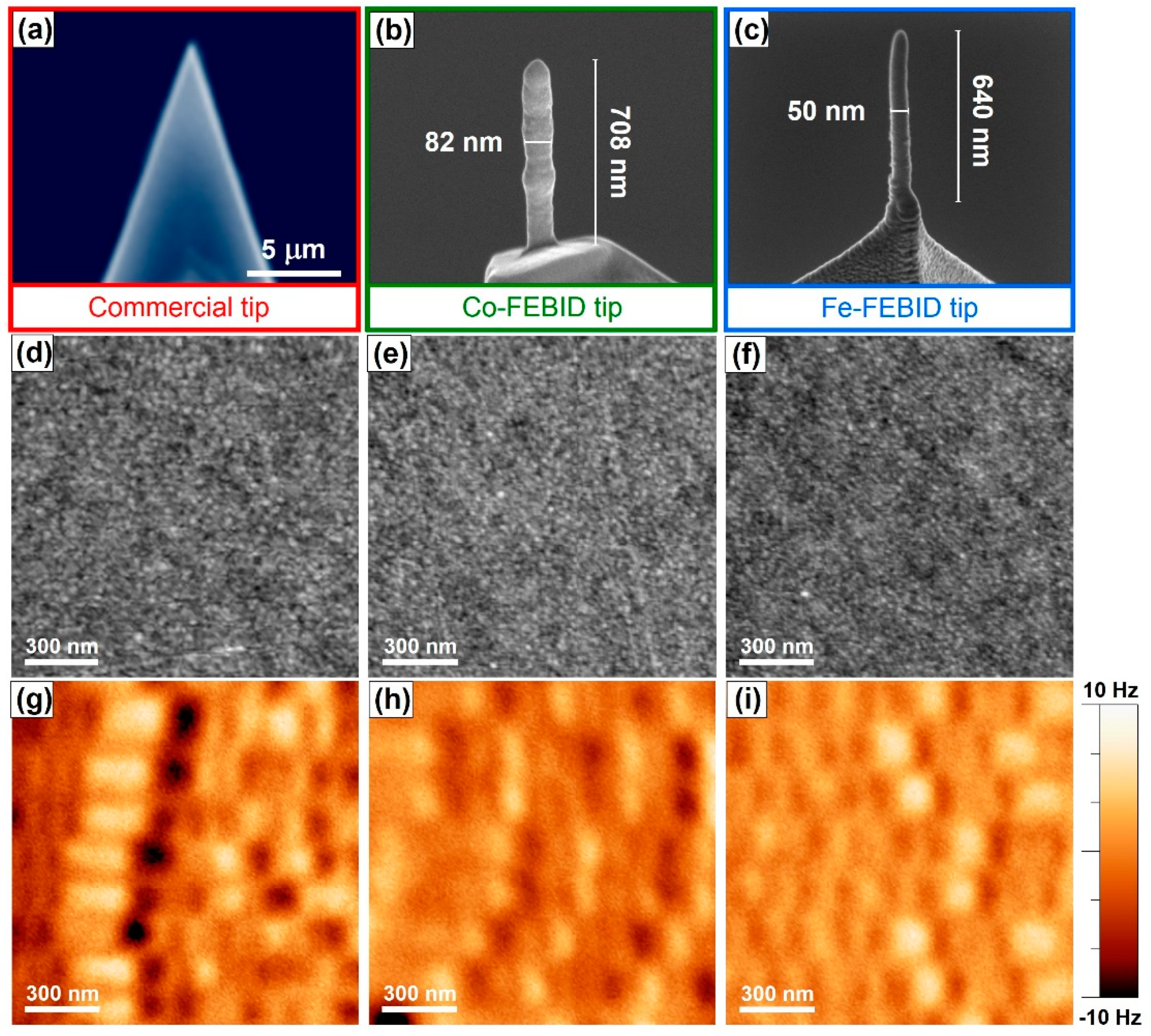
On the other hand, the sensitivity and image contrast can be compared using a high-density hard disk as a reference sample. Figure 2 shows similar performance for commercial and FEBID tips [41]. However, it should be emphasized that the possibility of tuning the magnetic properties of FEBID tips is an advantage for high-performance MFM operation.
As illustrated in Figure 3, FEBID nanowires with different properties can be grown onto AFM probes. For example, either nanowires with extremely thin diameter or very sharp tip ends [42] or core-shell architectures to avoid the surface oxidation of the magnetic core to a non-ferromagnetic material, which degrades the magnetic properties [62]. Nonetheless, achieving the narrowest diameters with high metallic content (and magnetization) is not possible, being necessary to reach a trade-off between dimensions and composition [63]. Indeed, some studies have been devoted to determining the relationship between FEBID chemical composition, especially in Co, and the electron beam voltage and current [24,64], precursor gas flux [11], patterning parameters [65], substrate temperature [64], etc. In the case of Fe, even with a precise control of the growth parameters, the 3D as-grown materials present a moderate purity which can be increased by annealing treatments [25,66,67]. Moreover, performing future quantitative MFM studies is a potential advantage of FEBID tips, since the extraction of magnetic quantitative information is one of the major challenges for the future progress in MFM, which requires tips with well-defined physical properties [68].
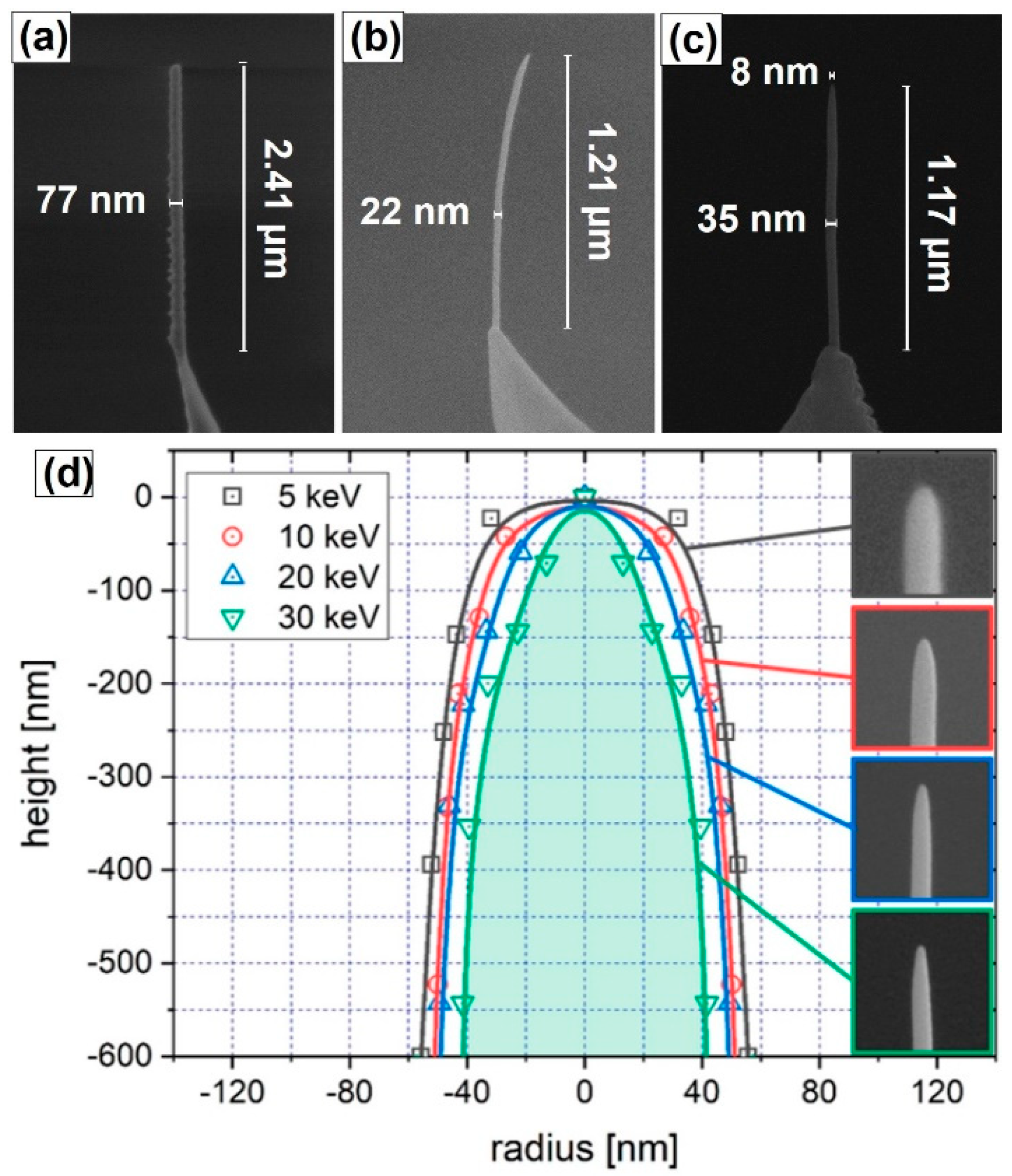
One of the fundamental principles of SEM image resolution consists of the fact that the higher the accelerating voltage is, the better the resolution of the image becomes. This also works for the FEBID fabrication process, where the thinnest nanowires can be grown at the highest accelerating voltages. According to Figure 3d, the shape of the tip end replicates the top part of the electron beam interaction volume in the deposit [69]. Therefore, the shape of the nanowire tip end can be modulated by tuning the accelerating voltage. The upper nanowire part presents a blunt shape when using voltage values in the range 3–5 kV, as illustrated in Figure 3a; however, it exhibits a smaller diameter and an extremely pointy end at 30 kV. These features can be appreciated in the thinnest ferromagnetic nanowire ever grown by FEBID (~22 nm in diameter) [61] imaged in Figure 3b and, more precisely, in the example of the nanowire routinely grown under these conditions, shown in Figure 3c. In this case, an overall diameter of around 35 nm as well as a ~8 nm-wide tip were obtained with high reproducibility. This novel shape configuration is very useful to perform very high resolution MFM imaging as well as to obtain relatively low tip–sample interaction, minimizing the influence of the tip on the magnetic state of the sample structures [42].
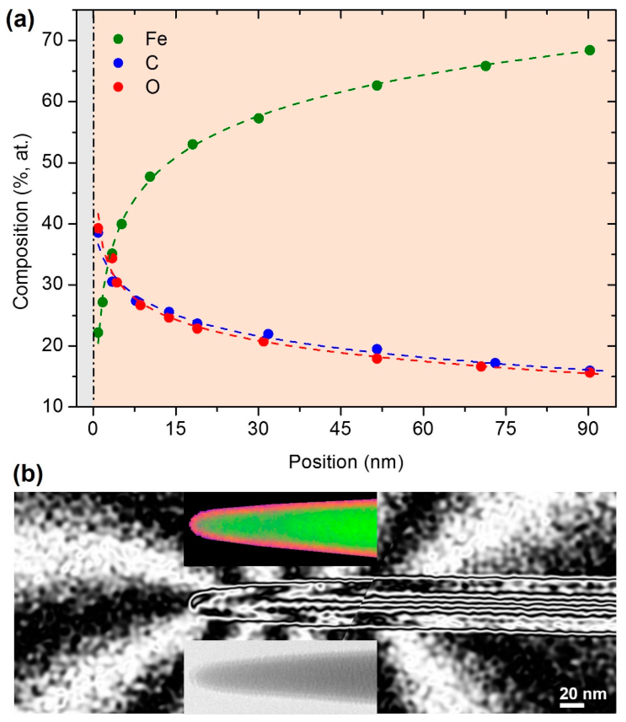
A local characterization of these tips was recently performed by Scanning Transmission Electron Microscopy-Electron Energy Loss Spectroscopy (STEM-EELS) chemical analyses. A metallic content of ~80 at. % was obtained in the FEBID probes with the best signal-to-noise ratio [42]. As illustrated in Figure 4a, the compositional profile along the length of the nanowire as a function of the distance to the tip end reveals that the Fe content decreases as the tip end is approached. As expected, the higher contribution of the oxidation layer at the tip end justifies the Fe drop from ~70 at. % in the central region down to ~35 at. % at 3.5 nm from the tip, which corresponds with the thickness of the oxidation shell.
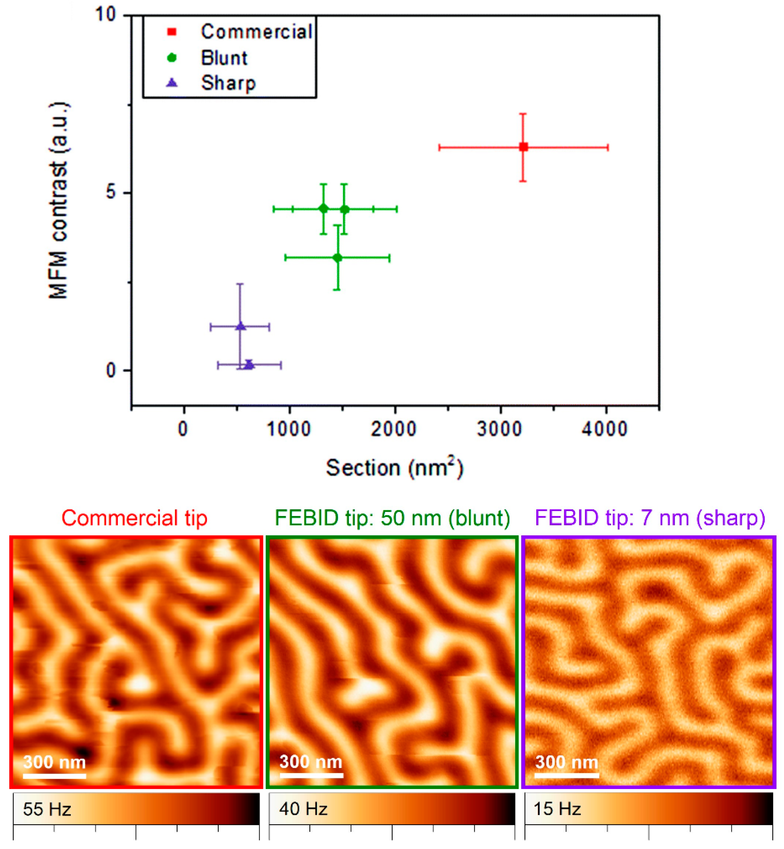
The magnetic characterization by electron holography, illustrated in Figure 4b, allows for mapping not only the magnetic induction () inside of the specimen (~1 T in the central region) but also the value of the magnetic stray field as a function of the distance to the tip end. This is particularly useful for the development of quantitative MFM measurements [70]. The magnetic flux lines indicate that the magnetization is high in the thick central part of the nanowire and decreases close to the narrow tip, giving rise to small stray fields. Therefore, the tip shape will have a significant impact in reducing the dipole magnetic interactions between the tip and the specimen. Jaafar et al. analyzed how the customization of the stray field by accurately controlling the nanowire tip dimensions impacts MFM experimental conditions [41]. As shown in Figure 5, the standard commercial MFM probes usually present frequency shifts around 55 Hz, which can be used to calculate when using a calibration sample. For comparison, two different FEBID nanowires with 1 µm in length and different diameters and tip end shapes were fabricated. The nanostructures with 50 nm in diameter and blunt shape showed frequencies shifts of ~40 Hz, whereas the nanowires with a sharp tip end of 7 nm exhibited ~15 Hz. This shows that the tailoring of the nanowire geometry can be used to adjust the tip–sample interaction.
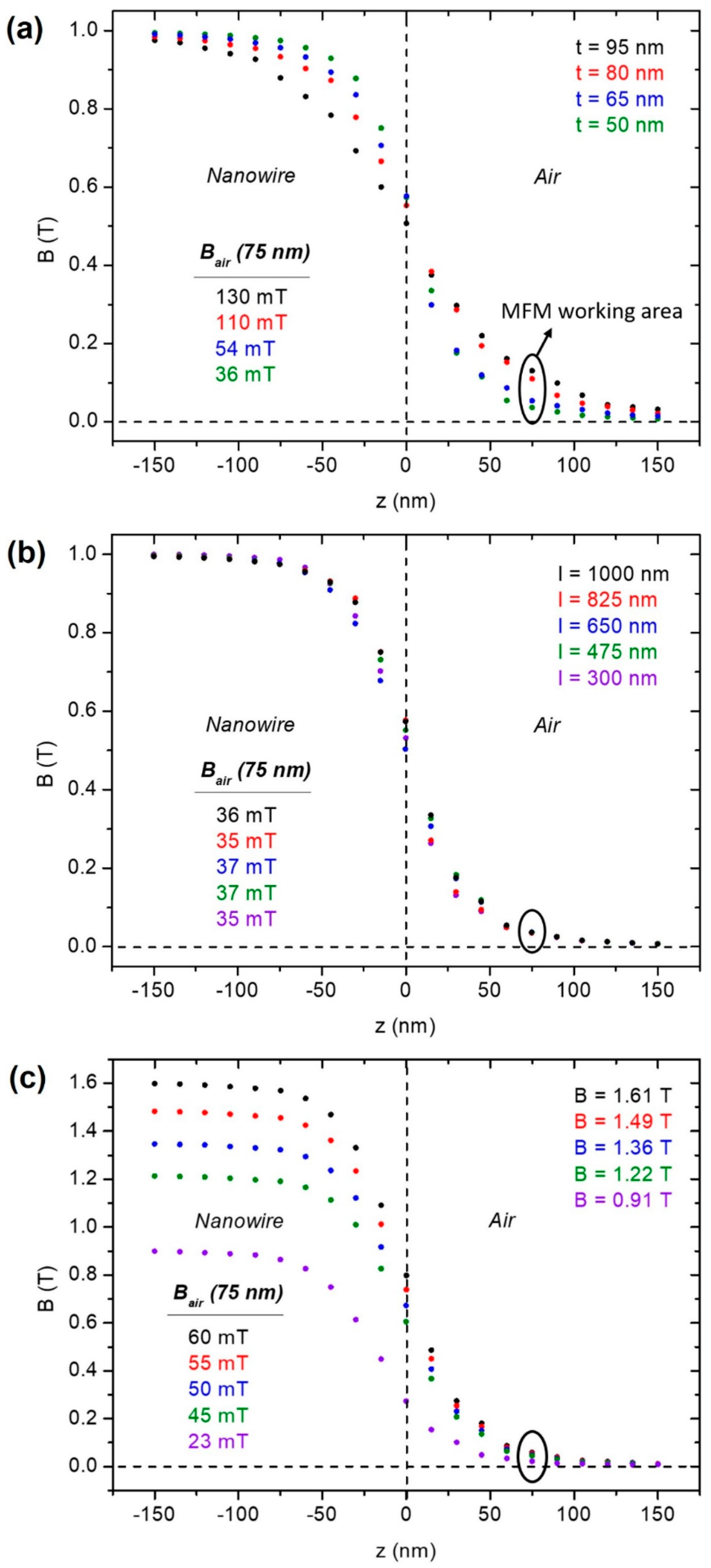
On the other hand, in order to provide a quantitative characterization of the magnetic stray fields, micromagnetic simulations were performed. Firstly, Figure 6a illustrates the variation of along the long axis of the nanowire depending on the nanostructure aspect ratio. Nanowires with 1 µm in length, diameters ranging from 50 nm to 95 nm and 1 T in the central region were modelled. An important difference in the magnetic signal can be appreciated at the estimated MFM working distance—around 75 nm far away from the tip— reducing the magnetic induction 3.5 times when decreasing the diameter by half. Secondly, the stray fields of 50-nm-wide nanowires were calculated as a function of the length, using values between 300 nm and 1 µm. In this case, the impact of the length of the nanowire is negligible in the MFM working distance, as shown in Figure 6b. Therefore, regarding the values of B for the MFM performance, the length of the nanowire is not as relevant as the diameter. This means that shorter nanowires can be used, which is an advantage concerning the fabrication time and their stability during MFM operation. Finally, in Figure 6c the evolution of as a function of the distance to the apex along the longitudinal axis direction for a nanowire of 750 nm in length and 50 nm in diameter is considered. As expected, the results indicate that, as decreases, the stray field value at the position of MFM operation decreases. More interestingly, at lower fields an increase of 30% of leads to an increase of the stray field by a factor of 2 in the MFM working area.
2.2. Detection of Soft Magnetic Textures
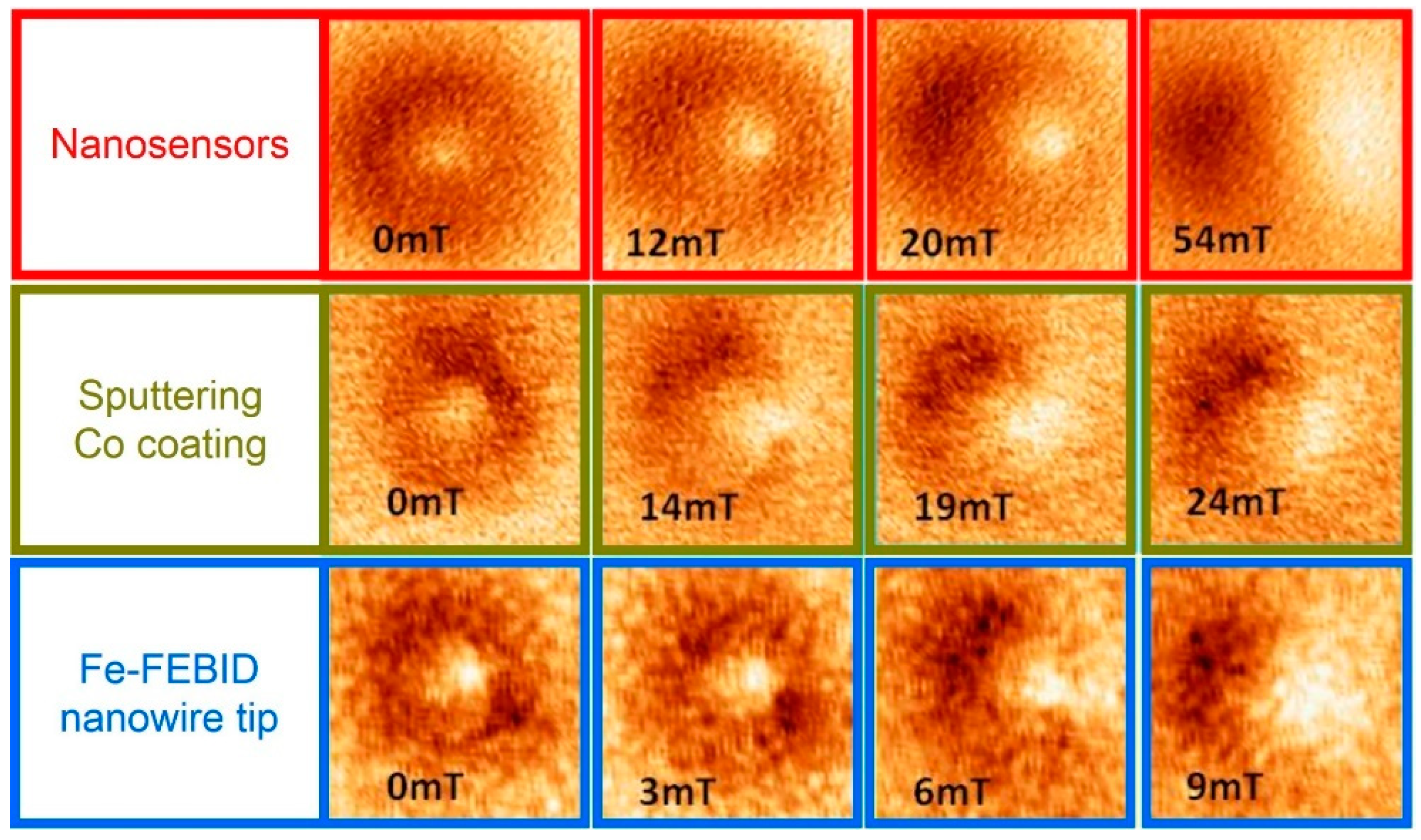
Berganza et al. recently reported the observation and stabilization of magnetic skyrmions by the magnetic field arisen from these functionalized tips [42]. In this study, the exploration of magnetic Néel half-hedgehog skyrmions was performed in soft magnetic polycrystalline permalloy nanodots with diameters below 100 nm by field-dependent MFM experiments with different magnetic probes [42]. As shown in Figure 7, an in-plane applied magnetic field changes the magnetic state of the nanostructure from the skyrmion configuration to the saturated one, but stability of the skyrmion state depends on the MFM tip used for imaging the process. The magnetic field required for saturation was the highest with the commercial NanosensorsTM probe, the Co-coated tip by sputtering offered an intermediate value, and the Fe-FEBID nanowire tip exhibited the lowest saturation field. This can be explained by the fact that the stray field coming from the MFM tip contributes to the stabilization of the skyrmions [71], being larger for the commercial probes. Consequently, the saturating field decreases as the generated stray field is reduced.
FEBID tips allow for imaging the skyrmions with better resolution and with the lowest invasiveness, maximizing the out-of-plane/in-plane (OOP/IP) stray field ratio. Since the application of OOP magnetic fields serves to tune the stability of the skyrmions, the FEBID nanolithography technique can modulate this stabilization by tuning the stray field values. Therefore, the use of FEBID functionalized probes is beneficial to analyze soft magnetic textures such as skyrmions without perturbating their magnetic state and to explore their magnetization dynamics.
2.3. Applications in Liquid Media
Many research lines rely on the investigation of samples which must remain in a liquid environment to be stabilized, e.g., culture media or dilutions. In these environments, the sensitivity is inversely proportional to the effective spring constant, , and heavily dependent on the quality factor, , which is linked to the damping coefficient and ultimately to the density of the liquid [47]. As a result, the signal-to-noise ratio is much worse in liquid media than in air conditions for the same cantilever. In order to improve the sensitivity, high resonance frequency and low are required [72], but a decrease implies a noise increment, proportional to .
Hereafter, an improved technology devoted to analyzing biological samples (cells, tissues, proteins, virus, bacteria, nucleic acids, etc.) with magnetic traces, nanoparticles, and nanowires is reviewed. These elements can act as contrast agents in nuclear magnetic resonance, heating elements in hyperthermia for cancer treatment, magnetic carriers for drug delivery, etc. Specifically, the magnetic properties which determine their effective implementation in biomedicine can be examined: magnetic domains configuration at remanence, magnetization reversal mechanism, stray fields, aggregate state of nanostructures in accordance with their size, level of material functionalization, and so on. For that purpose, the technological challenge of the observation and characterization of these magnetic samples in liquid media has been recently addressed using Co- and Fe-FEBID nanowire tips [41].
Figure 8 shows the results obtained on a hard disk in air and liquid conditions for commercial and FEBID tips. The use of a standard NanosensorsTM PPP-MFMR tip [47] demonstrates a clear deterioration of the signal-to-noise ratio in water environment, whereas the commercial Team Nanotec tip entails a stable, constant total signal-to-noise ratio in the liquid medium, with improved sensitivity and worse noise.
Given the performance constraints of the commercial probes, experiments with FEBID functionalized tips have been reported using dedicated cantilevers for working in liquid media. In particular, the Olympus BioLever mini AFM probe with a FEBID nanowire evidences a remarkable improvement of contrast and a strong noise reduction with respect to the standard commercial MFM tips in liquid. In fact, the image quality and sensitivity are approximately the same in both air and water, with the tip showing no aging effects after one year in storage.
3. Nanowire Magnetic Force Sensors
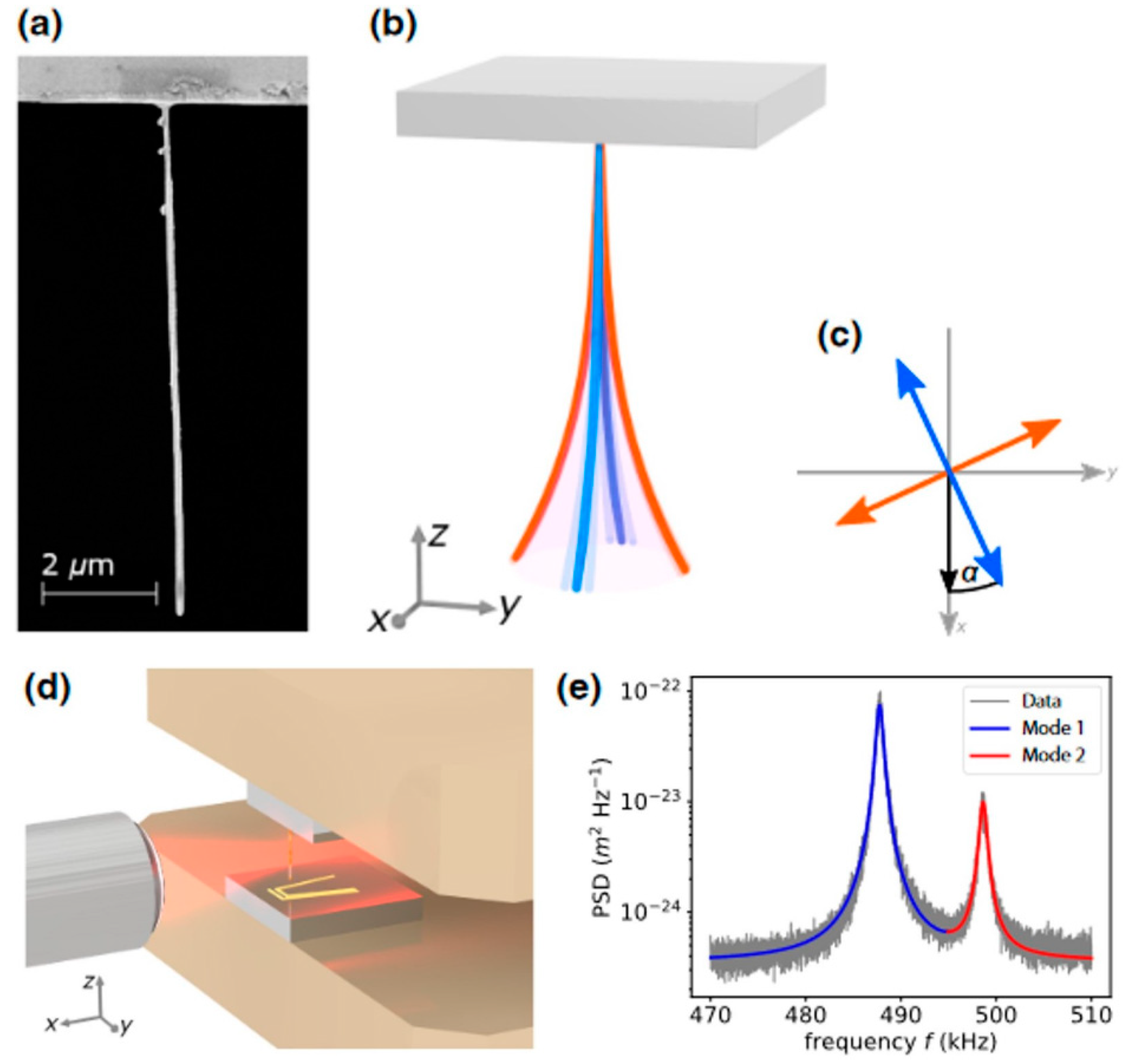
Magnetic nanowires have also been applied as scanning magnetic force microscopy sensors. Rossi et al. reported the use of GaAs nanowires with a single-crystalline MnAs magnetic tip [44]. The combination of the high force sensitivity and the small magnetic tip results in a potential tool for imaging weak magnetic field nano-patterns. More recently, Mattiat et al. showed a special type of MFM based on a transducer composed by a FEBID nanowire also acting as a local magnetic force sensor, with high-quality flexural mechanical modes, as shown in Figure 9. In particular, the growth of long Co-FEBID nanowires (~10 µm)—exhibiting 80 at. % of metallic purity and magnetic switching fields of around 40 mT—allows for very sensitive detection by means of dynamic cantilever magnetometry [43]. Due to the force interaction between the stray fields of the sample and the tip of the nanowire, different changes on the resonance frequency arise, which can be correlated to the flexural vibration modes of the long, mechanically stable nanowires. This design allows for reducing the invasiveness, favouring the mapping of magnetic fields of different magnetization textures with high resolution and sensitivity down to 3 nT·Hz1/2. This study also revealed that FEBID nanowires can be used as nanometer-scale force transducers, due to their high mechanical quality, and being sensitive to 2D lateral force and dissipation detection. In addition, this device has the potential capability for vectorial force sensing in 3D.
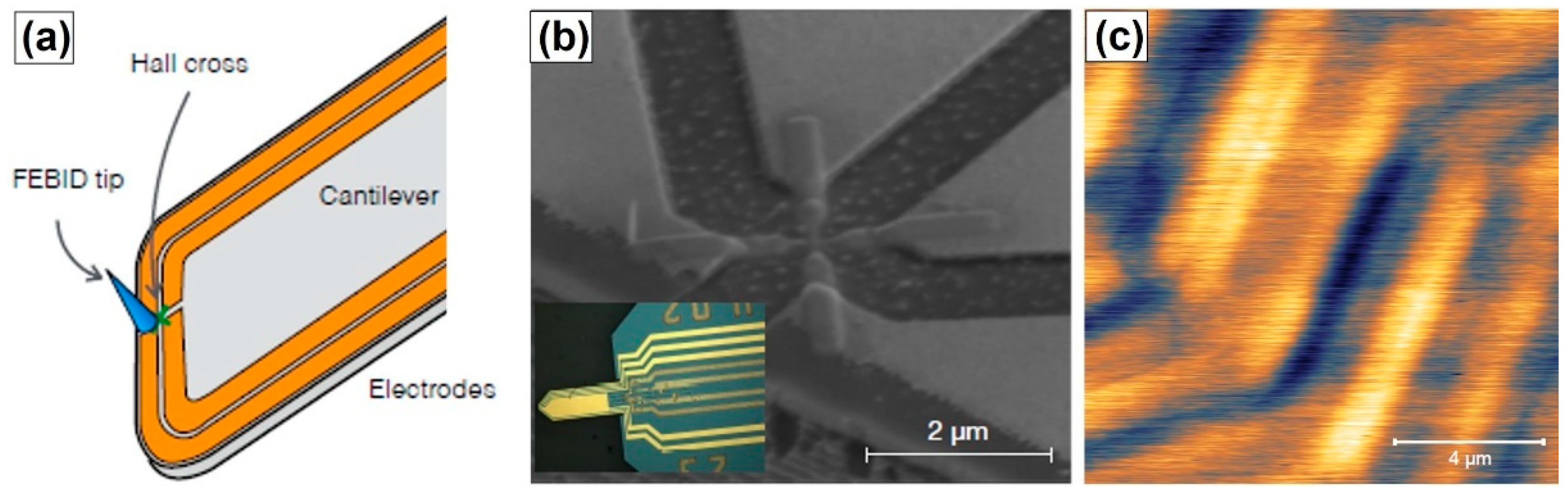
4. Scanning Ferromagnetic Hall Sensors
Scanning probe microscopy has recently spread its scope through the use of advanced ferromagnetic Hall sensors [73], underpinning their potential for stray field characterization of magnetic samples minimizing the invasiveness. Gabureac et al. explored the performance of Hall sensors fabricated with Co-FEBID, with a lateral size of 50 × 50 nm2, reaching a magnetic field sensitivity of 1 Ω·T−1 and a resolution of 1 μT·Hz−1/2, benefitting from the intergranular scattering of the microstructure [22]. Years later, FEBID granular ferromagnets were grown by M. Huth and co-workers to be used in scanning Hall probe microscopy, exhibiting an extremely high stray field sensitivity and a lateral resolution of 500 nm, limited due to the probe geometry [73]. As shown in Figure 10, the granular ferromagnet Hall sensors were grown in the insulating area located between the Cr/Au electrodes. This design allowed to acquire the first scanning Hall probe images of a magnetic tape where bits with different magnetization orientation can be seen with this type of sensor (see Figure 10c).
5. Magnetic Resonance Force Microscopy
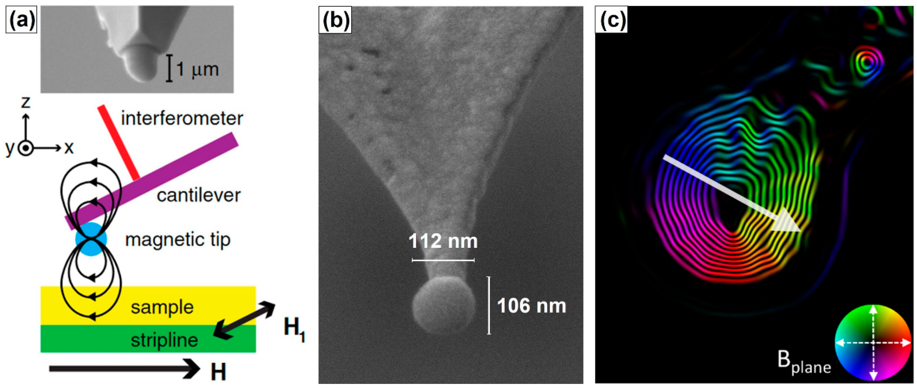
MRFM encompasses the interaction between tip and sample to unveil the spin dynamics properties of a magnetic sample [74,75]. This imaging technique allows for exploring the spatial distribution of magnetic resonance modes of nano-objects. It should be highlighted the study of permalloy disks measured with 100 nm magnetic lateral resolution for the detection of spin waves modes localized in the structure [37]. Similarly, as shown in Figure 11a, Chia et al. reported the fabrication of magnetic Co nanocube tips by FEBID used for the generation and detection of localized spin wave precession modes in thin films [76]. In this example, an external magnetic field aligns the tip and sample magnetization in the same plane. A microwave field , perpendicular to , drives the spin precession near the ferromagnetic resonance frequency, eventually producing a cantilever deflection. More recently, Sangiao et al. reported the use of magnetic FEBID Co nanospheres in magnetic vortex state, see Figure 11b,c, aiming at minimizing the hysteresis effects and favouring quantitative analyses of the MRFM signals optimized by the high magnetization values of the functionalized probe [77].
6. Conclusions
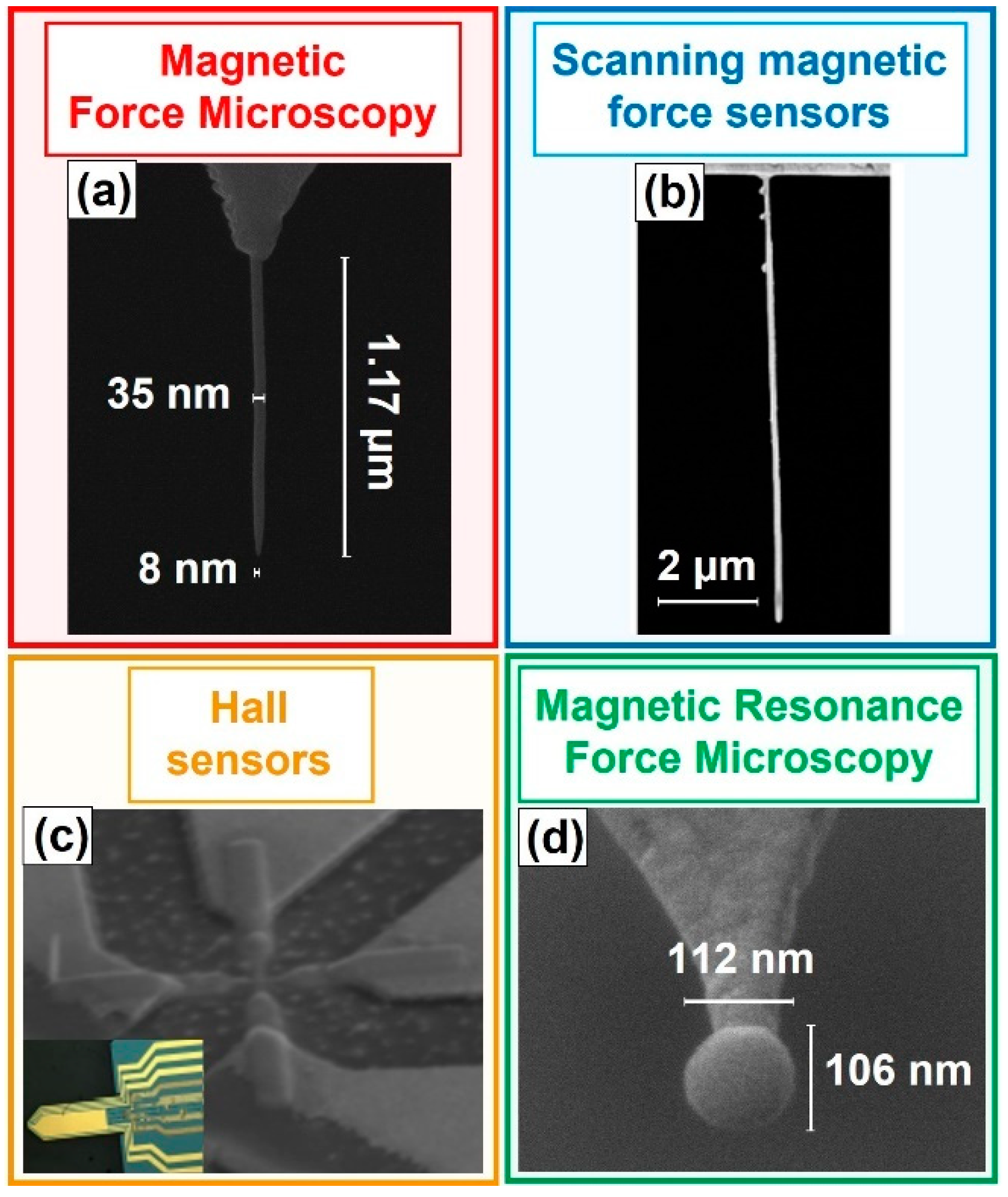
The versatility of FEBID for the functionalization of AFM cantilevers with magnetic nanostructures has been discussed. Particularly, the reproducible shape tunability enables the fabrication of 3D ferromagnets, i.e., nanowires, nanocubes, and nanospheres, with accurate positioning onto the probes, as shown for some selected sensing devices in Figure 12. The geometrical customization has opened new alternatives for different operational modes in MFM, MRFM, Magnetic Force Sensing and Scanning ferromagnetic Hall sensors, giving rise to magnetic sensors with high quality performance in terms of resolution, sensitivity, and mechanical stability.
The use of alternative nanostructured materials on the probes for distinct functionalities, especially feasible due to the broad range of available FEBID precursor gases, the growth of more complex geometries, thanks to the application of computer-aided design programs, and the implementation of post-growth approaches for further tunability of the composition, crystallinity, and magnetic properties of the structures have a great potential for the future. This upcoming research may contribute, for instance, to the development of quantitative MFM, where the retrieval of magnetic information requires tips with well- optimized and well-defined properties.
Author Contributions
Conceptualization, J.P.-N., S.S., C.M. and J.M.d.T.; investigation, J.P.-N., S.S., C.M. and J.M.d.T.; writing—original draft preparation, J.P.-N.; writing—review and editing, J.P.-N., S.S., C.M. and J.M.d.T. All authors have read and agreed to the published version of the manuscript.
Funding
This research was funded by the Spanish Ministry of Economy and Competitiveness through the projects PID2020-112914RB-100, MAT2017-82970-C2-1-R, MAT2017-82970-C2-2-R and MAT2018-102627-T, BES-2015-072950, the Aragon Regional Government (Construyendo Europa desde Aragón) through the project E13_20R with European Social Fund funding. This work has received funding from the European’s Union Horizon 2020 research and innovation programme under Grant No. 823717-ESTEEM3.
Data Availability Statement
The data presented in this study are available upon reasonable request from the corresponding author.
Acknowledgments
Experimental help and scientific discussions with A. Asenjo, M. Jaafar, M. Poggio and G. de Loubens are acknowledged.
Conflicts of Interest
The authors declare no conflict of interest.
References
- Matsui, S.; Mori, K. New Selective Deposition Technology by Electron Beam Induced Surface Reaction. Jpn. J. Appl. Phys. 1984, 23, L706. [Google Scholar] [CrossRef]
- Huth, M.; Porrati, F.; Schwalb, C.; Winhold, M.; Sachser, R.; Dukic, M.; Adams, J.; Fantner, G. Focused electron beam induced deposition: A perspective. Beilstein J. Nanotechnol. 2012, 3, 597–619. [Google Scholar] [CrossRef] [PubMed] [Green Version]
- Randolph, S.J.; Fowlkes, J.D.; Rack, P.D. Focused, Nanoscale Electron-Beam-Induced Deposition and Etching. Crit. Rev. Solid State Mater. Sci. 2006, 31, 55–89. [Google Scholar] [CrossRef]
- Van Dorp, W.F.; Hagen, C.W. A critical literature review of focused electron beam induced deposition. J. Appl. Phys. 2008, 104, 081301. [Google Scholar] [CrossRef] [Green Version]
- Utke, I.; Hoffmann, P.; Melngailis, J. Gas-assisted focused electron beam and ion beam processing and fabrication. J. Vac. Sci. Technol. 2008, 26, 1197. [Google Scholar] [CrossRef] [Green Version]
- Plank, H.; Smith, D.A.; Haber, T.; Rack, P.D.; Hofer, F. Fundamental Proximity Effects in Focused Electron Beam Induced Deposition. ACS Nano 2012, 6, 286–294. [Google Scholar] [CrossRef]
- Winkler, R.; Szkudlarek, A.; Fowlkes, J.D.; Rack, P.D.; Utke, I.; Plank, H. Toward Ultraflat Surface Morphologies During Focused Electron Beam Induced Nanosynthesis: Disruption Origins and Compensation. ACS Appl. Mater. Interfaces 2015, 7, 3289–3297. [Google Scholar] [CrossRef]
- Höflich, K.; Yanh, R.B.; Berger, A.; Leuchs, G.; Christiansen, S. The Direct Writing of Plasmonic Gold Nanostructures by Electron-Beam-Induced Deposition. Adv. Mater. 2011, 23, 2657–2661. [Google Scholar] [CrossRef]
- Mitsuishi, K.; Shimojo, M.; Tanaka, M.; Takeguchi, M.; Furuya, K. Resolution in New Nanofabrication Technique Combining Electron-Beam-Induced Deposition and Low-Energy Ion Milling. Jpn. J. Appl. Phys. 2005, 44, 5627. [Google Scholar] [CrossRef]
- Fedorov, A.G.; Kim, S.; Henry, M.; Kulkarni, D.; Tsukruk, V.V. Focused-electron-beam-induced processing (FEBIP) for emerging applications in carbon nanoelectronics. Appl. Phys. A 2014, 117, 1659–1674. [Google Scholar] [CrossRef]
- Serrano-Ramón, L.; Córdoba, R.; Rodríguez, L.A.; Magén, C.; Snoeck, E.; Gatel, C.; Serrano, I.; Ibarra, M.R.; de Teresa, J.M. Ultrasmall functional ferromagnetic nanostructures grown by focused electron-beam-induced deposition. ACS Nano 2011, 5, 7781–7787. [Google Scholar] [CrossRef] [Green Version]
- De Teresa, J.M.; Córdoba, R. Arrays of Densely Packed Isolated Nanowires by Focused Beam Induced Deposition Plus Ar+ Milling. ACS Nano 2014, 8, 3788–3795. [Google Scholar] [CrossRef] [PubMed]
- Boero, G.; Utke, I.; Bret, T.; Quack, N.; Todorova, M.; Mouaziz, S.; Kejik, P.; Brugger, J.; Popovic, R.S.; Hoffmann, P. Submicrometer Hall devices fabricated by focused electron-beam-induced deposition. Appl. Phys. Lett. 2005, 86, 042503. [Google Scholar] [CrossRef] [Green Version]
- Fernández-Pacheco, A.; Serrano-Ramón, L.; Michalik, J.M.; Ibarra, M.R.; de Teresa, J.M.; O’Brien, L.; Petit, D.; Lee, J.; Cowburn, R.P. Three dimensional magnetic nanowires grown by focused electron-beam induced deposition. Sci. Rep. 2013, 3, 1492. [Google Scholar] [CrossRef] [PubMed] [Green Version]
- Van Kouwen, L.; Botman, A.; Hagen, C.W. Focused Electron-Beam-Induced Deposition of 3 nm Dots in a Scanning Electron Microscope. Nano Lett. 2009, 9, 2149–2152. [Google Scholar] [CrossRef] [PubMed]
- Gavagnin, M.; Wanzenboeck, H.D.; Belić, D.; Bertagnolli, E. Synthesis of Individually Tuned Nanomagnets for Nanomagnet Logic by Direct Write Focused Electron Beam Induced Deposition. ACS Nano 2013, 7, 777–784. [Google Scholar] [CrossRef]
- Skoric, L.; Sanz-Hernández, D.; Meng, F.; Donnelly, C.; Merino-Aceituno, S.; Fernández-Pacheco, A. Layer-by-Layer Growth of Complex-Shaped Three-Dimensional Nanostructures with Focused Electron Beams. Nano Lett. 2020, 20, 184–191. [Google Scholar] [CrossRef]
- Winkler, R.; Fowlkes, J.D.; Rack, P.D.; Kothleitner, G.; Plank, H. Shape evolution and growth mechanisms of 3D-printed nanowires. Addit. Manuf. 2021, 46, 102076. [Google Scholar]
- Riazanova, A.V.; Costanzi, B.N.; Aristov, A.; Rikers, Y.G.M.; Ström, V.; Mulders, J.J.L.; Kabashin, A.V.; Dahlberg, E.D.; Belova, L.M. Gas-assisted electron-beam-induced nanopatterning of high-quality Si-based insulator. Nanotechnology 2014, 25, 155301. [Google Scholar] [CrossRef]
- Sengupta, S.; Li, C.; Baumier, C.; Kasumov, A.; Guéron, S.; Bouchiat, H.; Fortuna, F. Superconducting nanowires by electron-beam-induced deposition. Appl. Phys. Lett. 2015, 106, 042601. [Google Scholar] [CrossRef] [Green Version]
- Utke, I.; Hoffmann, P.; Berger, R.; Scandella, L. High-resolution magnetic Co supertips grown by a focused electron beam. Appl. Phys. Lett. 2002, 80, 4792. [Google Scholar] [CrossRef]
- Gabureac, M.; Bernau, L.; Utke, I.; Boero, G. Granular Co-C nano-Hall sensors by focused-beam-induced deposition. Nanotechnology 2010, 21, 115503. [Google Scholar] [CrossRef] [PubMed] [Green Version]
- Graells, S.; Aćimović, S.; Volpe, G.; Quidant, R. Direct Growth of Optical Antennas Using E-Beam-Induced Gold Deposition. Plasmonics 2010, 5, 135–139. [Google Scholar] [CrossRef]
- Fernández-Pacheco, A.; de Teresa, J.M.; Córdoba, R.; Ibarra, M.R. Magnetotransport properties of high-quality cobalt nanowires grown by focused-electron-beam-induced deposition. J. Phys. D Appl. Phys. 2009, 42, 055005. [Google Scholar] [CrossRef] [Green Version]
- Takeguchi, M.; Shimojo, M.; Furuya, K. Fabrication of magnetic nanostructures using electron beam induced chemical vapour deposition. Nanotechnology 2005, 16, 1321. [Google Scholar] [CrossRef]
- Lavrijsen, R.; Córdoba, R.; Schoenaker, F.J.; Ellis, T.H.; Barcones, B.; Kohlhepp, J.T.; Swagten, H.J.M.; Koopmans, B.; de Teresa, J.M.; Magén, C.; et al. Fe:O:C grown by focused-electron-beam-induced deposition: Magnetic and electric properties. Nanotechnology 2010, 22, 025302. [Google Scholar] [CrossRef] [PubMed] [Green Version]
- Parentes, A.; Sinicco, G.; Boero, G.; Dwir, B.; Hoffmann, P. Focused electron beam induced deposition of nickel. J. Vac. Sci. Technol. 2007, 25, 2228. [Google Scholar] [CrossRef]
- Córdoba, R.; Barcones, B.; Roelfsema, E.; Verheijen, M.A.; Mulders, J.J.L.; Trompenaars, P.H.F.; Koopmans, B. Functional nickel-based deposits synthesized by focused beam induced processing. Nanotechnology 2016, 27, 065303. [Google Scholar] [CrossRef]
- Nikulina, E.; Idigoras, O.; Porro, J.M.; Vavassori, P.; Chuvilin, A.; Berger, A. Origin and control of magnetic exchange coupling in between focused electron beam deposited cobalt nanostructures. Appl. Phys. Lett. 2013, 103, 123112. [Google Scholar] [CrossRef]
- Gavagnin, M.; Wanzenboeck, H.D.; Belic, D.; Shawrav, M.M.; Persson, A.; Gunnarsson, K.; Svedlindh, P.; Bertagnolli, E. Magnetic force microscopy study of shape engineered FEBID iron nanostructures. Phys. Status Solidi A 2014, 211, 368–374. [Google Scholar] [CrossRef]
- Fernández-Pacheco, A.; de Teresa, J.M. Present and future applications of magnetic nanostructures grown by FEBID. Appl. Phys. A 2014, 117, 1645–1658. [Google Scholar]
- De Teresa, J.M.; Fernández-Pacheco, A.; Córdoba, R.; Serrano-Ramón, L.; Sangiao, S.; Ibarra, M.R. Review of magnetic nanostructures grown by focused electron beam induced deposition (FEBID). J. Phys. D Appl. Phys. 2016, 49, 243003. [Google Scholar] [CrossRef]
- Fernández-Pacheco, A.; Skoric, L.; de Teresa, J.M.; Pablo-Navarro, J.; Huth, M.; Dobrovolskiy, O.V. Writing 3D Nanomagnets Using Focused Electron Beams. Materials 2020, 13, 3774. [Google Scholar] [CrossRef] [PubMed]
- Meng, F.; Donnelly, C.; Skoric, L.; Hierro-Rodriguez, A.; Liao, J.-W.; Fernández-Pacheco, A. Fabrication of a 3D Nanomagnetic Circuit with Multi-Layered Materials for Applications in Spintronics. Micromachines 2021, 12, 859. [Google Scholar] [CrossRef] [PubMed]
- Magén, C.; Pablo-Navarro, J.; de Teresa, J.M. Focused-Electron-Beam Engineering of 3D Magnetic Nanowires. Nanomaterials 2021, 11, 402. [Google Scholar] [CrossRef] [PubMed]
- Gavagnin, M.; Wanzenboeck, H.D.; Wachter, S.; Shawrav, M.M.; Persson, A.; Gunnarsson, K.; Svedlindh, P.; Stöger-Pollach, M.; Bertagnolli, E. Free-Standing Magnetic Nanopillars for 3D Nanomagnet Logic. ACS Appl. Mater. Interfaces 2014, 6, 20254–20260. [Google Scholar] [CrossRef] [PubMed]
- Guo, F.; Belova, L.M.; McMichael, R.D. Spectroscopy and Imaging of Edge Modes in Permalloy Nanodisks. Phys. Rev. Lett. 2013, 110, 017601. [Google Scholar] [CrossRef] [PubMed] [Green Version]
- Sharma, N.; van Mourik, R.A.; Yin, Y.; Koopmans, B.; Parkin, S.S.P. Focused-electron-beam-induced-deposited cobalt nanopillars for nanomagnetic logic. Nanotechnology 2016, 27, 165301. [Google Scholar] [CrossRef] [PubMed]
- Dobrovolskiy, O.V.; Begun, E.; Huth, M.; Shklovskij, V.A.; Tsindlekht, M.I. Vortex lattice matching effects in a washboard pinning potential induced by Co nanostripe arrays. Phys. C Supercond. Appl. 2011, 471, 449–452. [Google Scholar] [CrossRef]
- Vavassori, P.; Pancaldi, M.; Perez-Roldan, M.J.; Chuvilin, A.; Berger, A. Remote Magnetomechanical Nanoactuation. Small 2016, 12, 1013–1023. [Google Scholar] [CrossRef] [PubMed]
- Jaafar, M.; Pablo-Navarro, J.; Berganza, E.; Ares, P.; Magén, C.; Masseboeuf, A.; Gatel, C.; Snoeck, E.; Gómez-Herrero, J.; de Teresa, J.M.; et al. Customized MFM probes based on magnetic nanorods. Nanoscale 2020, 12, 10090–10097. [Google Scholar] [CrossRef] [PubMed]
- Berganza, E.; Jaafar, M.; Fernandez-Roldan, J.A.; Goiriena-Goikoetxea, M.; Pablo-Navarro, J.; García-Arribas, A.; Guslienko, K.; Magén, C.; de Teresa, J.M.; Chubykalo-Fesenko, O.; et al. Half-hedgehog spin textures in sub-100 nm soft magnetic nanodots. Nanoscale 2020, 12, 18646–18653. [Google Scholar] [CrossRef]
- Mattiat, H.; Rossi, N.; Gross, B.; Pablo-Navarro, J.; Magén, C.; Badea, R.; Berezovsky, J.; de Teresa, J.M.; Poggio, M. Nanowire Magnetic Force Sensors Fabricated by Focused-Electron-Beam-Induced Deposition. Phys. Rev. Appl. 2020, 13, 044043. [Google Scholar] [CrossRef] [Green Version]
- Rossi, N.; Gross, B.; Dirnberger, F.; Bougeard, D.; Poggio, M. Magnetic Force Sensing Using a Self-Assembled Nanowire. Nano Lett. 2019, 19, 930–936. [Google Scholar] [CrossRef] [PubMed]
- Sidles, J.A.; Garbini, J.L.; Bruland, K.J.; Rugar, D.; Züger, O.; Hoen, S.; Yannoni, C.S. Magnetic resonance force microscopy. Rev. Mod. Phys. 1995, 67, 249. [Google Scholar] [CrossRef]
- Kazakova, O.; Puttock, R.; Barton, C.; Corte-León, H.; Jaafar, M.; Neu, V.; Asenjo, A. Frontiers of magnetic force microscopy. J. Appl. Phys. 2019, 125, 060901. [Google Scholar] [CrossRef]
- Ares, P.; Jaafar, M.; Gil, A.; Gómez-Herrero, J.; Asenjo, A. Magnetic Force Microscopy in Liquids. Small 2015, 11, 4731–4736. [Google Scholar] [CrossRef] [PubMed] [Green Version]
- Belova, L.M.; Hellwig, O.; Dobisz, E.; Dahlberg, E.D. Rapid preparation of electron beam induced deposition Co magnetic force microscopy tips with 10 nm spatial resolution. Rev. Sci. Instrum. 2012, 83, 093711. [Google Scholar] [CrossRef]
- Koblischka, M.R.; Hartmann, U.; Sulzbach, T. Improving the lateral resolution of the MFM technique to the 10 nm range. J. Magn. Magn. Mater. 2004, 272–276, 2138–2140. [Google Scholar] [CrossRef]
- Iglesias-Freire, Ó.; Jaafar, M.; Berganza, E.; Asenjo, A. Customized MFM probes with high lateral resolution. Beilstein J. Nanotechnol. 2016, 7, 1068–1074. [Google Scholar] [CrossRef] [PubMed] [Green Version]
- Román García, E.L.; Martínez-Orellana, L.; Díaz Lagos, M.; Huttel, Y. Modification of Atomic Force Microscopy Tips by Deposition of Nanoparticles with an Aggregate Source. Patent WO/2011/141602, 4 May 2011. [Google Scholar]
- Amos, N.; Ikkawi, R.; Haddon, R.; Litvinov, D.; Khizroev, S. Controlling multidomain states to enable sub-10-nm magnetic force microscopy. Appl. Phys. Lett. 2008, 93, 203116. [Google Scholar] [CrossRef]
- Kuramochi, H.; Uzumaki, T.; Yasutake, M.; Tanaka, A.; Akinaga, H.; Yokoyama, H. A magnetic force microscope using CoFe-coated carbon nanotube probes. Nanotechnology 2004, 16, 24. [Google Scholar] [CrossRef]
- Yang, C.; Tang, J.; Kato, S.; Zhang, Q.; Qin, L.C.; Woodson, M.; Liu, J.; Kim, J.W.; Littlehei, P.T.; Park, C.; et al. Magnetic nanowire based high resolution magnetic force microscope probes. Appl. Phys. Lett. 2005, 87, 123507. [Google Scholar] [CrossRef]
- Campanella, H.; Jaafar, M.; Llobet, J.; Esteve, J.; Vázquez, M.; Asenjo, A.; del Real, R.P.; Plaza, J.A. Nanomagnets with high shape anisotropy and strong crystalline anisotropy: Perspectives on magnetic force microscopy. Nanotechnology 2011, 22, 505301. [Google Scholar] [CrossRef] [PubMed]
- Lau, Y.M.; Chee, P.C.; Thong, J.T.L.; Ng, V. Properties and applications of cobalt-based material produced by electron-beam-induced deposition. J. Vac. Sci. Technol. A 2002, 20, 1295. [Google Scholar] [CrossRef] [Green Version]
- Alotaibi, S.; Samba, J.; Pokharel, S.; Lan, Y.; Uradu, K.; Afolabi, A.; Unlu, I.; Basnet, G.; Aslan, K.; Flanders, B.N.; et al. Individually grown cobalt nanowires as magnetic force microscopy probes. Appl. Phys. Lett. 2018, 112, 092401. [Google Scholar] [CrossRef] [PubMed]
- Stiller, M.; Barzola-Quiquia, J.; Esquinazi, P.D.; Sangiao, S.; de Teresa, J.M.; Meijer, J.; Abel, B. Functionalized Akiyama tips for magnetic force microscopy measurements. Meas. Sci. Technol. 2017, 28, 125401. [Google Scholar] [CrossRef] [Green Version]
- Plank, H.; Winkler, R.; Schwalb, C.H.; Hütner, J.; Fowlkes, J.D.; Rack, P.D.; Utke, I.; Huth, M. Focused Electron Beam-Based 3D Nanoprinting for Scanning Probe Microscopy: A Review. Micromachines 2020, 11, 48. [Google Scholar] [CrossRef] [PubMed] [Green Version]
- Toth, M.; Lobo, C.; Friedli, V.; Szkudlarek, A.; Utke, I. Continuum models of focused electron beam induced processing. Beilstein J. Nanotechnol. 2015, 6, 1518–1540. [Google Scholar] [CrossRef] [PubMed]
- Pablo-Navarro, J. Development and Optimization of 3D Advanced Functional Magnetic Nanostructures Grown by Focused Electron Beam Induced Deposition. Ph.D. Thesis, University of Zaragoza, Zaragoza, Spain, 2020. [Google Scholar]
- Pablo-Navarro, J.; Magén, C.; de Teresa, J.M. Three-dimensional core-shell ferromagnetic nanowires grown by focused electron beam induced deposition. Nanotechnology 2016, 27, 285302. [Google Scholar] [CrossRef]
- Pablo-Navarro, J.; Sanz-Hernández, D.; Magén, C.; Fernández-Pacheco, A.; de Teresa, J.M. Tuning shape, composition and magnetization of 3D cobalt nanowires grown by focused electron beam induced deposition (FEBID). J. Phys. D Appl. Phys. 2017, 50, 18LT01. [Google Scholar] [CrossRef]
- Córdoba, R.; Sesé, J.; de Teresa, J.M.; Ibarra, M.R. High-purity cobalt nanostructures grown by focused-electron-beam-induced deposition at low current. Microelectron. Eng. 2010, 87, 1550–1553. [Google Scholar] [CrossRef]
- Bernau, L.; Gabureac, M.; Erni, R.; Utke, I. Tunable Nanosynthesis of Composite Materials by Electron-Impact Reaction. Angew. Chem. 2010, 122, 9064–9068. [Google Scholar] [CrossRef]
- Pablo-Navarro, J.; Winkler, R.; Haberfehlner, G.; Magén, C.; Plank, H.; de Teresa, J.M. In situ real-time annealing of ultrathin vertical Fe nanowires grown by focused electron beam induced deposition. Acta Mater. 2019, 174, 379–386. [Google Scholar] [CrossRef]
- Shimojo, M.; Takeguchi, M.; Tanaka, M.; Mitsuishi, K.; Furuya, K. Electron beam-induced deposition using iron carbonyl and the effects of heat treatment on nanostructure. Appl. Phys. A 2004, 79, 1869–1872. [Google Scholar] [CrossRef]
- Nečas, D.; Klapetek, P.; Neu, V.; Havlíček, M.; Puttock, R.; Kazakova, O.; Hu, X.; Zajíčková, L. Determination of tip transfer function for quantitative MFM using frequency domain filtering and least squares method. Sci. Rep. 2019, 9, 3880. [Google Scholar] [CrossRef]
- Rack, P.D.; Fowlkes, J.D.; Randolph, S.J. In situ probing of the growth and morphology in electron-beam-induced deposited nanostructures. Nanotechnology 2007, 18, 465602. [Google Scholar] [CrossRef] [PubMed]
- AsdWolf, D.; Rodriguez, L.A.; Béché, A.; Javon, E.; Serrano, L.; Magen, C.; Gatel, C.; Lubk, A.; Lichte, H.; Bals, S.; et al. 3D Magnetic Induction Maps of Nanoscale Materials Revealed by Electron Holographic Tomography. Chem. Mater. 2015, 27, 6771–6778. [Google Scholar]
- Wang, C.; Xiao, D.; Chen, X.; Zhou, Y.; Liu, Y. Manipulating and trapping skyrmions by magnetic field gradients. New J. Phys. 2017, 19, 083008. [Google Scholar] [CrossRef] [Green Version]
- García, R.; Pérez, R. Dynamic atomic force microscopy methods. Surf. Sci. Rep. 2002, 47, 197–301. [Google Scholar] [CrossRef]
- Sachser, R.; Hütner, J.; Schwalb, C.H.; Huth, M. Granular Hall Sensors for Scanning Probe Microscopy. Nanomaterials 2021, 11, 348. [Google Scholar] [CrossRef] [PubMed]
- Zhang, Z.; Hammel, P.C.; Wigen, P.E. Observation of ferromagnetic resonance in a microscopic sample using magnetic resonance force microscopy. Appl. Phys. Lett. 1996, 68, 2005. [Google Scholar] [CrossRef] [Green Version]
- Klein, O.; de Loubens, G.; Naletov, V.V.; Boust, F.; Guillet, T.; Hurdequint, H.; Leksikov, A.; Slavin, A.N.; Tiberkevich, V.S.; Vukadinovic, N. Ferromagnetic resonance force spectroscopy of individual submicron-size samples. Phys. Rev. B 2008, 78, 144410. [Google Scholar] [CrossRef] [Green Version]
- Chia, H.-J.; Guo, F.; Belova, L.M.; McMichael, R.D. Nanoscale Spin Wave Localization Using Ferromagnetic Resonance Force Microscopy. Phys. Rev. Lett. 2012, 108, 087206. [Google Scholar] [CrossRef] [PubMed] [Green Version]
- Sangiao, S.; Magén, C.; Mofakhami, D.; de Loubens, G.; de Teresa, J.M. Magnetic properties of optimized cobalt nanospheres grown by focused electron beam induced deposition (FEBID) on cantilever tips. Beilstein J. Nanotechnol. 2017, 8, 2106–2115. [Google Scholar] [CrossRef] [PubMed]
Figure 1.
SEM images of (a) Nanoworld ArrowTM EFM, (b) Budget Sensors® and (c) Olympus BioLever mini AFM probes, with their corresponding (d,f) Fe and (e) Co nanowires. (a–c,f) adapted from [61] and (d,e) reproduced from [41] with permission from the Royal Society of Chemistry.

Figure 2.
MFM imaging of a high-density hard disk with (a) Budget Sensors Multi-M tip with 50 nm of CoCr coating, (b) Co-FEBID tip and (c) Fe-FEBID tip. (d–f) Topographic images obtained by the selected MFM probes and (g–i) their corresponding magnetic images, respectively. Reproduced from [41] with permission from the Royal Society of Chemistry.

Figure 3.
SEM images of (a) a core-shell Fe@Pt nanowire with a core diameter of 54 nm grown at 5 kV, (b) the thinnest 3D Fe nanowire ever achieved by us, grown at 30 kV, and (c) an Fe nanowire fabricated with an extremely sharp tip end with only ~8 nm in diameter grown at 30 kV, reproduced from [61]. (d) Study of the tip end morphology as a function of the voltage, adapted from [59].

Figure 4.
(a) Longitudinal chemical profile of an Fe nanowire grown on top of an AFM probe, obtained by STEM-EELS. The vertical short dash dot line represents the nanowire apex. (b) Representation of the magnetic flux lines illustrating the stray field distribution, obtained experimentally by electron holography, including insets with the TEM image (bottom), and the chemical map showing the relative composition of Fe, C, and O contents in green, blue, and red, respectively (top). Adapted from [61] and reproduced from [41] with permission from the Royal Society of Chemistry.

Figure 5.
MFM contrast, related to the stray field values, as a function of the magnetic tip section, and their corresponding MFM images of a standard commercial MFM probe (red), a tip with an Fe-FEBID nanowire with a blunt tip end of 50 nm (green), and with a sharp end of 7 nm (purple). Adapted from [61] and reproduced from [41] with permission from the Royal Society of Chemistry.

Figure 6.
Calculation of the magnetization as a function of the distance to the apex along the nanowire longitudinal axis direction for different (a) diameter, (b) length, and (c) values in the central region of the nanostructure. The QuickField software package was used. Reproduced from [61].
Figure 6.
Calculation of the magnetization as a function of the distance to the apex along the nanowire longitudinal axis direction for different (a) diameter, (b) length, and (c) values in the central region of the nanostructure. The QuickField software package was used. Reproduced from [61].

Figure 7.
MFM images of permalloy nanodots as a function of the in-plane magnetic field, obtained with a commercial magnetic tip by NanosensorsTM, a sputtered Co-coated tip and an Fe-FEBID nanowire tip. All image sizes are 250 250 nm2. Reproduced from [42] with permission from the Royal Society of Chemistry.

Figure 8.
Comparison of the MFM images of a hard disk acquired in air and water environments for the commercial NanosensorsTM PP-MFMR and Team Nanotec tips, and for the functionalized Olympus BioLever mini with an Fe-FEBID nanowire. Adapted from [61] and reproduced from [41] with permission from the Royal Society of Chemistry.

Figure 9.
(a) SEM image of a Co-FEBID nanowire. (b) Sketch of the nanowire flexural modes. (c) Projection of the flexural modes onto the X-Y plane. (d) Illustration of the detection scheme for the nanowire motion. (e) Thermally excited response of the upper and lower modes at room temperature. Adapted from [43].

Figure 10.
(a) Sketch of the self-sensing cantilever composed by the FEBID granular ferromagnetic Hall sensor cross surrounded by the Cr/Au electrodes. The non-magnetic FEBID tip was fabricated by Pt-C and is used for topographic information as an AFM tip. (b) SEM image of the granular ferromagnet Hall cross with the optical microscope image of the cantilever in the inset. (c) Scanning Hall probe microscopy image acquired with the granular ferromagnetic Hall sensor at 70 μA as the AC reference current. Adapted from [73].

Figure 11.
SEM images of (a) a 1.1 μm edge Co FEBID nanocube and (b) a 100 nm in diameter Co FEBID nanosphere used for MRFM. A sketch of the setup is illustrated in (a). (c) Magnetic induction flux map of the magnetic vortex state of the nanosphere. The inset shows the colour scale of the magnetic induction orientation. Adapted from [76,77].


Publisher’s Note: MDPI stays neutral with regard to jurisdictional claims in published maps and institutional affiliations. |
© 2021 by the authors. Licensee MDPI, Basel, Switzerland. This article is an open access article distributed under the terms and conditions of the Creative Commons Attribution (CC BY) license (https://creativecommons.org/licenses/by/4.0/).
Share and Cite
MDPI and ACS Style
Pablo-Navarro, J.; Sangiao, S.; Magén, C.; de Teresa, J.M. Magnetic Functionalization of Scanning Probes by Focused Electron Beam Induced Deposition Technology. Magnetochemistry 2021, 7, 140. https://doi.org/10.3390/magnetochemistry7100140
AMA Style
Pablo-Navarro J, Sangiao S, Magén C, de Teresa JM. Magnetic Functionalization of Scanning Probes by Focused Electron Beam Induced Deposition Technology. Magnetochemistry. 2021; 7(10):140. https://doi.org/10.3390/magnetochemistry7100140
Chicago/Turabian StylePablo-Navarro, Javier, Soraya Sangiao, César Magén, and José María de Teresa. 2021. "Magnetic Functionalization of Scanning Probes by Focused Electron Beam Induced Deposition Technology" Magnetochemistry 7, no. 10: 140. https://doi.org/10.3390/magnetochemistry7100140
Note that from the first issue of 2016, this journal uses article numbers instead of page numbers. See further details here.