
Simulation and Modeling of Novel Electronic Device Architectures with NESS (Nano-Electronic Simulation Software): A Modular Nano TCAD Simulation Framework

 , ,
, ,  , , , and
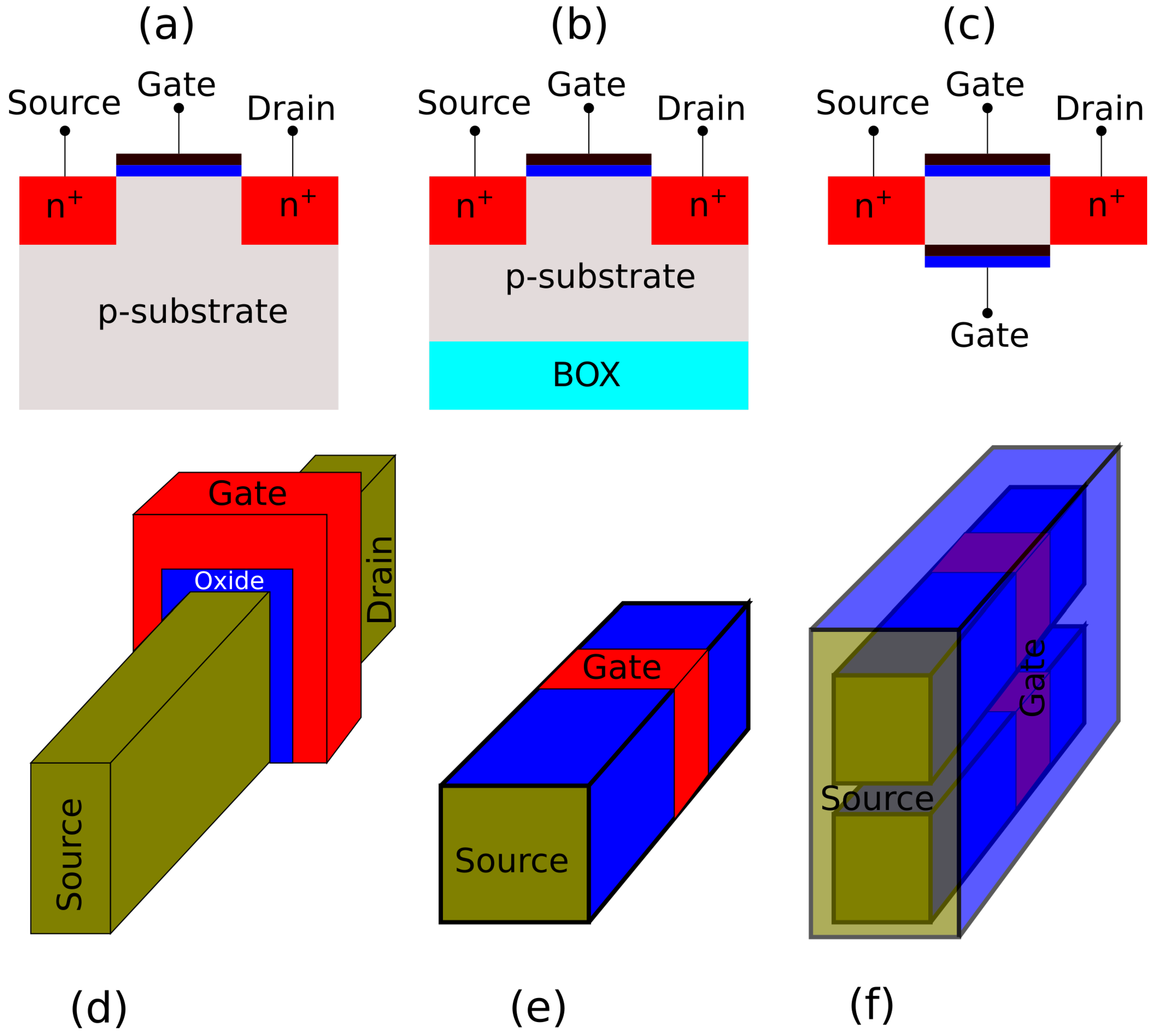
Abstract
:1. Introduction and State-of-the-Art
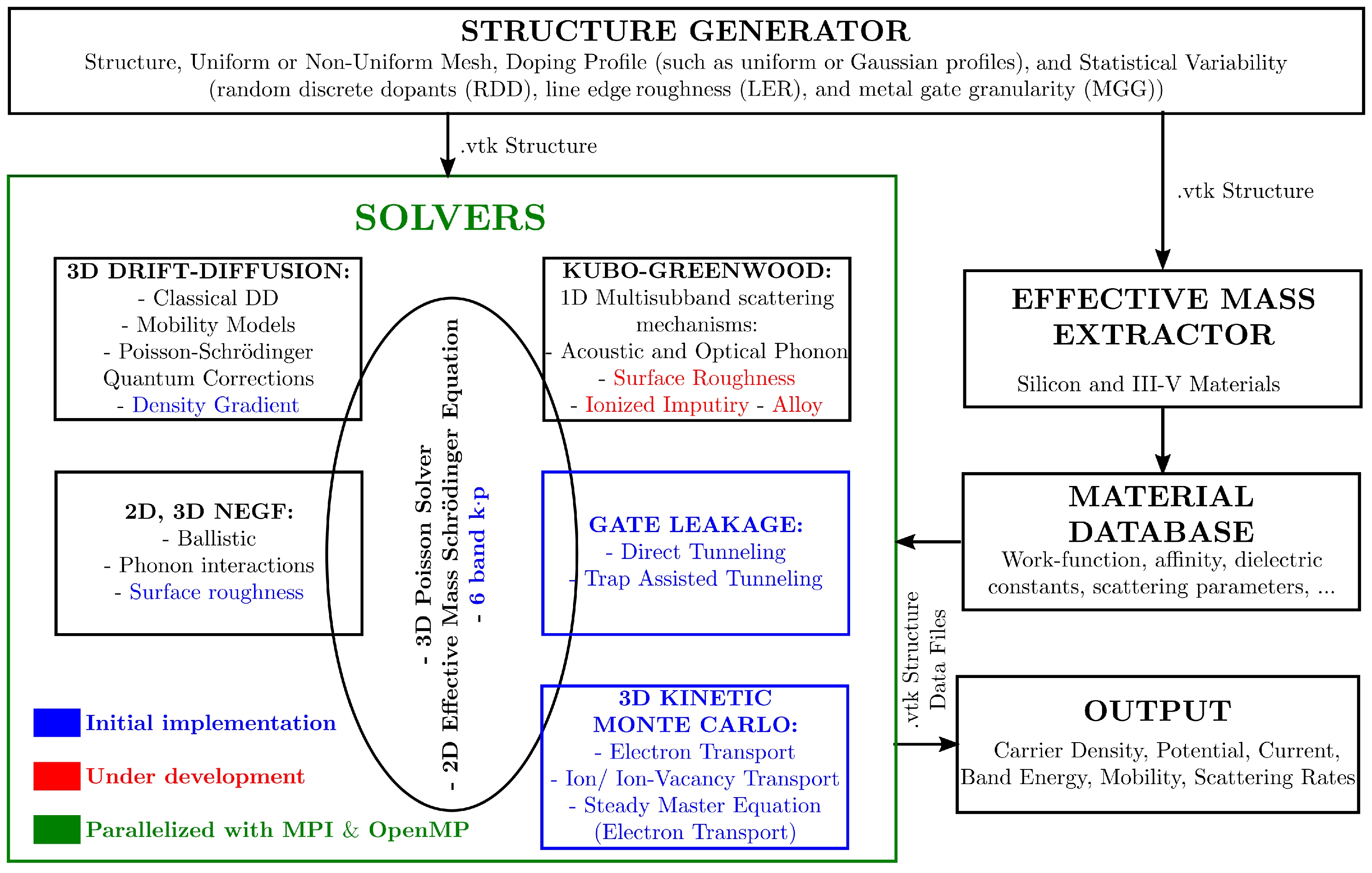
2. Overview of NESS
3. Non-Conventional or Future Devices
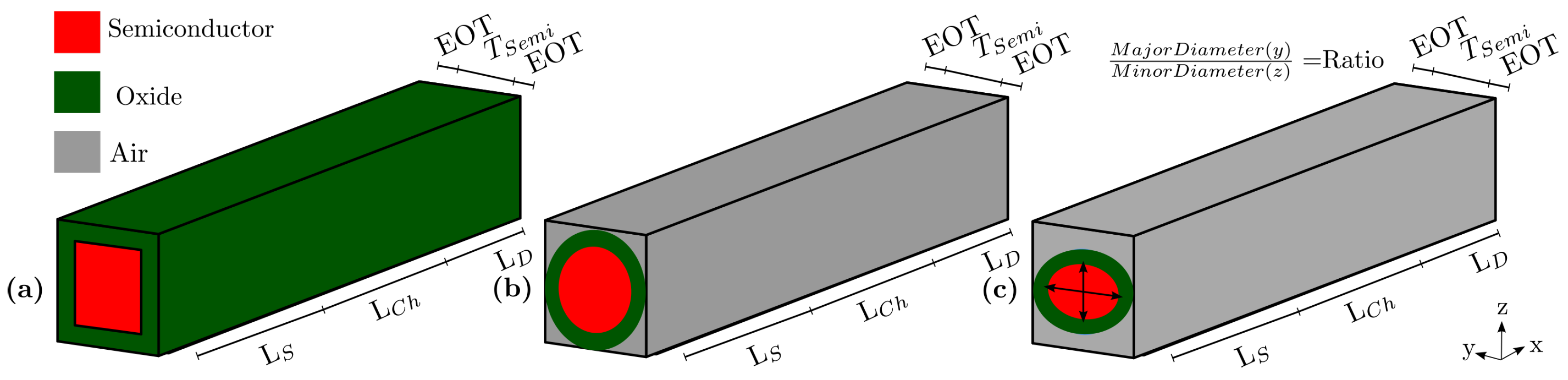
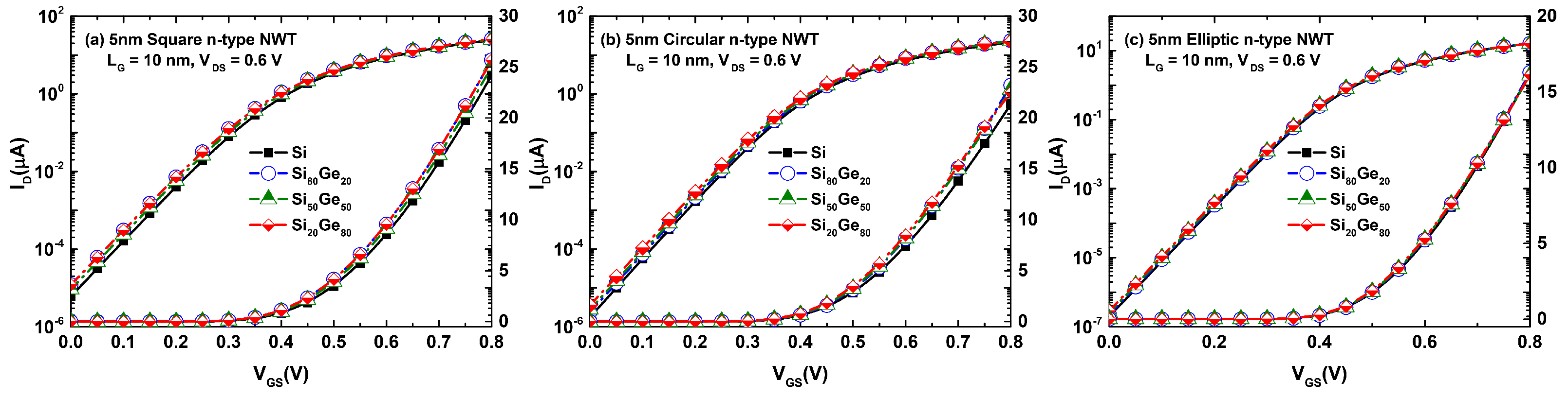
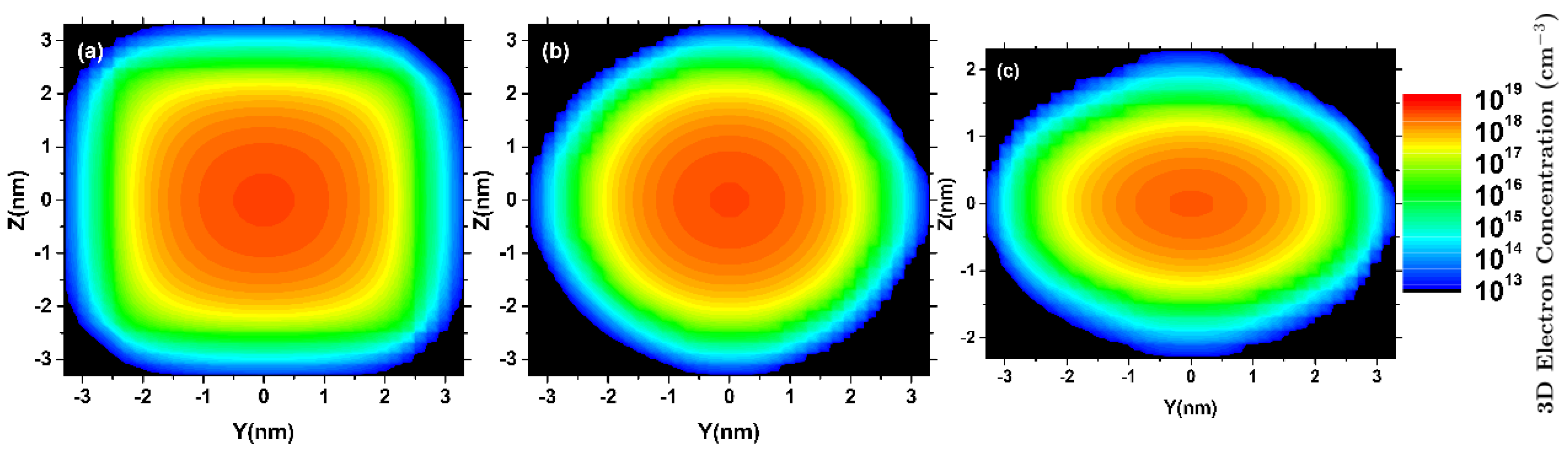
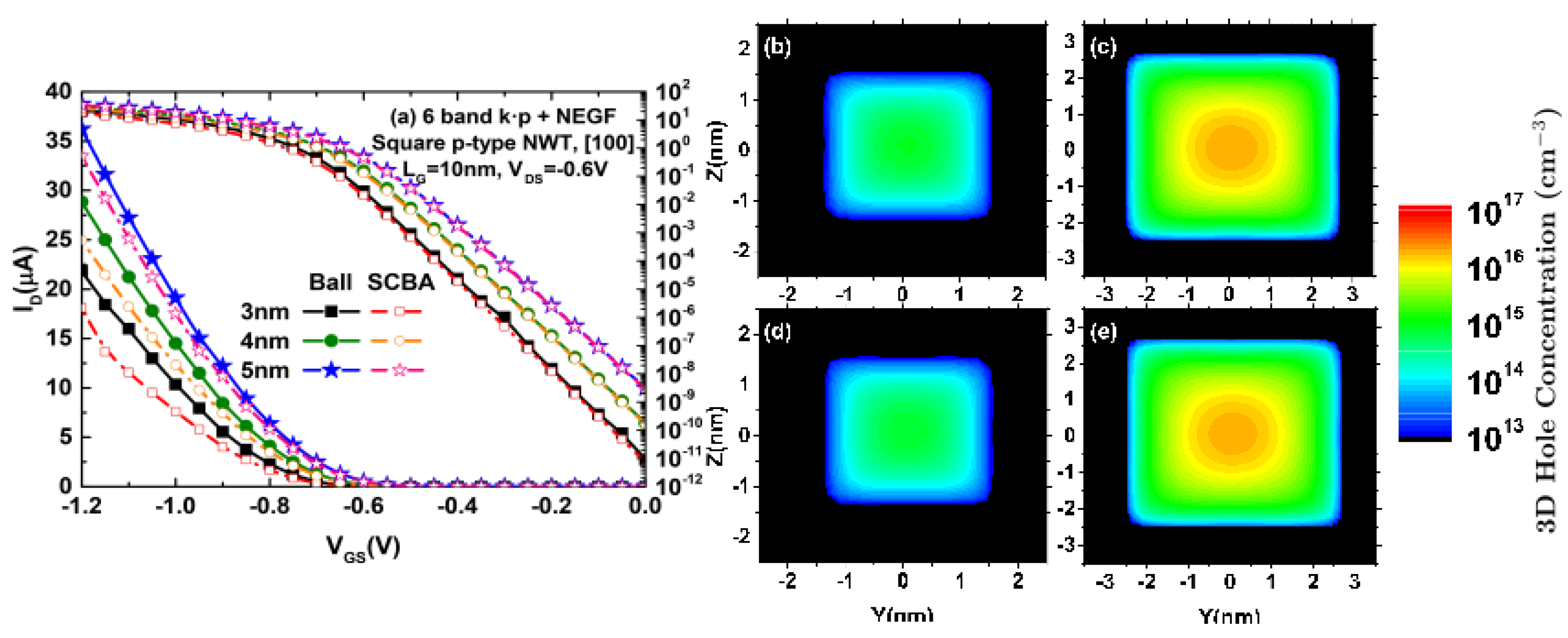
3.1. Nanowire Transistors
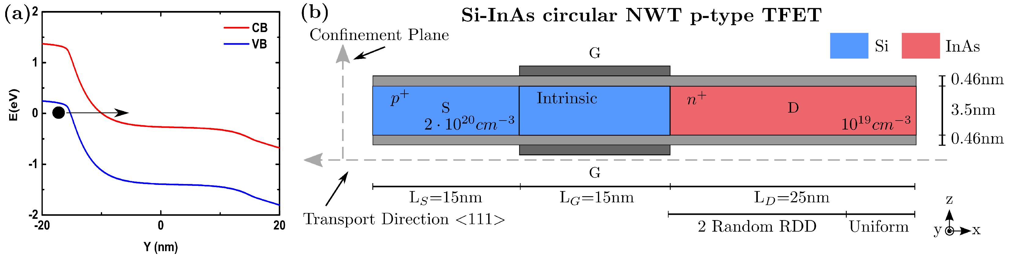
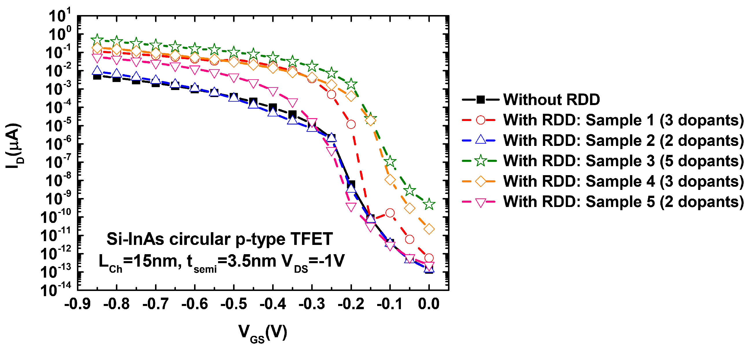
3.2. Tunnel FETs (TFET)
3.3. Negative Capacitance FETs (NCFET)
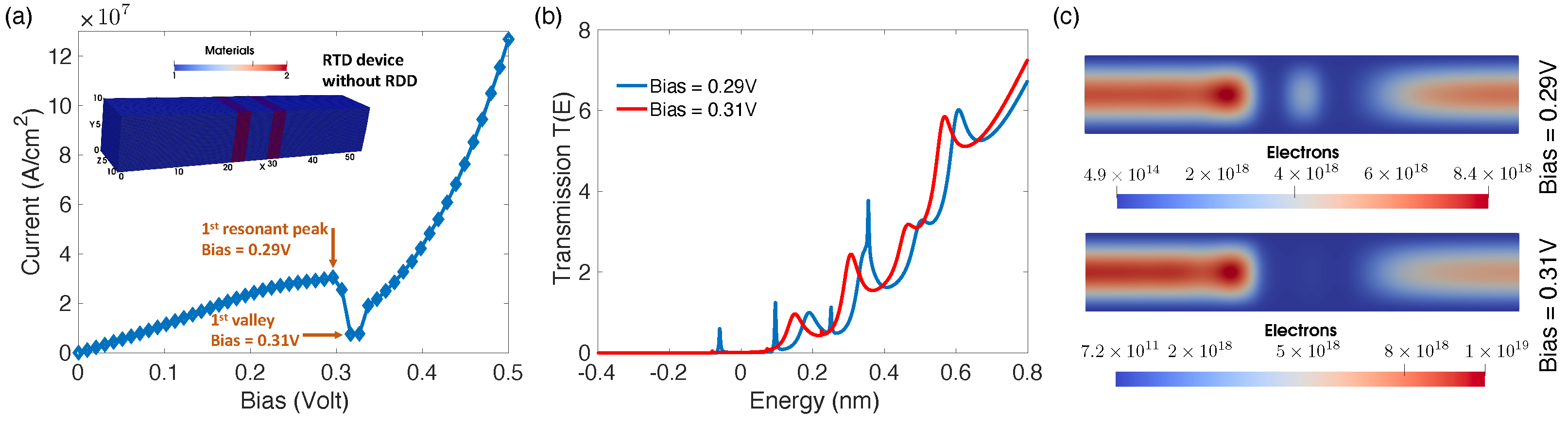
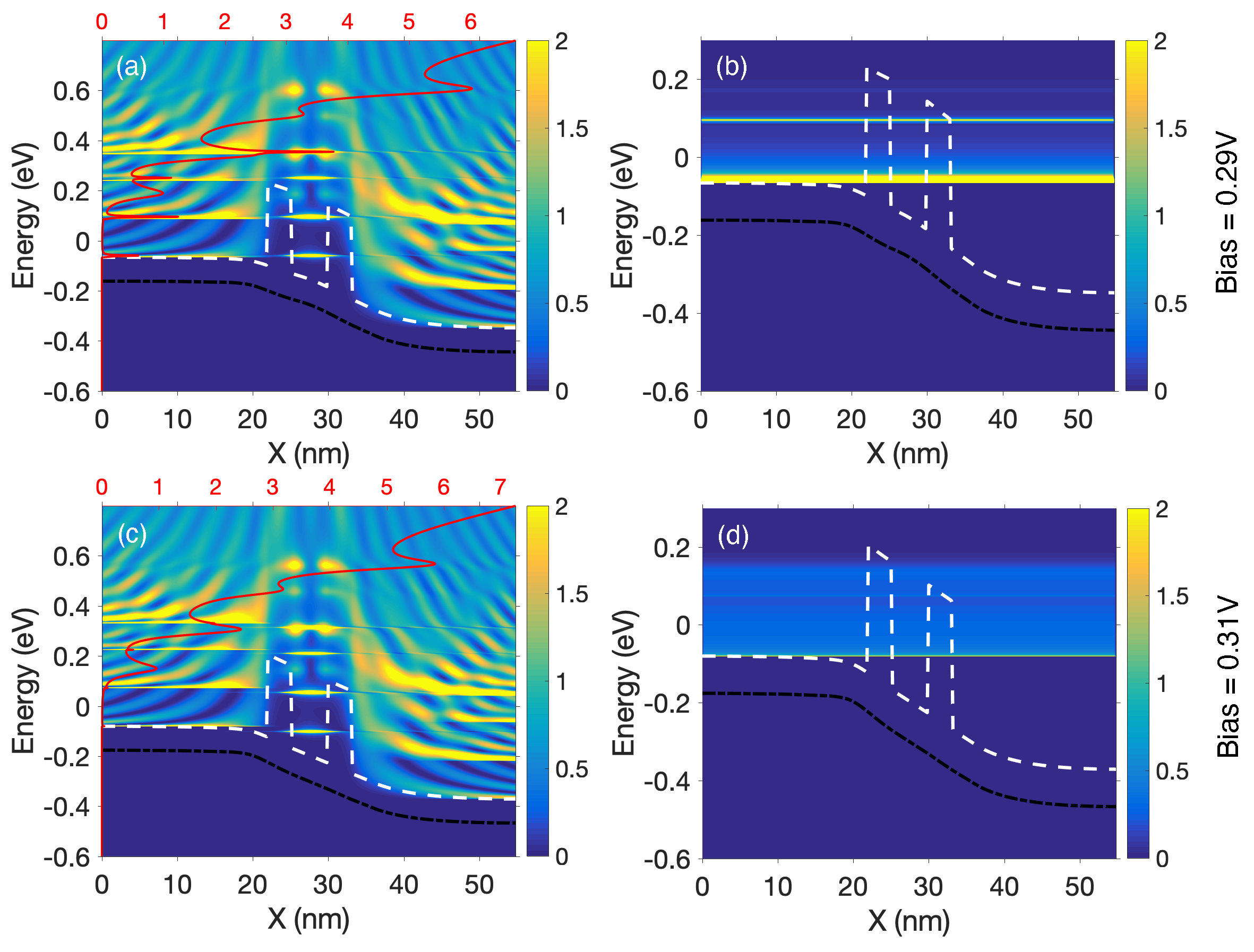
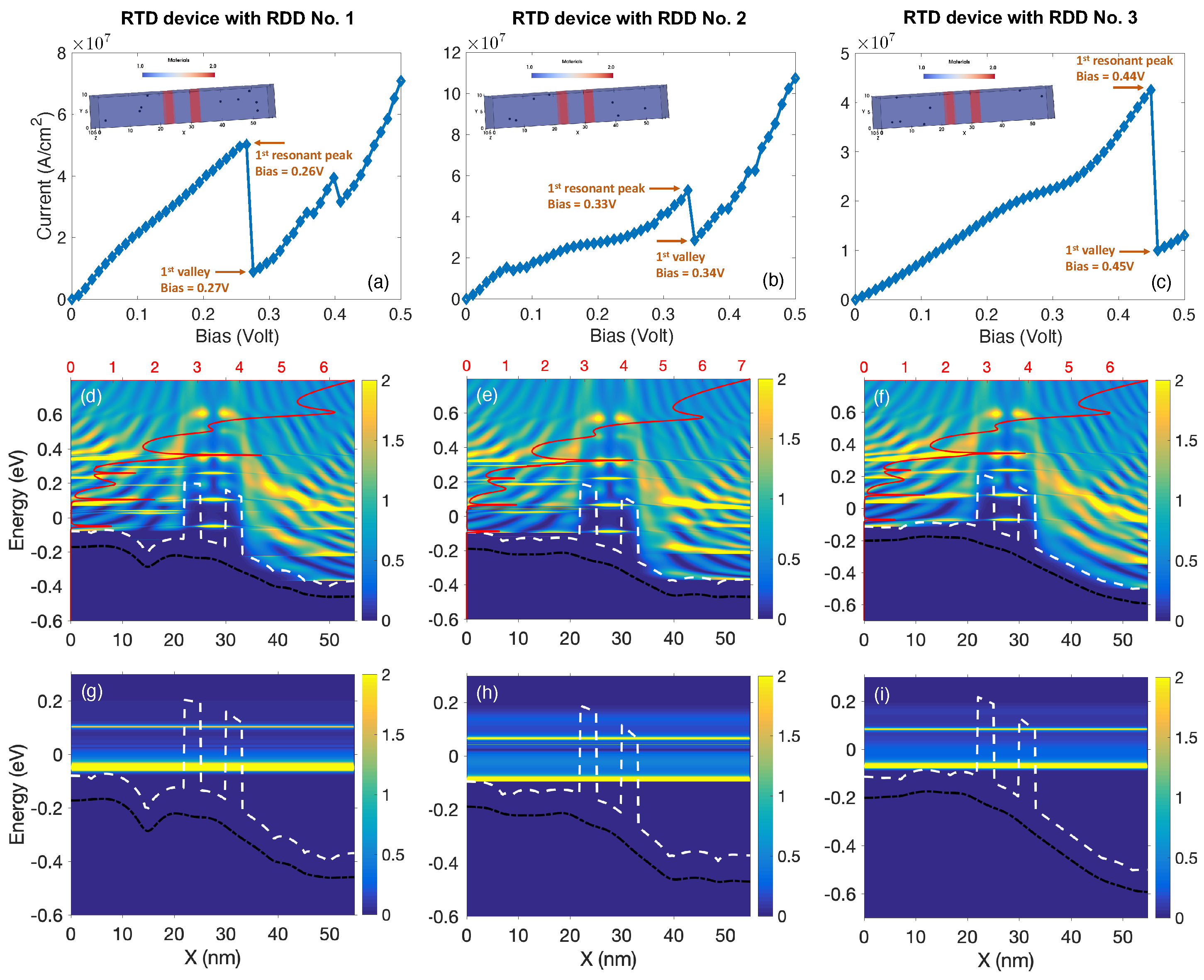
3.4. Resonant Tunneling Diodes (RTD)
4. Conclusions
Author Contributions
Funding
Institutional Review Board Statement
Informed Consent Statement
Data Availability Statement
Acknowledgments
Conflicts of Interest
References
- Moore, G. Cramming more components onto integrated circuits. Electronics 1965, 38, 114–117. [Google Scholar] [CrossRef]
- Berrada, S.; Carrillo-Nunez, H.; Lee, J.; Medina-Bailon, C.; Dutta, T.; Badami, O.; Adamu-Lema, F.; Thirunavukkarasu, V.; Georgiev, V.; Asenov, A. Nano-electronic Simulation Software (NESS): A flexible nano-device simulation platform. J. Comput. Electron. 2020, 19, 1031–1046. [Google Scholar] [CrossRef]
- Medina-Bailon, C.; Dutta, T.; Adamu-Lema, F.; Rezaei, A.; Nagy, D.; Gergiev, V.P.; Asenov, A. Nano-Electronic Simulation Software (NESS): A Novel Open-Source TCAD Simulation Environment. J. Microelectron. Manuf. 2020, 3. [Google Scholar] [CrossRef]
- Schaller, R.R. Moore’s law: Past, present and future. IEEE Spectr. 1997, 34, 52–59. [Google Scholar] [CrossRef]
- Lee, J.H. Bulk FinFETs: Design at 14 nm Node and Key Characteristics. In Nano Devices and Circuit Techniques for Low-Energy Applications and Energy Harvesting; Springer: Dordrecht, The Netherlands, 2016; pp. 33–64. [Google Scholar] [CrossRef]
- Bufler, F.M.; Ritzenthaler, R.; Mertens, H.; Eneman, G.; Mocuta, A.; Horiguchi, N. Performance Comparison of n–Type Si Nanowires, Nanosheets, and FinFETs by MC Device Simulation. IEEE Electron Device Lett. 2018, 39, 1628–1631. [Google Scholar] [CrossRef]
- Nagy, D.; Espiñeira, G.; Indalecio, G.; García-Loureiro, A.J.; Kalna, K.; Seoane, N. Benchmarking of FinFET, Nanosheet, and Nanowire FET Architectures for Future Technology Nodes. IEEE Access 2020, 8, 53196–53202. [Google Scholar] [CrossRef]
- Bhuwalka, K.K.; Schulze, J.; Eisele, I. Performance Enhancement of Vertical Tunnel Field-Effect Transistor with SiGe in the δp+ Layer. Jpn. J. Appl. Phys. 2004, 43, 4073–4078. [Google Scholar] [CrossRef]
- Wang, L.; Yu, E.; Taur, Y.; Asbeck, P. Design of Tunneling Field-Effect Transistors Based on Staggered Heterojunctions for Ultralow-Power Applications. IEEE Electron Device Lett. 2010, 31, 431–433. [Google Scholar] [CrossRef]
- Convertino, C.; Zota, C.B.; Schmid, H.; Ionescu, A.M.; Moselund, K.E. III–V heterostructure tunnel field-effect transistor. J. Phys. Condens. Matter 2018, 30, 264005. [Google Scholar] [CrossRef]
- Convertino, C.; Zota, C.B.; Schmid, H.; Caimi, D.; Czornomaz, L.; Ionescu, A.M.; Moselund, K.E. A hybrid III–V tunnel FET and MOSFET technology platform integrated on silicon. Nat. Electron. 2021, 4, 162–170. [Google Scholar] [CrossRef]
- Choi, W.Y.; Park, B.; Lee, J.D.; Liu, T.K. Tunneling Field-Effect Transistors (TFETs) With Subthreshold Swing (SS) Less Than 60 mV/dec. IEEE Electron Device Lett. 2007, 28, 743–745. [Google Scholar] [CrossRef]
- Salahuddin, S.; Datta, S. Use of Negative Capacitance to Provide Voltage Amplification for Low Power Nanoscale Devices. Nano Lett. 2008, 8, 405–410. [Google Scholar] [CrossRef] [PubMed]
- Liang, Y.; Zhu, Z.; Li, X.; Gupta, S.K.; Datta, S.; Narayanan, V. Utilization of Negative-Capacitance FETs to Boost Analog Circuit Performances. IEEE Trans. Very Large Scale Integr. (VLSI) Syst. 2019, 27, 2855–2860. [Google Scholar] [CrossRef]
- Sakib, F.I.; Hasan, M.A.; Hossain, M. Exploration of Negative Capacitance in Gate-All-Around Si Nanosheet Transistors. IEEE Trans. Electron Devices 2020, 67, 5236–5242. [Google Scholar] [CrossRef]
- Asada, M.; Suzuki, S.; Kishimoto, N. Resonant Tunneling Diodes for Sub-Terahertz and Terahertz Oscillators. Jpn. J. Appl. Phys. 2008, 47, 4375–4384. [Google Scholar] [CrossRef]
- Sun, J.P.; Haddad, G.I.; Mazumder, P.; Schulman, J.N. Resonant tunneling diodes: Models and properties. Proc. IEEE 1998, 86, 641–660. [Google Scholar] [CrossRef] [Green Version]
- Roberts, J.; Bagci, I.E.; Zawawi, M.A.M.; Sexton, J.; Hlbert, N.; Noori, Y.J.; Young, M.P.; Woodhead, C.S.; Missous, M.; Migliorato, M.A.; et al. Using Quantum Confinement to Uniquely Identify Devices. Sci. Rep. 2015, 5, 16456. [Google Scholar] [CrossRef] [Green Version]
- Leem, J.; Kim, M.; Choi, S.; Kim, S.R.; Kim, S.W.; Song, Y.; Young, R.; Kim, Y. Edible unclonable functions. Nat. Commun. 2020, 11. [Google Scholar] [CrossRef] [Green Version]
- McGrath, T.; Bagci, I.; Wang, Z.; Roedig, U.; Young, R. A PUF Taxonomy. Appl. Phys. Rev. 2019, 6. [Google Scholar] [CrossRef] [Green Version]
- Berrada, S.; Dutta, T.; Carrillo-Nunez, H.; Duan, M.; Adamu-Lema, F.; Lee, J.; Georgiev, V.; Medina-Bailon, C.; Asenov, A. NESS: New flexible Nano-Electronic Simulation Software. In Proceedings of the 2018 International Conference on Simulation of Semiconductor Processes and Devices (SISPAD), Austin, TX, USA, 24–26 September 2018; pp. 22–25. [Google Scholar] [CrossRef] [Green Version]
- Medina-Bailon, C.; Badami, O.; Carrillo-Nunez, H.; Dutta, T.; Nagy, D.; Adamu-Lema, F.; Georgiev, V.P.; Asenov, A. Enhanced Capabilities of the Nano-Electronic Simulation Software (NESS). In Proceedings of the 2020 International Conference on Simulation of Semiconductor Processes and Devices (SISPAD), Kobe, Japan, 23 September–6 October 2020; pp. 293–296. [Google Scholar] [CrossRef]
- Lee, J.; Badami, O.; Carrillo-Nuñez, H.; Berrada, S.; Medina-Bailon, C.; Dutta, T.; Adamu-Lema, F.; Georgiev, V.P.; Asenov, A. Variability predictions for the next technology generations of n-type SixGe1-x nanowire MOSFETs. Micromachines 2018, 9, 643. [Google Scholar] [CrossRef] [Green Version]
- Lee, J.; Berrada, S.; Carrillo-Nunez, H.; Medina-Bailon, C.; Adamu-Lema, F.; Georgiev, V.P.; Asenov, A. The impact of dopant diffusion on random dopant fluctuation in Si nanowire FETs: A quantum transport study. In Proceedings of the 2018 International Conference on Simulation of Semiconductor Processes and Devices (SISPAD), Austin, TX, USA, 24–26 September 2018; pp. 280–283. [Google Scholar] [CrossRef]
- Badami, O.; Medina-Bailon, C.; Berrada, S.; Carrillo-Nunez, H.; Lee, J.; Georgiev, V.; Asenov, A. Comprehensive Study of Cross-Section Dependent Effective Masses for Silicon Based Gate-All-Around Transistors. Appl. Sci. 2019, 9, 1895. [Google Scholar] [CrossRef] [Green Version]
- Scharfetter, D.L.; Gummel, H.K. Large-signal analysis of a silicon read diode oscillator. IEEE Trans. Electron Devices 1969, 16, 64–77. [Google Scholar] [CrossRef]
- Masetti, G.; Severi, M.; Solmi, S. Modeling of carrier mobility against carrier concentration in arsenic-, phosphorus-, and boron-doped silicon. IEEE Trans. Electron Devices 1983, 30, 764–769. [Google Scholar] [CrossRef]
- Yamaguchi, K. Field-dependent mobility model for two-dimensional numerical analysis of MOSFET’s. IEEE Trans. Electron Devices 1979, 26, 1068–1074. [Google Scholar] [CrossRef]
- Caughey, D.M.; Thomas, R. Carrier mobilities in silicon empirically related to doping and field. Proc. IEEE 1967, 55, 2192–2193. [Google Scholar] [CrossRef]
- Dutta, T.; Medina-Bailon, C.; Carrillo-Nuñez, H.; Badami, O.; Georgiev, V.; Asenov, A. Schrödinger Equation Based Quantum Corrections in Drift-Diffusion: A Multiscale Approach. In Proceedings of the 2019 IEEE 14th Nanotechnology Materials and Devices Conference (NMDC), Stockholm, Sweden, 27–30 October 2019; pp. 1–4. [Google Scholar] [CrossRef]
- Medina-Bailon, C.; Sadi, T.; Nedjalkov, M.; Lee, J.; Berrada, S.; Carrillo-Nuñez, H.; Georgiev, V.; Selberherr, S.; Asenov, A. Study of the 1D Scattering Mechanisms’ Impact on the Mobility in Si Nanowire Transistors. In Proceedings of the 2018 Joint International EUROSOI Workshop and International Conference on Ultimate Integration on Silicon (EUROSOI-ULIS), Granada, Spain, 19–21 March 2018; pp. 1–4. [Google Scholar] [CrossRef]
- Medina-Bailon, C.; Sadi, T.; Nedjalkov, M.; Lee, J.; Berrada, S.; Carrillo-Nuñez, H.; Georgiev, V.; Selberherr, S.; Asenov, A. Impact of the Effective Mass on the Mobility in Si Nanowire Transistors. In Proceedings of the 2018 International Conference on Simulation of Semiconductor Processes and Devices (SISPAD), Austin, TX, USA, 24–26 September 2018; pp. 297–300. [Google Scholar] [CrossRef] [Green Version]
- Medina-Bailon, C.; Sadi, T.; Nedjalkov, M.; Carrillo-Nunez, H.; Lee, J.; Badami, O.; Georgiev, V.; Selberherr, S.; Asenov, A. Mobility of Circular and Elliptical Si Nanowire Transistors Using a Multi-Subband 1D Formalism. IEEE Electron Device Lett. 2019, 40, 1571–1574. [Google Scholar] [CrossRef] [Green Version]
- Sadi, T.; Medina-Bailon, C.; Nedjalkov, M.; Lee, J.; Badami, O.; Berrada, S.; Carrillo-Nuñez, H.; Georgiev, V.; Selberherr, S.; Asenov, A. Simulation of the Impact of Ionized Impurity Scattering on the Total Mobility in Si Nanowire Transistors. Materials 2019, 12, 124. [Google Scholar] [CrossRef] [Green Version]
- Jin, S.; Tang, T.W.; Fischetti, M.V. Simulation of silicon nanowire transistors using Boltzmann transport equation under relaxation time approximation. IEEE Trans. Electron Devices 2008, 55, 727–736. [Google Scholar] [CrossRef]
- Sancho, M.; Sancho, J.; Sancho, J.; Rubio, J. Highly convergent schemes for the calculation of bulk and surface Green functions. J. Phys. F Met. Phys. 1985, 15, 851–858. [Google Scholar] [CrossRef]
- Luisier, M.; Schenk, A.; Fichtner, W. Quantum transport in two- and three-dimensional nanoscale transistors: Coupled mode effects in the nonequilibrium Greens function formalism. J. Appl. Phys. 2006, 100, 043713. [Google Scholar] [CrossRef] [Green Version]
- Svizhenko, A.; Anantram, M.P. Role of scattering in nanotransistors. IEEE Trans. Electron Devices 2003, 50, 1459–1466. [Google Scholar] [CrossRef]
- Medina-Bailon, C.; Carrillo-Nunez, H.; Lee, J.; Sampedro, C.; Padilla, J.L.; Donetti, L.; Georgiev, V.; Gamiz, F.; Asenov, A. Quantum Enhancement of a S/D Tunneling Model in a 2D MS-EMC Nanodevice Simulator: NEGF Comparison and Impact of Effective Mass Variation. Micromachines 2020, 11, 204. [Google Scholar] [CrossRef] [PubMed] [Green Version]
- Carrillo-Nuñez, H.; Lee, J.; Berrada, S.; Medina-Bailón, C.; Adamu-Lema, F.; Luisier, M.; Asenov, A.; Georgiev, V.P. Random dopant-induced variability in Si-InAs nanowire tunnel FETs: A quantum transport simulation study. IEEE Electron Device Lett. 2018, 39, 1473–1476. [Google Scholar] [CrossRef] [Green Version]
- Carrillo-Nuñez, H.; Medina-Bailón, C.; Georgiev, V.P.; Asenov, A. Full-band quantum transport simulation in the presence of hole-phonon interactions using a mode-space k· p approach. Nanotechnology 2020, 32, 020001. [Google Scholar] [CrossRef]
- Badami, O.; Berrada, S.; Carrillo-Nunez, H.; Medina-Bailon, C.; Georgiev, V.; Asenov, A. Surface Roughness Scattering in NEGF using self-energy formulation. In Proceedings of the 2019 International Conference on Simulation of Semiconductor Processes and Devices (SISPAD), Udine, Italy, 4–6 September 2019; pp. 1–4. [Google Scholar] [CrossRef]
- Badami, O.; Sadi, T.; Adamu-Lema, F.; Lapham, P.; Mu, D.; Georgiev, V.; Ding, J.; Asenov, A. A Kinetic Monte Carlo study of retention time in a POM molecule-based flash memory. IEEE Trans. Nanotechnol. 2020, 19, 704–710. [Google Scholar] [CrossRef]
- Lapham, P.; Badami, O.; Medina-Bailon, C.; Adamu-Lema, F.; Dutta, T.; Nagy, D.; Georgiev, V.; Asenov, A. A Combined First Principles and Kinetic Monte Carlo study of Polyoxometalate based Molecular Memory Devices. In Proceedings of the 2020 International Conference on Simulation of Semiconductor Processes and Devices (SISPAD), Kobe, Japan, 23 September–6 October 2020; pp. 273–276. [Google Scholar] [CrossRef]
- Cristoloveanu, S. How many gates do we need in a transistor? In Proceedings of the 2007 International Semiconductor Conference, Sinaia, Romania, 15–17 October 2007; pp. 3–10. [Google Scholar] [CrossRef]
- Yu, B.; Wang, H.; Yang, C.; Asbeck, P.; Taur, Y. Scaling of nanowire transistors. IEEE Trans. Electron Devices 2008, 55, 2846–2858. [Google Scholar] [CrossRef]
- Ferry, D.K.; Gilbert, M.J.; Akis, R. Some considerations on nanowires in nanoelectronics. IEEE Trans. Electron Devices 2008, 55, 2820–2826. [Google Scholar] [CrossRef] [Green Version]
- Appenzeller, J.; Knoch, J.; Bjork, M.T.; Riel, H.; Schmid, H.; Riess, W. Toward nanowire electronics. IEEE Trans. Electron Devices 2008, 55, 2827–2845. [Google Scholar] [CrossRef] [Green Version]
- Lu, W.; Xie, P.; Lieber, C.M. Nanowire transistor performance limits and applications. IEEE Trans. Electron Devices 2008, 55, 2859–2876. [Google Scholar] [CrossRef]
- Al-Ameri, T.; Georgiev, V.P.; Adamu-Lema, F.; Asenov, A. Simulation study of vertically stacked lateral Si nanowires transistors for 5-nm CMOS applications. IEEE J. Electron Devices Soc. 2017, 5, 466–472. [Google Scholar] [CrossRef]
- Selvakumar, C.; Hecht, B. SiGe-channel n-MOSFET by germanium implantation. IEEE Electron Device Lett. 1991, 12, 444–446. [Google Scholar] [CrossRef]
- Lee, J.; Shin, M. Performance assessment of III–V channel ultra-thin-body Schottky-barrier MOSFETs. IEEE Electron Device Lett. 2014, 35, 726–728. [Google Scholar] [CrossRef]
- Vasen, T.; Ramvall, P.; Afzalian, A.; Thelander, C.; Dick, K.; Holland, M.; Doornbos, G.; Wang, S.; Oxland, R.; Vellianitis, G.; et al. InAs nanowire GAA n-MOSFETs with 12–15 nm diameter. In Proceedings of the 2016 IEEE Symposium on VLSI Technology, Honolulu, HI, USA, 14–16 June 2016; pp. 1–2. [Google Scholar] [CrossRef]
- Grillet, C.; Logoteta, D.; Cresti, A.; Pala, M.G. Assessment of the Electrical Performance of Short Channel InAs and Strained Si Nanowire FETs. IEEE Trans. Electron Devices 2017, 64, 2425–2431. [Google Scholar] [CrossRef]
- Marquez, C.; Salazar, N.; Gity, F.; Navarro, C.; Mirabelli, G.; Galdon, J.C.; Duffy, R.; Navarro, S.; Hurley, P.K.; Gamiz, F. Investigating the transient response of Schottky barrier back-gated MoS2 transistors. 2D Mater. 2020, 7, 025040. [Google Scholar] [CrossRef]
- Knobloch, T.; Illarionov, Y.Y.; Ducry, F.; Schleich, C.; Wachter, S.; Watanabe, K.; Taniguchi, T.; Mueller, T.; Waltl, M.; Lanza, M.; et al. The performance limits of hexagonal boron nitride as an insulator for scaled CMOS devices based on two-dimensional materials. Nat. Electron. 2021, 4, 98–108. [Google Scholar] [CrossRef]
- Alher, M.A.; Mosleh, A.; Cousar, L.; Dou, W.; Grant, P.; Ghetmiri, S.A.; Al-Kabi, S.; Du, W.; Benamara, M.; Li, B.; et al. CMOS compatible growth of high quality Ge, SiGe and SiGeSn for photonic device applications. ECS Trans. 2015, 69, 269. [Google Scholar] [CrossRef]
- IEEE International Roadmap for Devices and Systems (IRDS). 2016. Available online: https://irds.ieee.org/reports (accessed on 25 September 2018).
- Al-Ameri, T.; Georgiev, V.P.; Sadi, T.; Wang, Y.; Adamu-Lema, F.; Wang, X.; Amoroso, S.M.; Towie, E.; Brown, A.; Asenov, A. Impact of quantum confinement on transport and the electrostatic driven performance of silicon nanowire transistors at the scaling limit. Solid State Electron. 2017, 129, 73–80. [Google Scholar] [CrossRef] [Green Version]
- Chindalore, G.; Hareland, S.A.; Jallepalli, S.A.; Tasch, A.F.; Maziar, C.M.; Chia, V.K.F.; Smith, S. Experimental determination of threshold voltage shifts due to quantum mechanical effects in MOS electron and hole inversion layers. IEEE Electron Device Lett. 2007, 18, 206–208. [Google Scholar] [CrossRef]
- Takeda, H.; Mori, N. Three-dimensional quantum transport simulation of ultra-small FinFETs. J. Comput. Electron. 2005, 4, 31–34. [Google Scholar] [CrossRef]
- Wang, Y.; Al-Ameri, T.; Wang, X.; Georgiev, V.P.; Towie, E.; Amoroso, S.M.; Brown, A.R.; Cheng, B.; Reid, D.; Riddet, C.; et al. Simulation study of the impact of quantum confinement on the electrostatically driven performance of n-type nanowire transistors. IEEE Trans. Electron Devices 2015, 62, 3229–3236. [Google Scholar] [CrossRef]
- Wong, H.S. Beyond the conventional transistor. IBM J. Res. Dev. 2002, 46, 133–168. [Google Scholar] [CrossRef]
- Lee, C.; Nazarov, A.; Ferain, I.; Akhavan, N.D.; Yan, R.; Razavi, P.; Yu, R.; Doria, R.; Colinge, J. Low subthreshold slope in junctionless multigate transistors. J. Appl. Phys. 2010, 96, 102106. [Google Scholar] [CrossRef]
- Ionescu, A.; Riel, H. Tunnel field-effect transistors as energy-efficient electronic switches. Nature 2011, 479, 329–337. [Google Scholar] [CrossRef] [PubMed]
- Carrillo-Nunez, H.; Luisier, M.; Schenk, A. Analysis of InAs-Si heterojunction nanowire tunnel FETs: Extreme confinement vs. bulk. Solid State Electron. 2015, 113, 61–63. [Google Scholar] [CrossRef] [Green Version]
- Medina-Bailon, C.; Padilla, J.; Sampedro, C.; Alper, C.; Gámiz, F.; Ionescu, A. Implementation of Band–to–Band Tunneling Phenomena in a Multi–Subband Ensemble Monte Carlo Simulator: Application to Silicon TFETs. IEEE Trans. Electron Devices 2017, 64, 3084–3091. [Google Scholar] [CrossRef]
- Sentaurus Process Version O-2018.06. [Synopsys, Inc., 2018]. 2018. Available online: https://www.synopsys.com/silicon/tcad/process-simulation/sentaurus-process.html (accessed on 25 September 2018).
- Björk, M.; Schmid, H.; Bessire, C.; Moselund, K.; Ghoneim, H.; Karg, S.; Lörtscher, E.; Riel, H. Si–InAs heterojunction Esaki tunnel diodes with high current densities. Appl. Phys. Lett. 2010, 97, 163501. [Google Scholar] [CrossRef]
- Riel, H.; Moselund, K.; Bessire, C.; Björk, M.; Schenk, A.; Ghoneim, H.; Schmid, H. InAs-Si heterojunction nanowire tunnel diodes and tunnel FETs. In Proceedings of the 2012 International Electron Devices Meeting (IEDM), San Francisco, CA, USA, 10–13 December 2012; pp. 16.6.1–16.6.4. [Google Scholar] [CrossRef]
- Carrillo-Nunez, H.; Rhyner, R.; Luisier, M.; Schenk, A. Effect of surface roughness and phonon scattering on extremely narrow InAs-Si Nanowire TFETs. In Proceedings of the 2016 46th European Solid-State Device Research Conference (ESSDERC), Lausanne, Switzerland, 12–15 September 2016; pp. 188–191. [Google Scholar] [CrossRef]
- Pahwa, G.; Dutta, T.; Agarwal, A.; Khandelwal, S.; Salahuddin, S.; Hu, C.; Chauhan, Y.S. Analysis and Compact Modeling of Negative Capacitance Transistor with High ON-Current and Negative Output Differential Resistance–Part I: Model Description. IEEE Trans. Electron Devices 2016, 63, 4981–4985. [Google Scholar] [CrossRef]
- Krivokapic, Z.; Rana, U.; Galatage, R.; Razavieh, A.; Aziz, A.; Liu, J.; Shi, J.; Kim, H.; Sporer, R.; Serrao, C.; et al. 14nm Ferroelectric FinFET Technology with Steep Subthreshold Slope for Ultra Low Power Applications. In Proceedings of the IEEE International Electron Devices Meeting (IEDM), San Francisco, CA, USA, 2–6 December 2017. [Google Scholar]
- Xu, Q.; Liu, X.; Wan, B.; Yang, Z.; Li, F.; Lu, J.; Hu, G.; Pan, C.; Wang, Z.L. In2O3 nanowire field-effect transistors with Sub-60 mV/dec subthreshold swing stemming from negative capacitance and their logic applications. ACS Nano 2018, 12, 9608–9616. [Google Scholar] [CrossRef]
- Pahwa, G.; Dutta, T.; Agarwal, A.; Chauhan, Y.S. Designing Energy Efficient and Hysteresis Free Negative Capacitance FinFET with Negative DIBL and 3.5X ION using Compact Modeling Approach. In Proceedings of the IEEE European Solid-State Device Research Conference (ESSDERC), Lausanne, Switzerland, 12–15 September 2016; pp. 41–46. [Google Scholar]
- Dutta, T.; Pahwa, G.; Agarwal, A.; Chauhan, Y.S. Impact of Process Variations on Negative Capacitance FinFET Devices and Circuits. IEEE Electron Device Lett. 2018, 39, 147–150. [Google Scholar] [CrossRef]
- Dutta, T.; Georgiev, V.P.; Asenov, A. Random Discrete Dopant Induced Variability in Negative Capacitance Transistors. In Proceedings of the Joint International EUROSOI Workshop and International Conference on Ultimate Integration on Silicon (EUROSOI-ULIS), Granada, Spain, 19–21 March 2018. [Google Scholar]
- Lee, H.P.; Su, P. Suppressed Fin-LER Induced Variability in Negative Capacitance FinFETs. IEEE Electron Device Lett. 2017, 38, 1492–1495. [Google Scholar] [CrossRef]
- Dutta, T.; Georgiev, V.P.; Asenov, A. Interplay of RDF and Gate LER Induced Statistical Variability in Negative Capacitance FETs. In Proceedings of the International Conference on Simulation of Semiconductor Processes and Devices (SISPAD), Austin, TX, USA, 24–26 September 2018; pp. 262–265. [Google Scholar]
- Dutta, T.; Pahwa, G.; Trivedi, A.R.; Sinha, S.; Agarwal, A.; Chauhan, Y.S. Performance Evaluation of 7-nm Node Negative Capacitance FinFET-Based SRAM. IEEE Electron Device Lett. 2017, 38, 1161–1164. [Google Scholar] [CrossRef]
- Dutta, T.; Georgiev, V.P.; Asenov, A. Vmin Prediction for Negative Capacitance MOSFET based SRAM. In Proceedings of the Joint International EUROSOI Workshop and International Conference on Ultimate Integration on Silicon (EUROSOI-ULIS), Caen, France, 1–30 September 2020. [Google Scholar]
- Alam, M.A.; Si, M.; Ye, P.D. A critical review of recent progress on negative capacitance field-effect transistors. Appl. Phys. Lett. 2019, 114, 090401. [Google Scholar] [CrossRef] [Green Version]
- Devonshire; Frederick, A. XCVI. Theory of barium titanate: Part I. Lond. Edinb. Dublin Philos. Mag. J. Sci. 1949, 40, 1040–1063. [Google Scholar] [CrossRef]
- Landau, L.D.; Khalatnikov, I.M. On the anomalous absorption ofsound near a second order phase transition point. Dok. Akad. Nauk SSSR 1954, 96, 469–472. [Google Scholar]
- Hoffmann, M.; Max, B.; Mittmann, T.; Schroeder, U.; Slesazeck, S.; Mikolajick, T. Demonstration of high-speed hysteresis-free negative capacitance in ferroelectric Hf0.5 Zr0.5 O2. In Proceedings of the 2018 IEEE International Electron Devices Meeting (IEDM), San Francisco, CA, USA, 1–5 December 2018; pp. 31–36. [Google Scholar]
- Yadav, A.K.; Nguyen, K.X.; Hong, Z.; García-Fernández, P.; Aguado-Puente, P.; Nelson, C.T.; Das, S.; Prasad, B.; Kwon, D.; Cheema, S.; et al. Spatially resolved steady-state negative capacitance. Nature 2019, 565, 468–471. [Google Scholar] [CrossRef] [PubMed] [Green Version]
- Pahwa, G.; Dutta, T.; Agarwal, A.; Chauhan, Y.S. Physical Insights on Negative Capacitance Transistors in Non-hysteresis and Hysteresis Regimes: MFMIS Versus MFIS Structures. IEEE Trans. Electron Devices 2018, 65, 867–873. [Google Scholar] [CrossRef]
- Khan, A.I.; Radhakrishna, U.; Chatterjee, K.; Salahuddin, S.; Antoniadis, D.A. Negative capacitance behavior in a leaky ferroelectric. IEEE Trans. Electron Devices 2016, 63, 4416–4422. [Google Scholar] [CrossRef]
- Lee, M.; Fan, S.T.; Tang, C.H.; Chen, P.G.; Chou, Y.C.; Chen, H.H.; Kuo, J.Y.; Xie, M.J.; Liu, S.N.; Liao, M.H.; et al. Physical thickness 1.x nm ferroelectric HfZrOx negative capacitance FETs. In Proceedings of the 2016 IEEE International Electron Devices Meeting (IEDM), San Francisco, CA, USA, 3–7 December 2016; pp. 12.1.1–12.1.4. [Google Scholar]
- Kwon, D.; Liao, Y.H.; Lin, Y.K.; Duarte, J.P.; Chatterjee, K.; Tan, A.J.; Yadav, A.K.; Hu, C.; Krivokapic, Z.; Salahuddin, S. Response speed of negative capacitance FinFETs. In Proceedings of the 2018 IEEE Symposium on VLSI Technology, Honolulu, HI, USA, 18–22 June 2018; pp. 49–50. [Google Scholar]
- Seo, J.; Lee, J.; Shin, M. Analysis of drain-induced barrier rising in short-channel negative-capacitance FETs and its applications. IEEE Trans. Electron Devices 2017, 64, 1793–1798. [Google Scholar] [CrossRef]
- Zhou, H.; Kwon, D.; Sachid, A.B.; Liao, Y.; Chatterjee, K.; Tan, A.J.; Yadav, A.K.; Hu, C.; Salahuddin, S. Negative capacitance, n-channel, Si FinFETs: Bi-directional sub-60 mV/dec, negative DIBL, negative differential resistance and improved short channel effect. In Proceedings of the 2018 IEEE Symposium on VLSI Technology, Honolulu, HI, USA, 18–22 June 2018; pp. 53–54. [Google Scholar]
- Lee, S.Y.; Chen, H.W.; Shen, C.H.; Kuo, P.Y.; Chung, C.C.; Huang, Y.E.; Chen, H.Y.; Chao, T.S. Effect of seed layer on gate-all-around poly-Si nanowire negative-capacitance FETs with MFMIS and MFIS structures: Planar capacitors to 3-D FETs. IEEE Trans. Electron Devices 2020, 67, 711–716. [Google Scholar] [CrossRef]
- Lee, M.; Chen, P.G.; Fan, S.T.; Chou, Y.C.; Kuo, C.Y.; Tang, C.H.; Chen, H.H.; Gu, S.S.; Hong, R.C.; Wang, Z.Y.; et al. Ferroelectric Al: HfO2 negative capacitance FETs. In Proceedings of the IEEE International Electron Devices Meeting (IEDM), San Francisco, CA, USA, 2–6 December 2017. [Google Scholar]
- Chang, L.L.; Esaki, L.; Tsu, R. Resonant tunneling in semiconductor double barriers. Appl. Phys. Lett. 1974, 24, 593–595. [Google Scholar] [CrossRef]
- Teran, F.J.; Martín, M.D.; Calleja, J.M.; Viña, L.; Eaves, L.; Henini, M. Carrier injection effects on exciton dynamics in GaAs/AlAs resonant-tunneling diodes. EPL (Europhys. Lett.) 2009, 85, 67010. [Google Scholar] [CrossRef]
- Tsu, R.; Esaki, L. Tunneling in a finite superlattice. Appl. Phys. Lett. 1973, 22, 562–564. [Google Scholar] [CrossRef]
- Hänggi, M.; Chua, L.O. Cellular neural networks based on resonant tunnelling diodes. Int. J. Circuit Theory Appl. 2001, 29, 487–504. [Google Scholar] [CrossRef]
- Feiginov, M.; Sydlo, C.; Cojocari, O.; Meissner, P. Resonant-tunnelling-diode oscillators operating at frequencies above 1.1 THz. Appl. Phys. Lett. 2011, 99, 233506. [Google Scholar] [CrossRef]
- Ishigaki, K.; Shiraishi, M.; Suzuki, S.; Asada, M.; Nishiyama, N.; Arai, S. Direct intensity modulation and wireless data transmission characteristics of terahertz-oscillating resonant tunnelling diodes. Electron. Lett. 2012, 48, 582–583. [Google Scholar] [CrossRef]
- Maekawa, T.; Kanaya, H.; Suzuki, S.; Asada, M. Frequency increase in terahertz oscillation of resonant tunnelling diode up to 1.55 THz by reduced slot-antenna length. Electron. Lett. 2014, 50, 1214–1216. [Google Scholar] [CrossRef]
- Diebold, S.; Nishio, K.; Nishida, Y.; Kim, J.Y.; Tsuruda, K.; Mukai, T.; Fujita, M.; Nagatsuma, T. High-speed error-free wireless data transmission using a terahertz resonant tunnelling diode transmitter and receiver. Electron. Lett. 2016, 52, 1999–2001. [Google Scholar] [CrossRef]
- Oshima, N.; Hashimoto, K.; Suzuki, S.; Asada, M. Wireless data transmission of 34 Gbit/s at a 500-GHz range using resonant-tunnelling-diode terahertz oscillator. Electron. Lett. 2016, 52, 1897–1898. [Google Scholar] [CrossRef]
- Oshima, N.; Hashimoto, K.; Suzuki, S.; Asada, M. Terahertz Wireless Data Transmission With Frequency and Polarization Division Multiplexing Using Resonant-Tunneling-Diode Oscillators. IEEE Trans. Terahertz Sci. Technol. 2017, 7, 593–598. [Google Scholar] [CrossRef]
- Park, J.; Lee, J.; Yang, K. A 24-GHz Low-Power RTD-Based ON–OFF Keying Oscillator With an RTD Pair Configuration. IEEE Microw. Wirel. Compon. Lett. 2018, 28, 521–523. [Google Scholar] [CrossRef]
- Kasagi, K.; Suzuki, S.; Asada, M. Large-scale array of resonant-tunneling-diode terahertz oscillators for high output power at 1 THz. J. Appl. Phys. 2019, 125, 151601. [Google Scholar] [CrossRef]
- Feiginov, M. Frequency Limitations of Resonant-Tunnelling Diodes in Sub-THz and THz Oscillators and Detectors. J. Infrared Millim. Terahertz Waves 2019, 40, 365–394. [Google Scholar] [CrossRef] [Green Version]
- Bernardo-Gavito, R.; Bagci, I.E.; Roberts, J.; Sexton, J.; Astbury, B.; Shokeir, H.; McGrath, T.; Noori, Y.J.; Woodhead, C.S.; Missous, M.; et al. Extracting random numbers from quantum tunnelling through a single diode. Sci. Rep. 2017, 7, 17879. [Google Scholar] [CrossRef] [PubMed] [Green Version]
- Bagci, I.E.; McGrath, T.; Barthelmes, C.; Dean, S.; Bernardo Gavito, R.; Young, R.J.; Roedig, U. Resonant-Tunnelling Diodes as PUF Building Blocks. IEEE Trans. Emerg. Top. Comput. 2019. [Google Scholar] [CrossRef] [Green Version]
- Svizhenko, A.; Anantram, M.; Govindan, T.; Biegel, B.; Venugopal, R. Two-dimensional quantum mechanical modeling of nanotransistors. J. Appl. Phys. 2002, 91, 2343–2354. [Google Scholar] [CrossRef] [Green Version]
- Anantram, M.P.; Lundstrom, M.S.; Nikonov, D.E. Modeling of Nanoscale Devices. Proc. IEEE 2008, 96, 1511–1550. [Google Scholar] [CrossRef] [Green Version]


Publisher’s Note: MDPI stays neutral with regard to jurisdictional claims in published maps and institutional affiliations. |
© 2021 by the authors. Licensee MDPI, Basel, Switzerland. This article is an open access article distributed under the terms and conditions of the Creative Commons Attribution (CC BY) license (https://creativecommons.org/licenses/by/4.0/).
Share and Cite
Medina-Bailon, C.; Dutta, T.; Rezaei, A.; Nagy, D.; Adamu-Lema, F.; Georgiev, V.P.; Asenov, A. Simulation and Modeling of Novel Electronic Device Architectures with NESS (Nano-Electronic Simulation Software): A Modular Nano TCAD Simulation Framework. Micromachines 2021, 12, 680. https://doi.org/10.3390/mi12060680
Medina-Bailon C, Dutta T, Rezaei A, Nagy D, Adamu-Lema F, Georgiev VP, Asenov A. Simulation and Modeling of Novel Electronic Device Architectures with NESS (Nano-Electronic Simulation Software): A Modular Nano TCAD Simulation Framework. Micromachines. 2021; 12(6):680. https://doi.org/10.3390/mi12060680
Chicago/Turabian StyleMedina-Bailon, Cristina, Tapas Dutta, Ali Rezaei, Daniel Nagy, Fikru Adamu-Lema, Vihar P. Georgiev, and Asen Asenov. 2021. "Simulation and Modeling of Novel Electronic Device Architectures with NESS (Nano-Electronic Simulation Software): A Modular Nano TCAD Simulation Framework" Micromachines 12, no. 6: 680. https://doi.org/10.3390/mi12060680