Formation of Periodic Nanoridge Patterns by Ultrashort Single Pulse UV Laser Irradiation of Gold

 , , and
Abstract
:
1. Introduction
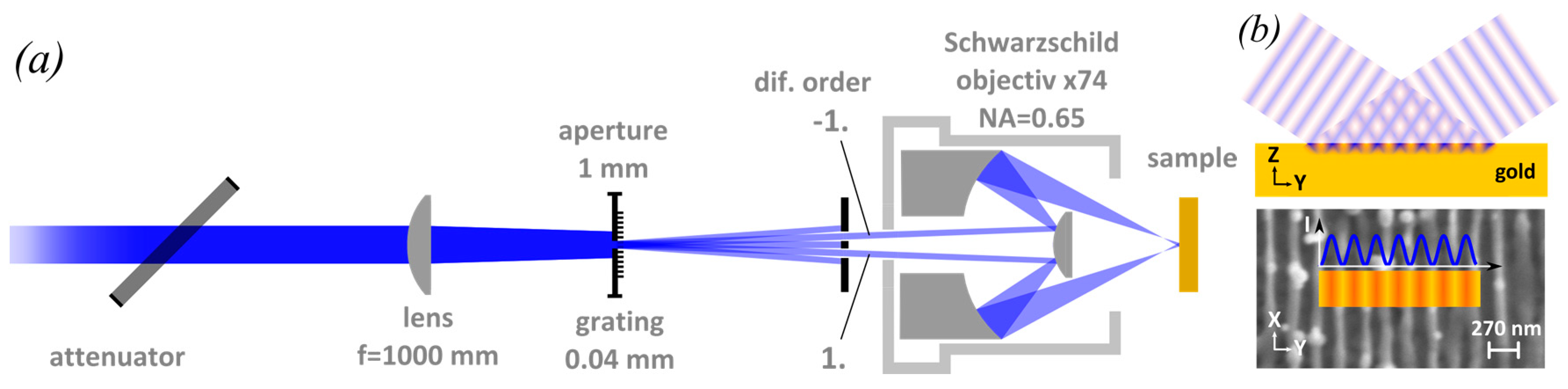
2. Experiment
3. Theory
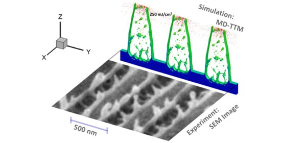
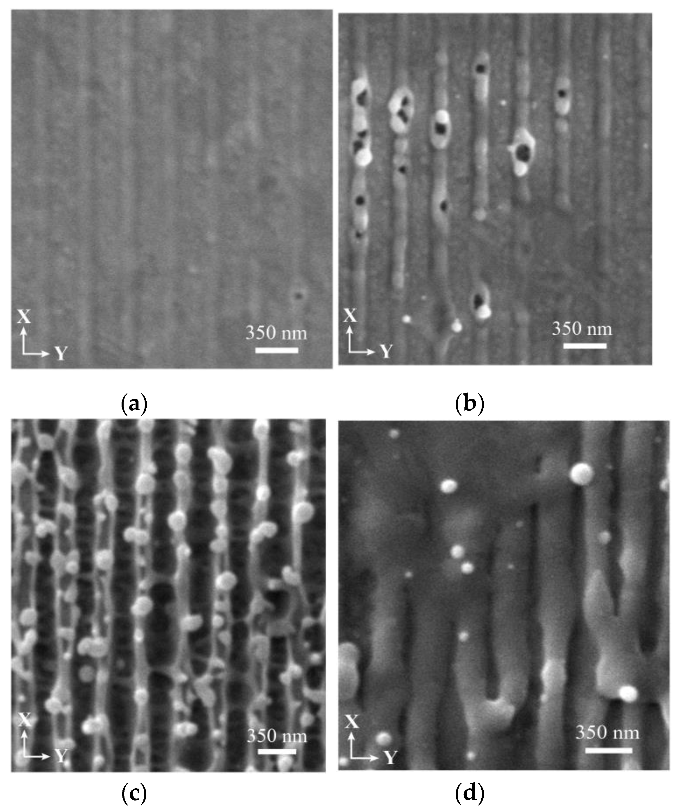
4. Results and Discussions
5. Conclusions
Author Contributions
Funding
Acknowledgments
Conflicts of Interest
References
- Bonse, J.; Höhm, S.; Kirner, S.V.; Rosenfeld, A.; Krüger, J. Laser-Induced Periodic Surface Structures—A Scientific Evergreen. IEEE J. Selec. Top. Quantum Electron. 2017, 23, 9000615. [Google Scholar] [CrossRef]
- Reif, J.; Varlamova, O.; Varlamov, S.; Bestehorn, M. The role of asymmetric excitation in self-organized nanostructure formation upon femtosecond laser ablation. Appl. Phys. A 2011, 104, 969–973. [Google Scholar] [CrossRef]
- Drogowska-Horna, K.A.; Mirza, I.; Rodriguez, A.; Kovaříček, P.; Sládek, J.; Derrien, T.J.Y.; Gedvilas, M.; Račiukaitis, G.; Frank, O.; Bulgakova, N.M. Periodic surface functional group density on graphene via laser-induced substrate patterning at Si/SiO2 interface. Nano Res. 2020, 13, 2332–2339. [Google Scholar] [CrossRef]
- Miyaji, G.; Miyazaki, K. Fabrication of 50-nm period gratings on GaN in air through plasmonic near-field ablation induced by ultraviolet femtosecond laser pulses. Opt. Express 2016, 24, 4648–4653. [Google Scholar] [CrossRef]
- Murphy, R.D.; Torralva, B.; Adams, D.P.; Yalisove, S.M. Polarization dependent formation of femtosecond laser-induced periodic surface structures near stepped features. Appl. Phys. Lett. 2014, 104, 231117. [Google Scholar] [CrossRef]
- Terekhin, P.N.; Benhayoun, O.; Weber, S.T.; Ivanov, D.S.; Garcia, M.E.; Rethfeld, B. Influence of Surface Plasmon Polaritons on Laser Energy Absorption and Structuring of Surfaces. Appl. Surf. Sci. 2020, 512, 144420. [Google Scholar] [CrossRef] [Green Version]
- Ilcisin, K.J.; Fedosejevs, R. Direct production of gratings on plastic substrates using 248-nm KrF laser radiation. Appl. Opt. 1987, 26, 396. [Google Scholar] [CrossRef]
- Phillips, H.M.; Sauerbrey, R.A. Excimer-laser-produced nanostructures in polymers. Opt. Eng. 1993, 32, 2424. [Google Scholar] [CrossRef]
- Lasagni, A.F.; Acevedo, D.F.; Barbero, C.A.; Mücklich, F. One-Step Production of Organized Surface Architectures on Polymeric Materials by Direct Laser Interference Patterning. Adv. Eng. Mat. 2007, 9, 99. [Google Scholar] [CrossRef]
- Wang, D.; Wang, Z.; Zhang, Z.; Yue, Y.; Li, D.; Qiu, R.; Maple, C. Both antireflection and superhydrophobicity structures achieved by direct laser interference nanomanufacturing. J. Appl. Phys. 2014, 115, 233101. [Google Scholar] [CrossRef] [Green Version]
- Beckemper, S.; Huang, J.; Gillner, A.; Wang, K. Generation of periodic micro- and nano-structures by parameter-controlled three-beam laser interference technique. J. Laser Micro Nanoen. 2011, 6, 49. [Google Scholar] [CrossRef]
- Tsunetomo, K.; Koyama, T. Direct formation of a surface-relief grating on glass by ultraviolet–visible laser irradiation. Opt. Lett. 1997, 4, 411–413. [Google Scholar] [CrossRef] [PubMed]
- Simon, P.; Ihlemann, J. Machining of submicron structures on metals and semiconductors by ultrashort UV-laser pulses. Appl. Phys. A 1996, 63, 505–508. [Google Scholar] [CrossRef]
- Kaakkunen, J.J.J.; Paivasaari, K.; Vahimaa, P. Fabrication of large-area hole arrays using high-efficiency two-grating interference system and femtosecond laser ablation. Appl. Phys. A 2011, 103, 267–270. [Google Scholar] [CrossRef]
- Nakata, Y.; Momoo, K.; Miyanaga, N.; Hiromoto, T.; Tsuchida, K. Organized metamaterials comprised of gold nanoneedles in a lattice generated on silicon (100) wafer substrates by interfering femtosecond laser processing. Appl. Phys. A 2013, 112, 173–177. [Google Scholar] [CrossRef]
- Ivanov, D.S.; Lipp, V.P.; Veiko, V.P.; Jakovlev, E.; Rethfeld, B.; Garcia, M.E. Molecular Dynamics Study of the Short Laser Pulse Ablation: Quality and Efficiency in Production. Appl. Phys. A 2014, 117, 2133–2141. [Google Scholar] [CrossRef]
- Rethfeld, B.; Ivanov, D.S.; Garcia, M.E.; Anisimov, S.I. Modelling Ultrafast Laser Ablation. J. Phys. D 2017, 50, 193001. [Google Scholar] [CrossRef]
- Inogamov, N.A.; Zhakhovsky, V.V.; Khokhlov, V.A.; Petrov, Y.V.; Migdal, K.P. Solitary Nanostructures Produced by Ultrashort Laser Pulse. Nanoscale Res. Lett. 2016, 11, 177. [Google Scholar] [CrossRef] [Green Version]
- Apel, O.; Beinhorn, F.; Ihlemann, J.; Klein-Wiele, J.-H.; Marowsky, G.; Simon, P. Periodic nanostructures. Z. Phys. Chem. 2000, 214, 1233. [Google Scholar] [CrossRef]
- Molotokaitė, E.; Gedvilas, M.; Račiukaitis, G.; Girdauskas, V. Picosecond laser beam interference ablation of thin metal film on glass substrate. J. Laser Micro Nanoen. 2010, 5, 74–79. [Google Scholar] [CrossRef]
- Höche, T.; Böhme, R.; Gerlach, J.W.; Frost, F.; Zimmer, K.; Rauschenbach, B. Semiconductor Nanowires Prepared by Diffraction-Mask-Projection Excimer-Laser Patterning. Nano Lett. 2004, 4, 895–897. [Google Scholar] [CrossRef]
- Nakata, Y.; Matsuba, Y.; Miyanaga, N. Sub-micron period metal lattices fabricated by interfering ultraviolet femtosecond laser processing. Appl. Phys. A 2016, 122, 532. [Google Scholar] [CrossRef]
- Peláez, R.J.; Rebollar, E.; Serna, R.; Acosta-Zepeda, C.; Saavedra, P.; Bonse, J.; Haro-Poniatowski, E. Nanosecond laser-induced interference grating formation on silicon. J. Phys. D Appl. Phys. 2019, 52, 225302. [Google Scholar] [CrossRef]
- Gedvilas, M.; Voisiat, B.; Regelskis, K.; Raciukaitis, G. Instability-triggered transformations in thin chromium film on glass under laser irradiation. Appl. Surf. Sci. 2013, 278, 26–32. [Google Scholar] [CrossRef]
- Ivanov, D.S.; Rethfeld, B.C.; O’Connor, G.M.; Glynn, T.J.; Volkov, A.N.; Zhigilei, L.V. The Mechanism of Nanobump Formation in Femtosecond Pulse Laser Nanostructuring of Thin Metal Films. Appl. Phys. A 2008, 92, 791–796. [Google Scholar] [CrossRef]
- Ashitkov, S.I.; Komarov, P.S.; Ovchinnikov, A.V.; Struleva, E.V.; Zhakhovsky, V.V.; Inogamov, N.A.; Agranat, M.B. Ablation and nanostructuring of metals by femtosecond laser pulses. Quantum Electron. 2014, 44, 535–539. [Google Scholar] [CrossRef]
- Anisimov, S.I.; Zhakhovsky, V.V.; Inogamov, N.A.; Murzov, S.A.; Khokhlov, V.A. Formation and crystallisation of a liquid jet in a film exposed to a tightly focused laser beam. Quantum Electron. 2017, 47, 509–521. [Google Scholar] [CrossRef]
- Fourment, C.; Deneuville, F.; Descamps, D.; Dorchies, F.; Petit, S.; Peyrusse, O.; Holst, B.; Recoules, V. Experimental Determination of Temperature-Dependent Electron-Electron Collision Frequency in Isochorically Heated Warm Dense Gold. Phys. Rev. B 2014, 89, 161110. [Google Scholar] [CrossRef]
- Blumenstein, A.; Zijlstra, E.S.; Ivanov, D.S.; Weber, S.T.; Zier, T.; Kleinwort, F.; Rethfeld, B.; Ihlemann, J.; Simon, P.; Garcia, M.E. Transient Optics of Gold during Laser Irradiation: From First Principles to Experiment. Phys. Rev. B 2020, 101, 165140. [Google Scholar] [CrossRef]
- Anisimov, S.I.; Kapeliovich, B.L.; Perel’man, T.L. Electron emission from metal surfaces exposed to ultrashort laser pulses. Soviet Phys. JETP 1974, 39, 375–377. [Google Scholar]
- Ivanov, D.S.; Zhigilei, L.V. Combined atomistic-continuum modeling of short-pulse laser melting and disintegration of metal films. Phys. Rev. B 2003, 68, 064114. [Google Scholar] [CrossRef] [Green Version]
- Ivanov, D.S.; Lipp, V.P.; Rethfeld, B.; Garcia, M.E. Molecular-dynamics study of the mechanism of short-pulse laser ablation of single-crystal and polycrystalline metallic targets. J. Opt. Technol. 2014, 81, 250–253. [Google Scholar] [CrossRef]
- Ivanov, D.S.; Kuznetsov, A.I.; Lipp, V.P.; Rethfeld, B.; Chichkov, B.N.; Garcia, M.E.; Schulz, W. Short Laser Pulse Surface Nanostructuring on Thin Metal Films: Direct Comparison of Molecular Dynamics Modeling and Experiment. Appl. Phys. A 2013, 111, 675–687. [Google Scholar] [CrossRef]
- Ivanov, D.S.; Blumenstein, A.; Ihlemann, J.; Simon, P.; Garcia, M.E.; Rethfeld, B. Molecular Dynamics Modeling of Periodic Nanostructuring of Metals with a Short UV Laser Pulse under Spatial Confinement by a Water Layer. Appl. Phys. A 2017, 123, 744. [Google Scholar] [CrossRef]
- Shih, C.Y.; Gnilitskyi, I.; Shugaev, M.V.; Skoulas, E.; Stratakis, E.; Zhigilei, L.V. Effect of a liquid environment on single-pulse generation of laser induced periodic surface structures and nanoparticles. Nanoscale 2020, 12, 7674–7687. [Google Scholar] [CrossRef]
- Iqbal, M.; Khan, S.A.; Ivanov, D.S.; Ganeev, R.A.; Kim, V.V.; Boltaev, G.S.; Abbasi, N.A.; Shaju, S.; Garcia, M.E.; Rethfeld, B.; et al. The mechanism of laser assisted generation of aluminum nanoparticles, their wettability and nonlinearity properties. Appl. Surf. Sci. 2020, 527, 146702. [Google Scholar] [CrossRef]
- Ivanov, D.S.; Lipp, V.P.; Blumenstein, A.; Kleinwort, F.; Veiko, V.P.; Yakovlev, E.; Roddatis, V.; Garcia, M.E.; Rethfeld, B.; Ihlemann, J.; et al. Experimental and Theoretical Investigation of Periodic Nanostructuring of Au with Ultrashort UV Laser Pulses near the Damage Threshold. Phys. Rev. Appl. 2015, 4, 064006. [Google Scholar] [CrossRef]
- Preuss, S.; Demchuk, A.; Stuke, M. Sub-picosecond UV laser ablation of metals. Appl. Phys. A 1995, 61, 33–37. [Google Scholar] [CrossRef]
- Nagy, T.; Simon, P. Single-shot TG FROG for the characterization of ultrashort DUV pulses. Opt. Express 2009, 17, 8144–8151. [Google Scholar] [CrossRef]
- Gilvarry, J.J. The Lindemann and Gruneisen laws. Phys. Rev. 1956, 102, 308. [Google Scholar] [CrossRef]
- Waldecker, L.; Bertoni, R.; Ernstorfer, R.; Vorberger, J. Electron-Phonon Coupling and Energy Flow in a Simple Metal beyond the Two-Temperature Approximation. Phys. Rev. X 2016, 6, 021003. [Google Scholar] [CrossRef] [Green Version]
- Mo, M.Z.; Chen, Z.; Li, R.K.; Dunning, M.; Witte, B.B.L.; Baldwin, J.K.; Fletcher, L.B.; Kim, J.B.; Ng, A.; Redmer, R.; et al. Heterogeneous to homogeneous melting transition visualized with ultrafast electron diffraction. Science 2018, 360, 1451–1455. [Google Scholar] [CrossRef] [PubMed] [Green Version]
- Smirnov, N.A. Copper, gold, and platinum under femtosecond irradiation: Results of first-principles calculations. Phys. Rev. B 2020, 101, 094103. [Google Scholar] [CrossRef]
- Lin, Z.; Zhigilei, L.V.; Celli, V. Electron-phonon coupling and electron heat capacity of metals under conditions of strong electron-phonon nonequilibrium. Phys. Rev. B 2008, 77, 075133. [Google Scholar] [CrossRef] [Green Version]
- Medvedev, N.; Milov, I. Electron-phonon coupling in metals at high electronic temperatures. Phys. Rev. B 2020, 102, 064302. [Google Scholar] [CrossRef]
- Anisimov, S.I.; Rethfeld, B. On the theory of ultrashort laser pulse interaction with a metal. SPIE Proc. 1997, 3093, 192. [Google Scholar]
- Petrov, Y.V.; Inogamov, N.A.; Anisimov, S.I.; Migdal, K.P.; Khokhlov, V.A.; Khishchenko, K.V. Thermal conductivity of condensed gold in states with the strongly excited electron subsystem. J. Phys. Conf. Ser. 2015, 653, 012087. [Google Scholar] [CrossRef] [Green Version]
- Wellershoff, S.-S.; Hohlfeld, J.; Güdde, J.; Matthias, E. The role of electron–phonon coupling in femtosecond laser damage of metals. Appl. Phys. A 1999, 69, S99–S107. [Google Scholar]
- Wu, C.; Christensen, M.S.; Savolainen, J.-M.; Balling, P.; Zhigilei, L.V. Generation of sub-surface voids and a nanocrystalline surface layer in femtosecond laser irradiation of a single crystal Ag target. Phys. Rev. B 2015, 91, 035413. [Google Scholar] [CrossRef] [Green Version]
- Nakata, Y.; Miyanaga, N.; Okada, T. Effect of pulse width and fluence of femtosecond laser on the size of nanobump array. Appl. Surf. Sci. 2007, 253, 6555–6557. [Google Scholar] [CrossRef]
- Danilov, P.A.; Zayarny, D.A.; Ionin, A.A.; Kudryashov, S.I.; Rudenko, A.A.; Kuchmizhak, A.A.; Vitrik, O.B.; Yu, N.; Kulchin, V.V.; Zhakhovsky, N.A. Redistribution of a material at femtosecond laser ablation of a thin silver film. JETP Lett. 2016, 104, 759–765. [Google Scholar] [CrossRef]
- Wu, C.; Zhigilei, L.V. Microscopic mechanisms of laser spallation and ablation of metal targets from large-scale molecular dynamics simulations. Appl. Phys. A 2014, 114, 11–32. [Google Scholar] [CrossRef]
- Kuchmizhak, A.; Vitrik, O.; Kulchin, Y.; Storozhenko, D.; Mayor, A.; Mirochnik, A.; Makarov, S.; Milichko, V.; Kudryashov, S.; Zhakhovsky, V.; et al. Laser printing of resonant plasmonic nanovoids. Nanoscale 2016, 8, 12352–12361. [Google Scholar] [CrossRef] [PubMed]
- Shugaev, M.V.; Gnilitskyi, I.; Bulgakova, N.M.; Zhigilei, L.V. Mechanism of single-pulse ablative generation of laser-induced periodic surface structures. Phys. Rev. B 2017, 96, 205429. [Google Scholar] [CrossRef] [Green Version]
- Abou-Saleh, A.; Karim, E.T.; Maurice, C.; Reynaud, S.; Pigeon, F.; Garrelie, F.; Zhigilei, L.V.; Colombier, J.P. Spallation-induced roughness promoting high spatial frequency nanostructure formation on Cr. Appl. Phys. A 2018, 124, 308. [Google Scholar] [CrossRef]
- Ivanov, D.S.; Rethfeld, B.C.; O’Connor, G.M.; Glynn, T.J.; Lin, Z.; Zhigilei, L.V. Nanocrystalline Structure of Nanobump Generated by Localized Photoexcitation of Metal Film. J. Appl. Phys. 2010, 107, 013519. [Google Scholar] [CrossRef] [Green Version]
- Ivanov, D.S.; Zhigilei, L.V. Kinetic Limit of Heterogeneous Melting in Metals. Phys. Rev. Lett. 2007, 98, 195701. [Google Scholar] [CrossRef] [Green Version]
- Wu, C.; Zhigilei, L.V. Nanocrystalline and polyicosahedral structure of a nanospike generated on metal surface irradiated by a single femtosecond laser pulse. J. Phys. Chem. C 2016, 120, 4438–4447. [Google Scholar] [CrossRef] [Green Version]
- Shugaev, M.V.; Wu, C.; Armbruster, O.; Naghilou, A.; Brouwer, N.; Ivanov, D.S.; Derrien, J.-Y.; Bulgakova, N.M.; Kautek, W.; Rethfeld, B.; et al. Fundamentals of Ultrafast Laser–Material Interaction. MRS Bull. 2016, 41, 960–968. [Google Scholar] [CrossRef] [Green Version]


© 2020 by the authors. Licensee MDPI, Basel, Switzerland. This article is an open access article distributed under the terms and conditions of the Creative Commons Attribution (CC BY) license (http://creativecommons.org/licenses/by/4.0/).
Share and Cite
Blumenstein, A.; Garcia, M.E.; Rethfeld, B.; Simon, P.; Ihlemann, J.; Ivanov, D.S. Formation of Periodic Nanoridge Patterns by Ultrashort Single Pulse UV Laser Irradiation of Gold. Nanomaterials 2020, 10, 1998. https://doi.org/10.3390/nano10101998
Blumenstein A, Garcia ME, Rethfeld B, Simon P, Ihlemann J, Ivanov DS. Formation of Periodic Nanoridge Patterns by Ultrashort Single Pulse UV Laser Irradiation of Gold. Nanomaterials. 2020; 10(10):1998. https://doi.org/10.3390/nano10101998
Chicago/Turabian StyleBlumenstein, Andreas, Martin E. Garcia, Baerbel Rethfeld, Peter Simon, Jürgen Ihlemann, and Dmitry S. Ivanov. 2020. "Formation of Periodic Nanoridge Patterns by Ultrashort Single Pulse UV Laser Irradiation of Gold" Nanomaterials 10, no. 10: 1998. https://doi.org/10.3390/nano10101998