Organic Thin Films Based on DPP-DTT:C60 Blends Deposited by MAPLE

 , , ,
, , ,
Abstract
:1. Introduction
2. Experiment
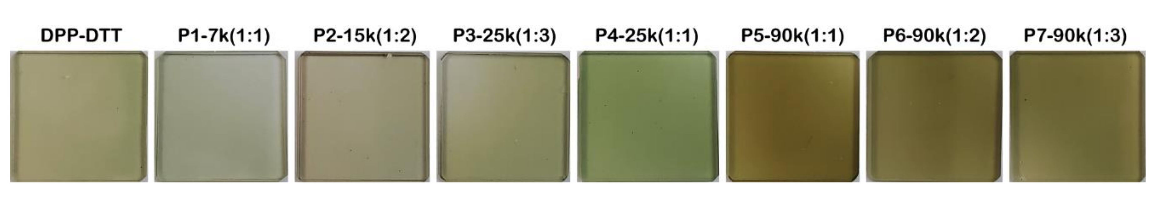
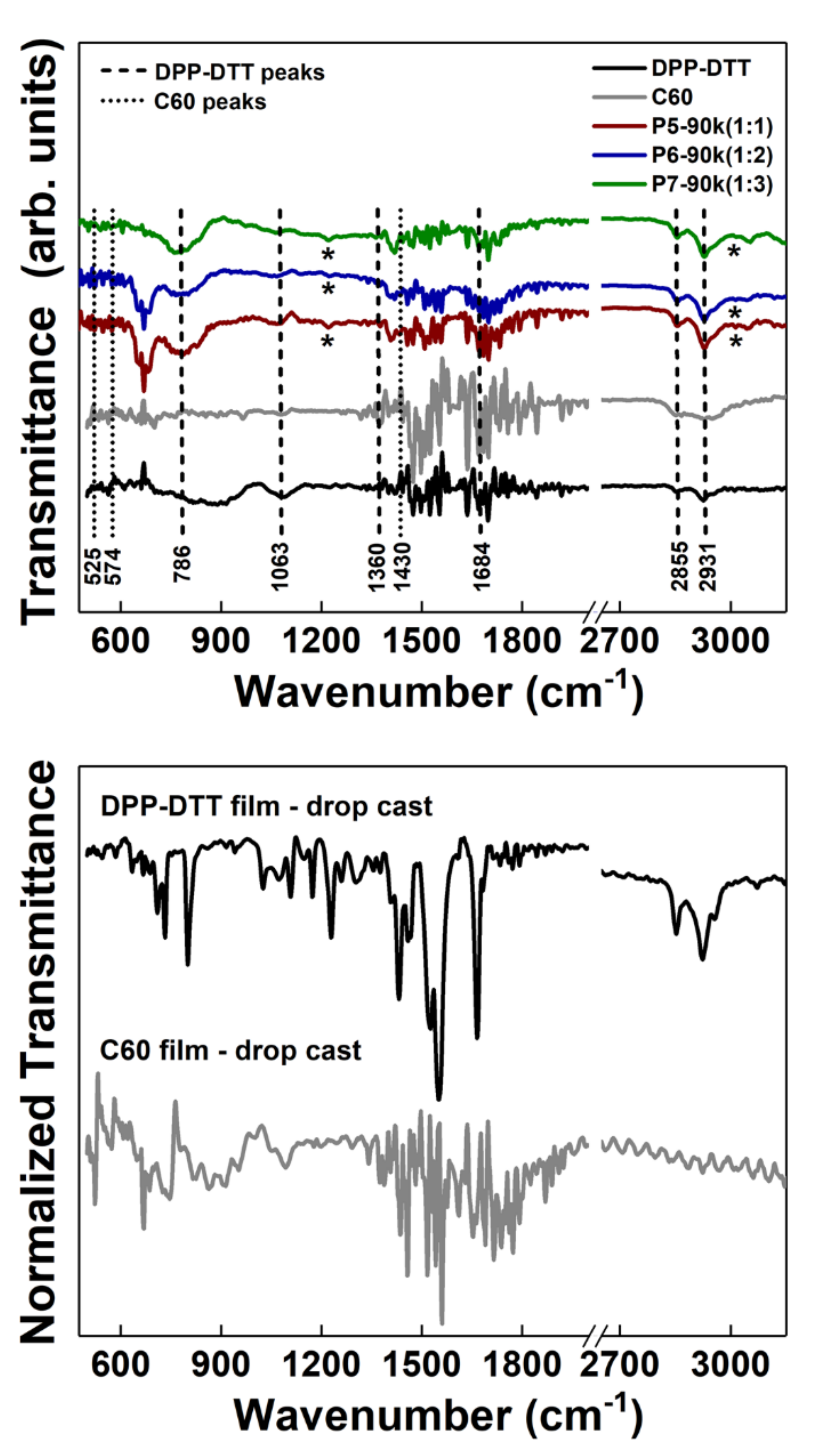
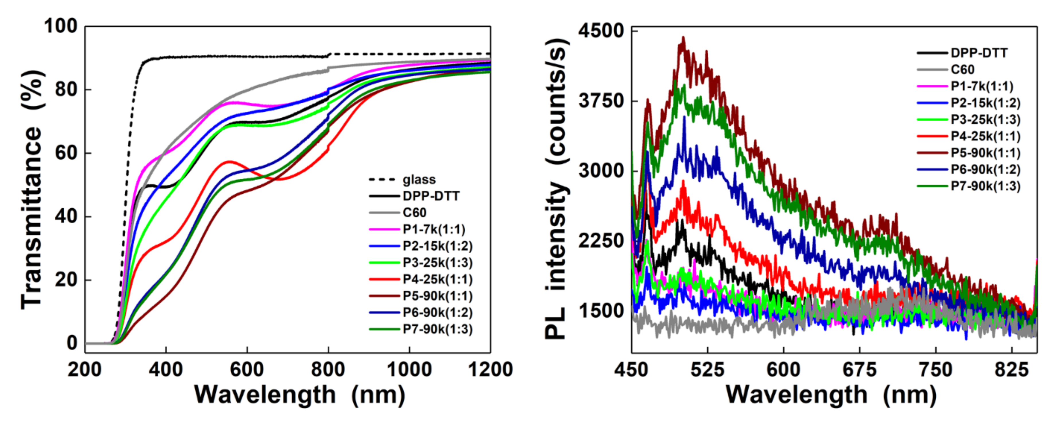
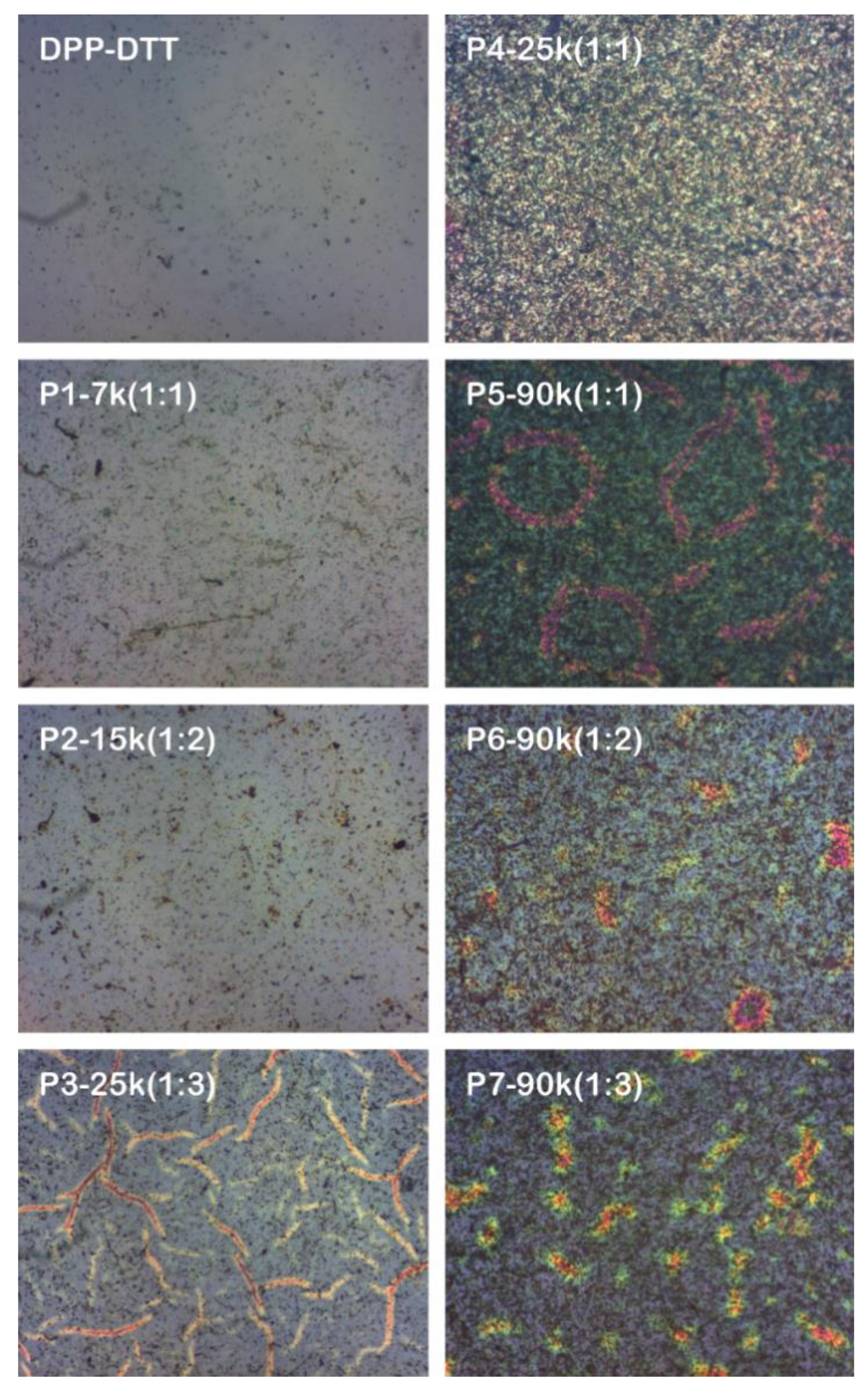
3. Results and Discussions
4. Conclusions
Author Contributions
Funding
Conflicts of Interest
References
- Gao, J.; Wang, J.; Xu, C.; Hu, Z.; Ma, X.; Zhang, X.; Niu, L.; Zhang, J.; Zhang, F. A critical review on efficient thick-film organic solar cells. Sol. RRL 2020, 4, 2000364. [Google Scholar] [CrossRef]
- Tonui, P.; Oseni, S.O.; Sharma, G.; Yan, Q.; Mola, G.T. Perovskites photovoltaic solar cells: An overview of current status. Renew. Sustain. Energy Rev. 2018, 91, 1025–1044. [Google Scholar] [CrossRef]
- Kang, A.K.; Zandi, M.H.; Gorji, N.E. Fabrication and degradation analysis of perovskite solar cells with graphene reduced oxide as hole transporting layer. J. Electron. Mater. 2020, 49, 2289–2295. [Google Scholar] [CrossRef]
- Berger, P.R.; Kim, M. Polymer solar cells: P3HT:PCBM and beyond. J. Renew. Sustain. Energy 2018, 10, 013508. [Google Scholar] [CrossRef]
- Zhang, G.; Fu, Y.; Xie, Z.; Zhang, Q. Synthesis of low bandgap polymer based on 3,6-dithien-2-yl-2,5-dialkylpyrrolo[3,4-c]pyrrole-1,4-dione for photovoltaic applications. Sol. Energy Mater. Sol. Cells 2011, 95, 1168–1173. [Google Scholar] [CrossRef]
- Singh, R.P.; Kushwaha, O.S. Polymer solar cells: An overview. Macromol. Symp. 2013, 327, 128–149. [Google Scholar] [CrossRef]
- Liu, Q.; Jiang, Y.; Jin, K.; Qin, J.; Xu, J.; Li, W.; Xiong, J.; Liu, J.; Xiao, Z.; Sun, K.; et al. 18% Efficiency organic solar cells. Sci. Bull. 2020, 65, 272–275. [Google Scholar] [CrossRef] [Green Version]
- Tsai, K.-H.; Huang, J.-S.; Liu, M.-Y.; Chao, C.-H.; Lee, C.-Y.; Hung, S.-C.; Lina, C.-F. High efficiency flexible polymer solar cells based on PET substrates with a nonannealing active layer. J. Electrochem. Soc. 2009, 156, B1188–B1191. [Google Scholar] [CrossRef]
- Lu, S.; Sun, Y.; Ren, K.; Liu, K.; Wang, Z.; Qu, S. Recent development in ITO-free flexible polymer solar cells. Polymers 2018, 10, 5. [Google Scholar] [CrossRef] [Green Version]
- Gao, Y.; Liu, M.; Zhang, Y.; Liu, Z.; Yang, Y.; Zhao, L. Recent Development on narrow bandgap conjugated polymers for polymer solar cells. Polymers 2017, 9, 39. [Google Scholar] [CrossRef] [Green Version]
- Jhuo, H.-J.; Yeh, P.-N.; Liao, S.-H.; Li, Y.-L.; Cheng, Y.-S.; Chen, S.-A. Review on the recent progress in low band gap conjugated polymers for bulk hetero-junction polymer solar cells. Chin. Chem. Soc. 2014, 61, 115–126. [Google Scholar] [CrossRef]
- He, Z.; Xiao, B.; Liu, F.; Wu, H.; Yang, Y.; Xiao, S.; Wang, C.; Russell, T.P.; Cao, Y. Single-junction polymer solar cells with high efficiency and photovoltage. Nat. Photonics 2015, 9, 174–179. [Google Scholar] [CrossRef]
- Li, J.; Zhao, Y.; Tan, H.S.; Guo, Y.; Di, C.-A.; Yu, G.; Liu, Y.; Lin, M.; Lim, S.H.; Zhou, Y.; et al. A stable solution-processed polymer semiconductor with record high-mobility for printed transistors. Sci. Rep. 2012, 2, 754. [Google Scholar] [CrossRef] [PubMed]
- Armin, A.; Hambsch, M.; Wolfer, P.; Jin, H.; Li, J.; Shi, Z.; Burn, P.L.; Meredith, P. Efficient, large area, and thick junction polymer solar cells with balanced mobilities and low defect densities. Adv. Energy Mater. 2014, 5, 1401221. [Google Scholar] [CrossRef]
- Liu, S.; You, P.; Li, J.; Li, J.; Lee, C.-S.; Ong, B.S.; Surya, C.; Yan, F. Enhanced efficiency in polymer solar cells by adding a high-mobility conjugated polymer. Energy Environ. Sci. 2015, 8, 1463–1470. [Google Scholar] [CrossRef]
- Li, W.; Hendriks, K.H.; Roelofs, W.S.; Kim, Y.; Wienk, M.M.; Janssen, R.A. Efficient small bandgap polymer solar cells with high fill factors for 300 nm thick films. Adv. Mater. 2013, 25, 3182–3186. [Google Scholar] [CrossRef]
- Xu, Y.; Huang, X.; Yuan, J.; Ma, W. From PCBM-polymer to low-cost and thermally stable C60/C70-polymer solar cells: The role of molecular structure, crystallinity, and morphology control. ACS Appl. Mater. Interfaces 2018, 10, 24037–24045. [Google Scholar] [CrossRef]
- Stanculescu, F.; Rasoga, O.; Catargiu, A.M.; Vacareanu, L.; Socol, M.; Breazu, C.; Preda, N.; Socol, G.; Stanculescu, A. MAPLE prepared heterostructures with arylene based polymer active layer for photovoltaic applications. Appl. Surf. Sci. 2015, 336, 240–248. [Google Scholar] [CrossRef]
- Huang, P.-H.; Wang, Y.-H.; Ke, J.-C.; Huang, C.-J. Investigation of various active layers for their performance on organic solar cells. Materials 2016, 9, 667. [Google Scholar] [CrossRef] [Green Version]
- Mozer, A.J.; Sariciftci, N.S. Conjugated polymer photovoltaic devices and materials. C. R. Chim. 2006, 9, 568–577. [Google Scholar] [CrossRef]
- Chen, J.-T.; Hsu, C.-S. Conjugated polymer nanostructures for organic solar cell applications. Polym. Chem. 2011, 2, 2707–2722. [Google Scholar] [CrossRef]
- Yu, G.; Gao, J.; Hummelen, J.C.; Wudi, F.; Heeger, A.J. Polymer photovoltaic cells: Enhanced efficiencies via a network of internal donor-acceptor heterojunctions. Science 1995, 270, 1789. [Google Scholar] [CrossRef] [Green Version]
- Anagnostou, K.; Stylianakis, M.M.; Petridis, K.; Kymakis, E. Building an organic solar cell: Fundamental procedures for device fabrication. Energies 2019, 12, 2188. [Google Scholar] [CrossRef] [Green Version]
- Cui, Y.; Yao, H.; Hong, L.; Zhang, T.; Tang, Y.; Lin, B.; Xian, K.; Gao, B.; An, C.; Bi, P.; et al. Organic photovoltaic cell with 17% efficiency and superior processability. Natl. Sci. Rev. 2020, 7, 1239–1246. [Google Scholar] [CrossRef]
- Armin, A.; Wolfer, P.; Shaw, P.E.; Hambsch, M.; Maasoumi, F.; Ullah, M.; Gann, E.; McNeill, C.R.; Li, J.; Shi, Z.; et al. Simultaneous enhancement of charge generation quantum yield and carrier transport in organic solar cells. J. Mater. Chem. C 2015, 41, 10799–10812. [Google Scholar] [CrossRef]
- Caricato, A.P.; Cesaria, M.; Gigli, G.; Loiudice, A.; Luches, A.; Martino, M.; Resta, V.; Rizzo, A.; Taurino, A. Poly-(3-hexylthiophene)/[6,6]-phenyl-C61-butyric-acid-methyl-ester bilayer deposition by matrix-assisted pulsed laser evaporation for organic photovoltaic applications. Appl. Phys. Lett. 2012, 100, 073306. [Google Scholar] [CrossRef]
- Socol, M.; Preda, N.; Stanculescu, A.; Breazu, C.; Florica, C.; Stanculescu, F.; Iftimie, S.; Girtan, M.; Popescu-Pelin, G.; Socol, G. Organic heterostructures deposited by MAPLE on AZO substrate. Appl. Surf. Sci. 2017, 417, 196–203. [Google Scholar] [CrossRef]
- Visan, A.; Cristescu, R.; Stefan, N.; Miroiu, M.; Nita, C.; Socol, M.; Florica, C.; Rasoga, O.; Zgura, I.; Sima, L.E.; et al. Antimicrobial polycaprolactone/polyethylene glycol embedded lysozyme coatings of Ti implants for osteoblast functional properties in tissue engineering. Appl. Surf. Sci. 2017, 417, 234–243. [Google Scholar] [CrossRef]
- Cristescu, R.; Mihaiescu, D.; Socol, G.; Stamatin, I.; Mihailescu, I.N.; Chrisey, D.B. Deposition of biopolymer thin films by matrix assisted pulsed laser evaporation. Appl. Phys. A 2004, 79, 1023–1026. [Google Scholar] [CrossRef]
- Rodrigo, K.; Czuba, P.; Toftmann, B.; Schou, J.; Pedrys, R. Surface morphology of polyethylene glycol films produced by matrix-assisted pulsed laser evaporation (MAPLE): Dependence on substrate temperature. Appl. Surf. Sci. 2006, 252, 4824–4828. [Google Scholar] [CrossRef]
- Leveugle, E.; Zhigilei, L.V. Molecular dynamics simulation study of the ejection and transport of polymer molecules in matrix-assisted pulsed laser evaporation. J. Appl. Phys. 2007, 102, 074914. [Google Scholar] [CrossRef] [Green Version]
- Sellinger, A.; Leveugle, E.; Fitz-Gerald, J.M.; Zhigilei, L.V. Generation of surface features in films deposited by matrix-assisted pulsed laser evaporation: The effects of the stress confinement and droplet landing velocity. Appl. Phys. A 2008, 92, 821–829. [Google Scholar] [CrossRef]
- Ausanio, G.; Califano, V.; Costantini, A.; Perretta, G.; Aronne, A.; Pepe, G.P.; Sannino, F.; Vicari, L.R.M. Matrix-assisted pulsed laser evaporation of β-glucosidase from a dopa/quinone target. Enzyme Microb. Technol. 2020, 132, 109414. [Google Scholar] [CrossRef]
- Yen, C.-P.; Yu, P.-F.; Wang, J.; Lin, J.-Y.; Chen, Y.-M.; Chen, S.-Y. Deposition of organic dyes for dye-sensitized solar cell by using matrix-assisted pulsed laser evaporation. AIP Adv. 2016, 6, 085011. [Google Scholar] [CrossRef] [Green Version]
- Socol, M.; Preda, N.; Rasoga, O.; Breazu, C.; Stavarache, I.; Stanculescu, F.; Socol, G.; Gherendi, F.; Grumezescu, V.; Stefan, N.; et al. Flexible heterostructures based on metal phthalocyanines thin films obtained by MAPLE. Appl. Surf. Sci. 2016, 374, 403–410. [Google Scholar] [CrossRef]
- Ge, W.; Li, N.K.; McCormick, R.D.; Lichtenberg, E.; Yingling, Y.G.; Stiff-Roberts, A.D. Emulsion-bBased RIR-MAPLE deposition of conjugated polymers: Primary solvent effect and its implications on organic solar cell performance. ACS Appl. Mater. Interfaces 2016, 8, 19494–19506. [Google Scholar] [CrossRef] [Green Version]
- Califano, V.; Bloisi, F.; Vicari, L.; Barra, M.; Cassinese, A.; Fanelli, E.; Buzio, R.; Valbusa, U.; Carella, A.; Roviello, A. Substrate temperature dependence of the structure of polythiophene thin films obtained by matrix assisted pulsed laser evaporation (MAPLE). Eur. Phys. J. Appl. Phys. 2009, 48, 10505. [Google Scholar] [CrossRef]
- Stanculescu, A.; Socol, G.; Vacareanu, L.; Socol, M.; Rasoga, O.; Breazu, C.; Girtan, M.; Stanculescu, F. MAPLE preparation and characterization of mixed arylenevinylene based oligomers:C60 layers. Appl. Surf. Sci. 2016, 374, 278–289. [Google Scholar] [CrossRef]
- Semenov, K.N.; Charykov, N.A.; Keskinov, V.A.; Piartman, A.K.; Blokhin, A.A.; Kopyrin, A.A. Solubility of light fullerenes in organic solvents. J. Chem. Eng. Data 2010, 55, 13–36. [Google Scholar] [CrossRef]
- Jelinek, M.; Kocourek, T.; Remsa, J.; Cristescu, R.; Mihailescu, I.N.; Chrisey, D.B. MAPLE applications in studying organic thin films. Laser Phys. 2007, 17, 66–70. [Google Scholar] [CrossRef]
- Zhang, Y.; Han, G.; Qin, M.; Shen, Y.; Lu, X.; Yi, Y.; Zhao, N. Spectroscopic study of charge transport at organic solid−water interface. Chem. Mater. 2018, 30, 5422–5428. [Google Scholar] [CrossRef]
- Yue, H.; Kong, L.; Wang, B.; Yuan, Q.; Zhang, Y.; Du, H.; Dong, Y.; Zhao, J. Synthesis and characterization of novel D-A type neutral blue electrochromic polymers containing Pyrrole[3-c]Pyrrole-1,4-Diketone as the acceptor units and the aromatics donor units with different planar structures. Polymers 2019, 11, 2023. [Google Scholar] [CrossRef] [PubMed] [Green Version]
- Pu, J.; Mo, Y.; Wan, S.; Wang, L. Fabrication of novel graphene–fullerene hybrid lubricating films based on self-assembly for MEMS applications. Chem. Commun. 2014, 50, 469–471. [Google Scholar] [CrossRef] [PubMed]
- Nishida, J.; Shigeto, S.; Yabumoto, S.; Hamaguchi, H. Anharmonic coupling of the CH-stretch and CH-bend vibrations of chloroform as studied by near-infrared electroabsorption spectroscopy. J. Chem. Phys. 2012, 137, 234501. [Google Scholar] [CrossRef]
- Leveugle, E.; Zhigilei, L.V.; Sellinger, A.; Fitz-Gerald, J.M.; Gogick, K.; Peman, G. Ejection of matrix-polymer clusters in matrix-assisted laser evaporation: Experimental observations. J. Phys. Conf. Ser. 2007, 59, 314–317. [Google Scholar] [CrossRef] [Green Version]
- Park, J.K.; Kim, C.; Walker, B.; Nguyen, T.-Q.; Seo, J.H. Morphology control of solution processable small molecule bulk heterojunction solar cells vi asolvent additives. RSC Adv. 2012, 2, 2232–2234. [Google Scholar] [CrossRef]
- Wang, X.; Zhu, Y.; Wang, G.; Qiua, L. Flexible and low-voltage phototransistor based on novel self-assembled phosphonic acids monolayers. Synth. Met. 2020, 269, 116563. [Google Scholar] [CrossRef]
- Armin, A.; Kassal, I.; Shaw, P.E.; Hambsch, M.; Stolterfoht, M.; Lyons, D.M.; Li, J.; Shi, Z.; Burn, P.L.; Meredith, P. Spectral dependence of the internal quantum efficiency of organic solar cells: Effect of charge generation pathways. J. Am. Chem. Soc. 2014, 136, 11465–11472. [Google Scholar] [CrossRef]
- Caricato, A.P.; Leggieri, G.; Martino, M.; Vantaggiato, A.; Valerini Cretì, D.A.; Lomascolo, M.; Manera, M.G.; Rella, R.; Anni, M. Dependence of the surface roughness of MAPLE-deposited films on the solvent parameters. Appl. Phys. A 2010, 101, 759–764. [Google Scholar] [CrossRef]
- Matus, M.; Kuzmany, H.; Sohmen, E. Self-trapped polaron exciton in neutral fullerene C60. Phys. Rev. Lett. 1992, 68, 2822–2825. [Google Scholar] [CrossRef]
- Xi, Y.; Wolf, C.M.; Pozzo, L.D. Self-assembly of donor–acceptor conjugated polymers induced by miscible ‘poor’ solvents. Soft Matter 2019, 15, 1799–1812. [Google Scholar] [CrossRef] [PubMed]
- Chaudhry, M.U.; Muhieddine, K.; Wawrzinek, R.; Li, J.; Lo, S.-C.; Namdas, E.B. Nano-alignment in semiconducting polymer films: A path to achieve high current density and brightness in organic light emitting transistors. ACS Photonics 2018, 5, 2137–2144. [Google Scholar] [CrossRef]
- Chen, L.; Pang, X.; Zhao, J. C60 tetragonal crystal sheet grown from evaporated C60 solution. New J. Chem. 2019, 43, 11524–11528. [Google Scholar] [CrossRef]
- Makhmanov, U.; Ismailova, O.; Kokhkharov, A.; Zakhidov, E.; Bakhramov, S. Features of self-aggregation of C60 molecules in toluene prepared by different methods. Phys. Lett. A 2016, 380, 2081–2084. [Google Scholar] [CrossRef]
- Yao, M.; Andersson, B.M.; Stenmark, P.; Sundqvist, B.; Liu, B.; Wågberg, T. Synthesis and growth mechanism of differently shaped C60 nano/microcrystals produced by evaporation of various aromatic C60 solutions. Carbon 2009, 47, 1181–1188. [Google Scholar] [CrossRef]
- Ding, Z.; Long, X.; Meng, B.; Bai, K.; Dou, C.; Liu, J.; Wang, L. Polymer solar cells with open-circuit voltage of 1.3 V using polymer electron acceptor with high LUMO level. Nano Energy 2017, 32, 216–224. [Google Scholar] [CrossRef]
- Elumalai, N.K.; Uddin, A. Open circuit voltage of organic solar cells: An in-depth review. Energy Environ. Sci. 2016, 9, 391–410. [Google Scholar] [CrossRef]
- Ulum, M.S.; Sesa, E.; Kasman; Belcher, W. The effect of active layer thickness on P3HT:PCBM nanoparticulate organic photovoltaic device performance. J. Phys. Conf. Ser. 2019, 1242, 012025.
- Gupta, D.; Mukhopadhyay, S.; Narayan, K.S. Fill factor in organic solar cells. Sol. Energy Mater. Sol. Cells 2010, 94, 1309–1313. [Google Scholar] [CrossRef]


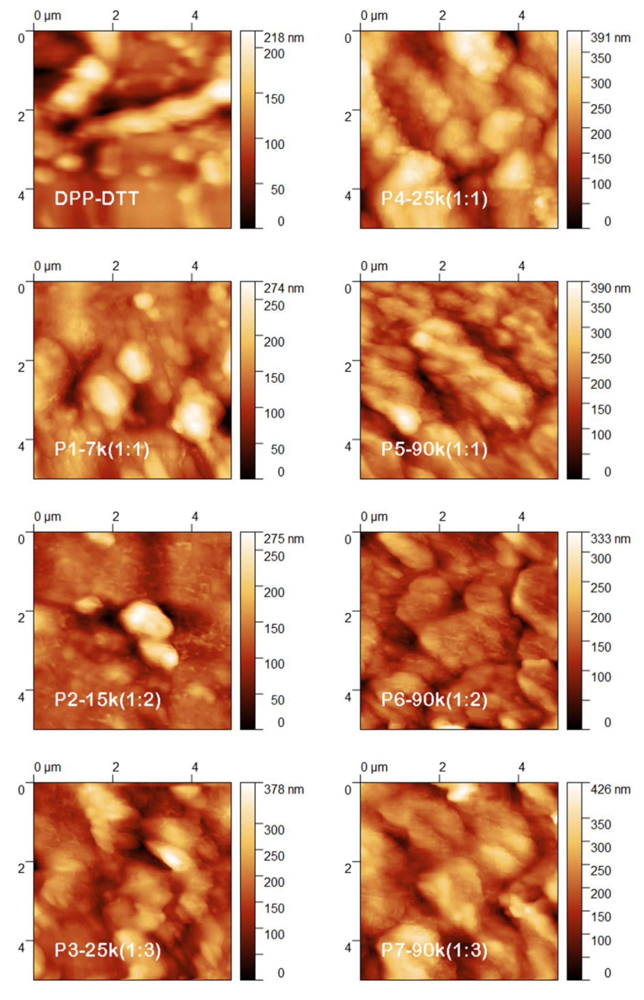
| Sample | Ratio | Number of the Laser Pulses | Thickness (nm) | RMS (nm) | Ra (nm) |
|---|---|---|---|---|---|
| DPP:DTT | - | 25 k | 35 | 27 | 21 |
| P1 | 1:1 | 7 k | 40 | 30 | 23 |
| P2 | 1:2 | 15 k | 40 | 35 | 24 |
| P3 | 1:3 | 25 k | 70 | 53 | 42 |
| P4 | 1:1 | 25 k | 70 | 64 | 52 |
| P5 | 1:1 | 90 k | 190 | 54 | 43 |
| P6 | 1:2 | 90 k | 160 | 61 | 46 |
| P7 | 1:3 | 90 k | 200 | 66 | 53 |
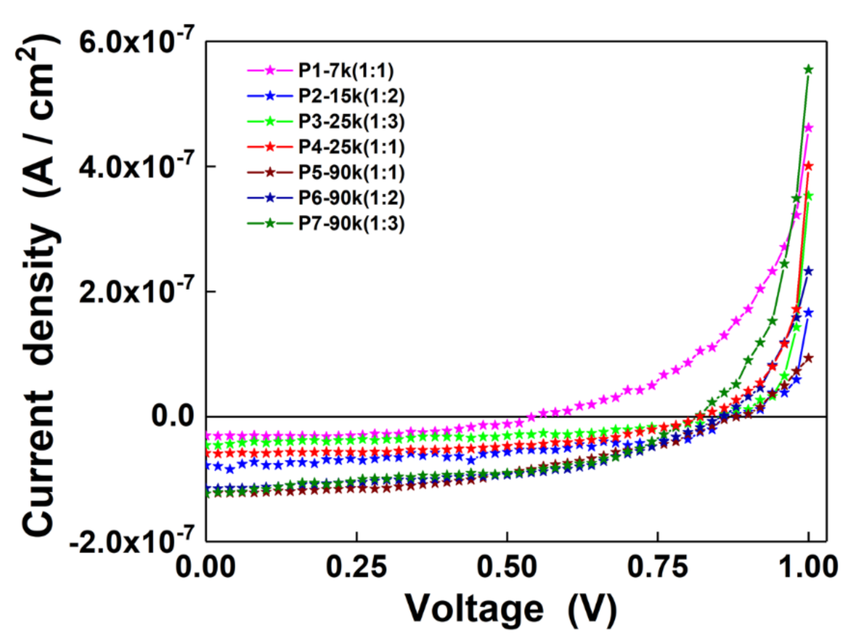
| Sample | VOC (V) | JSC (A/cm2) | Pmax (W) | FF |
|---|---|---|---|---|
| P1 | 0.54 | 3.0 × 10⁻⁸ | 8.8 × 10⁻⁹ | 0.54 |
| P2 | 0.86 | 7.8 × 10⁻⁸ | 2.9 × 10⁻⁸ | 0.43 |
| P3 | 0.86 | 4.7 × 10⁻⁸ | 1.7 × 10⁻⁸ | 0.42 |
| P4 | 0.82 | 5.9 × 10⁻⁸ | 2.5 × 10⁻⁸ | 0.52 |
| P5 | 0.88 | 1.2 × 10⁻⁷ | 4.6 × 10⁻⁸ | 0.44 |
| P6 | 0.86 | 1.1 × 10⁻⁷ | 5.0 × 10⁻⁸ | 0.53 |
| P7 | 0.82 | 1.2 × 10⁻⁷ | 4.7 × 10⁻⁸ | 0.48 |
Publisher’s Note: MDPI stays neutral with regard to jurisdictional claims in published maps and institutional affiliations. |
© 2020 by the authors. Licensee MDPI, Basel, Switzerland. This article is an open access article distributed under the terms and conditions of the Creative Commons Attribution (CC BY) license (http://creativecommons.org/licenses/by/4.0/).
Share and Cite
Socol, M.; Preda, N.; Breazu, C.; Costas, A.; Petre, G.; Stanculescu, A.; Popescu-Pelin, G.; Mihailescu, A.; Socol, G. Organic Thin Films Based on DPP-DTT:C60 Blends Deposited by MAPLE. Nanomaterials 2020, 10, 2366. https://doi.org/10.3390/nano10122366
Socol M, Preda N, Breazu C, Costas A, Petre G, Stanculescu A, Popescu-Pelin G, Mihailescu A, Socol G. Organic Thin Films Based on DPP-DTT:C60 Blends Deposited by MAPLE. Nanomaterials. 2020; 10(12):2366. https://doi.org/10.3390/nano10122366
Chicago/Turabian StyleSocol, Marcela, Nicoleta Preda, Carmen Breazu, Andreea Costas, Gabriela Petre, Anca Stanculescu, Gianina Popescu-Pelin, Andreea Mihailescu, and Gabriel Socol. 2020. "Organic Thin Films Based on DPP-DTT:C60 Blends Deposited by MAPLE" Nanomaterials 10, no. 12: 2366. https://doi.org/10.3390/nano10122366