
Two-Dimensional Semiconductor Optoelectronics Based on van der Waals Heterostructures


Abstract
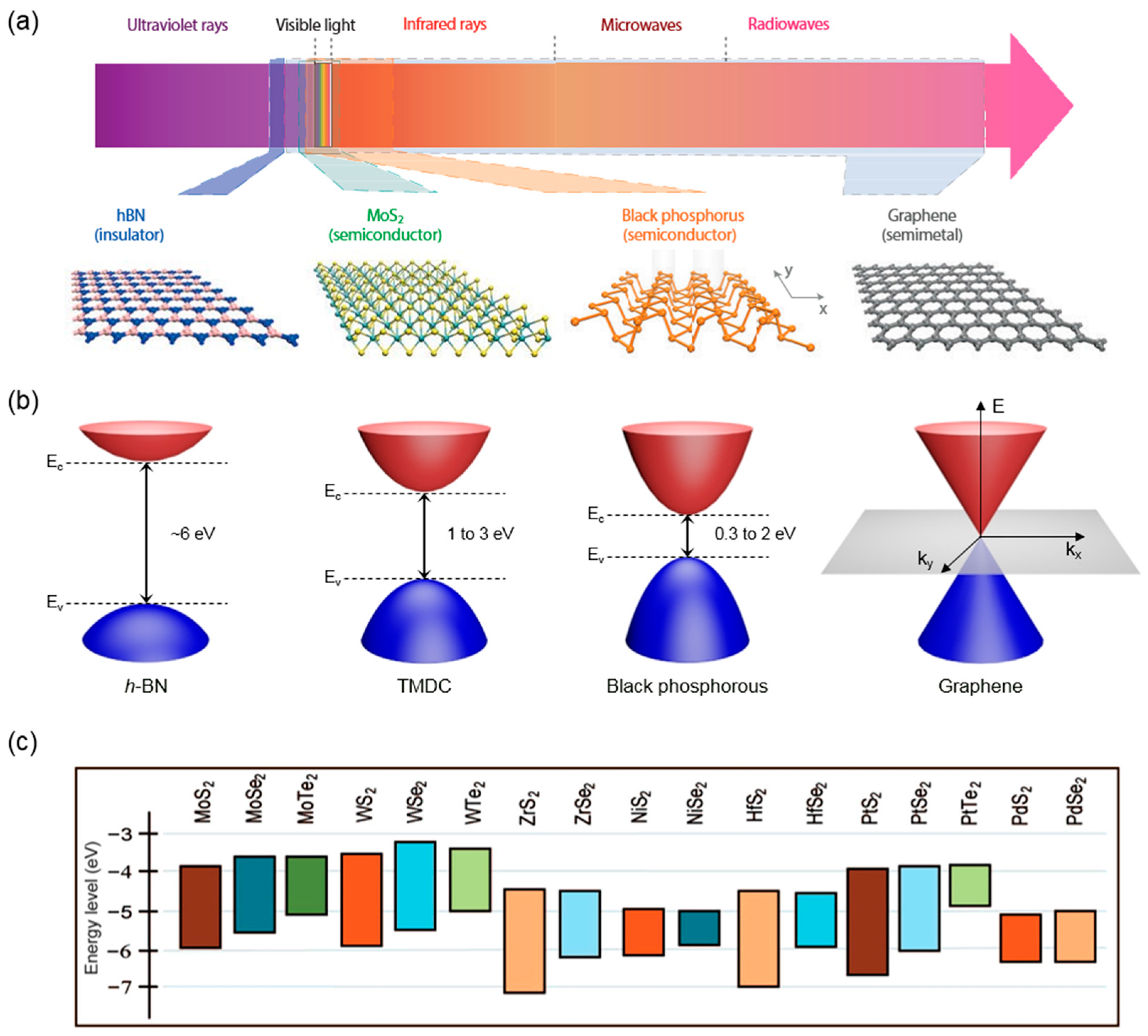
:1. Introduction
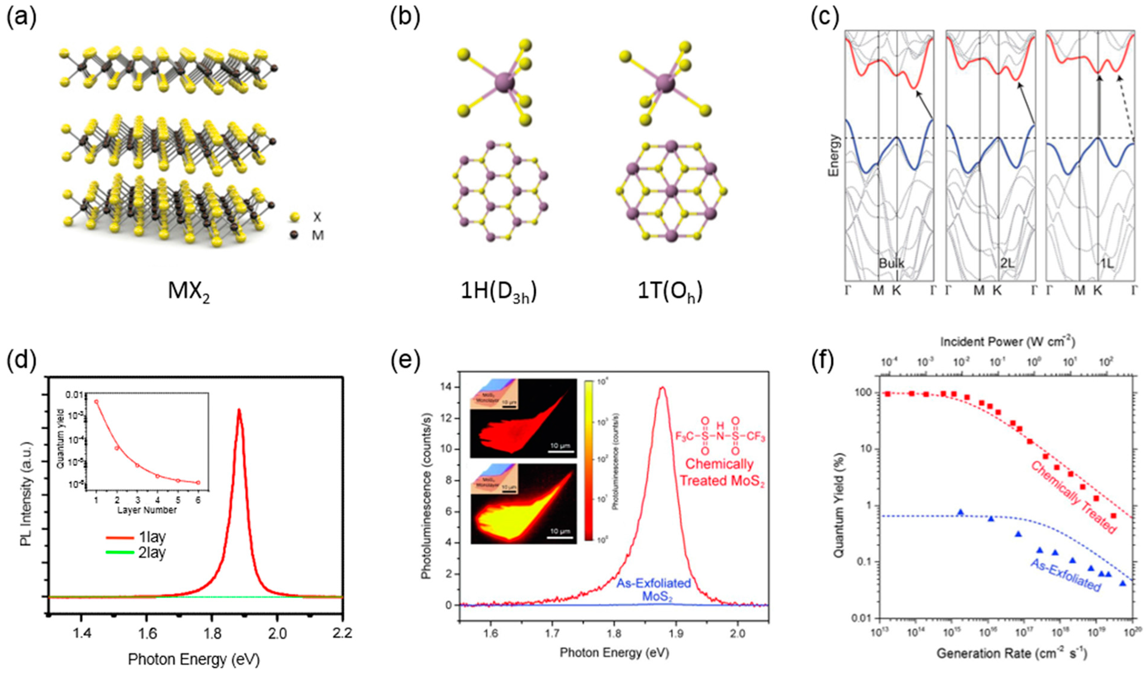
2. Transition Metal Dichalcogenides as 2D Semiconductors
3. Van der Waals Heterostructures Built from Various 2D Materials
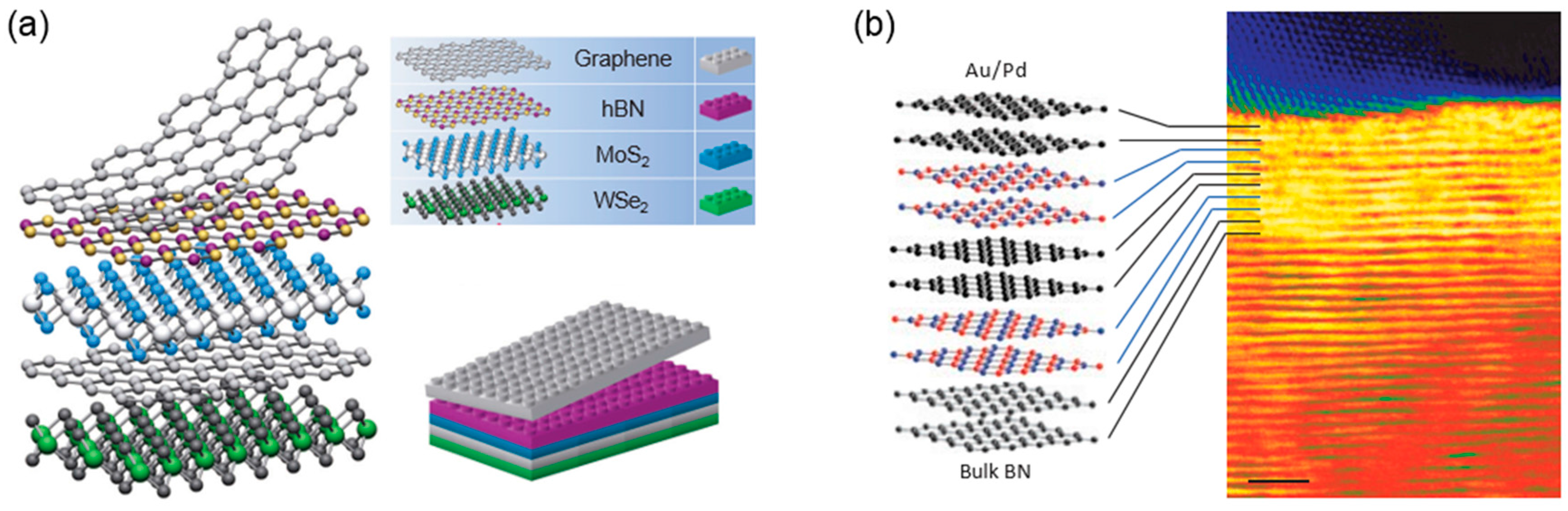
3.1. Features of 2D van der Waals Heterostructures
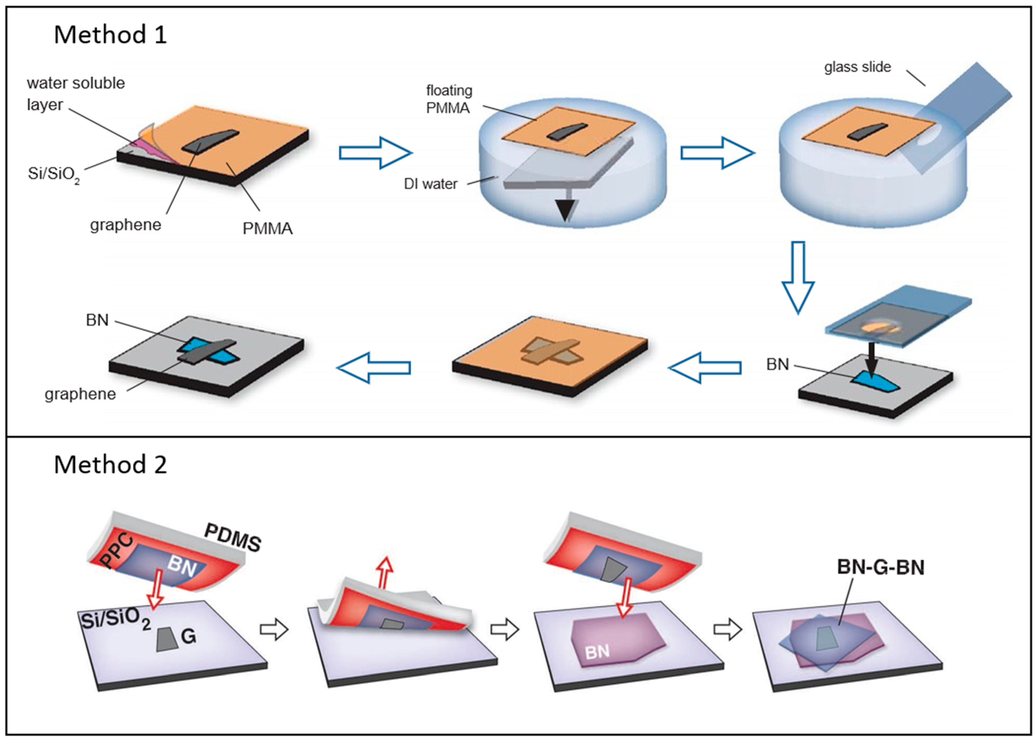
3.2. Fabrication of 2D van der Waals Heterostructures
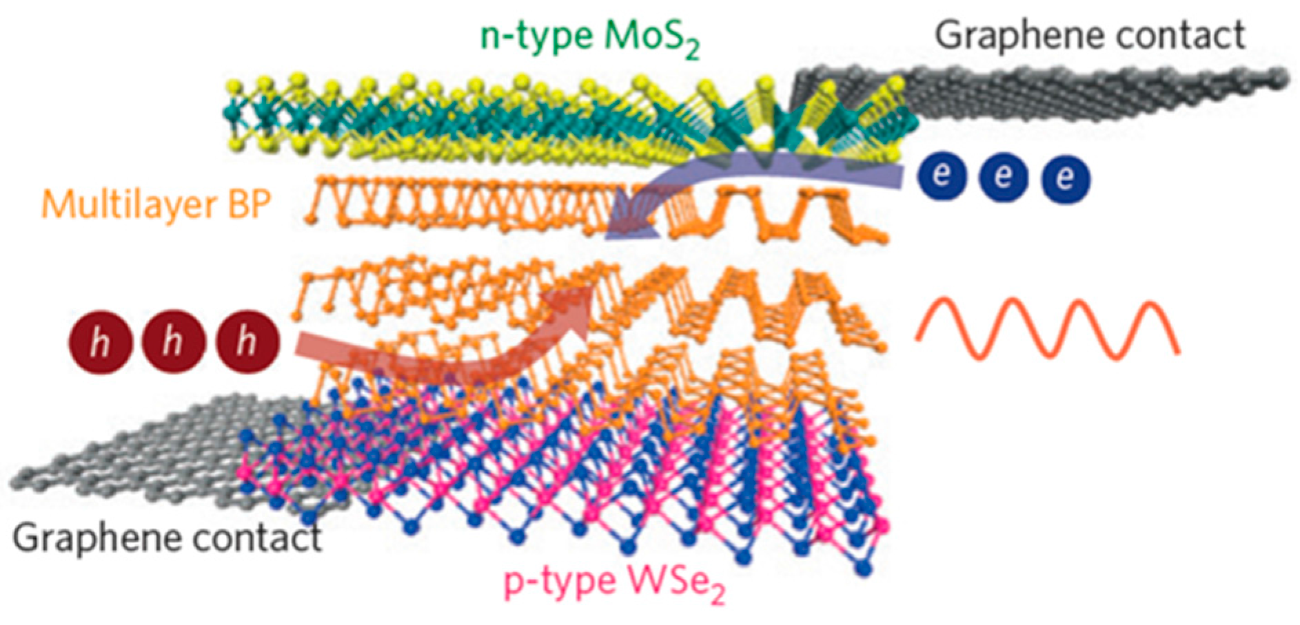
4. Optoelectronic Devices Based on 2D Semiconductor Heterostructures
4.1. Photodetection and Photovoltaic Devices
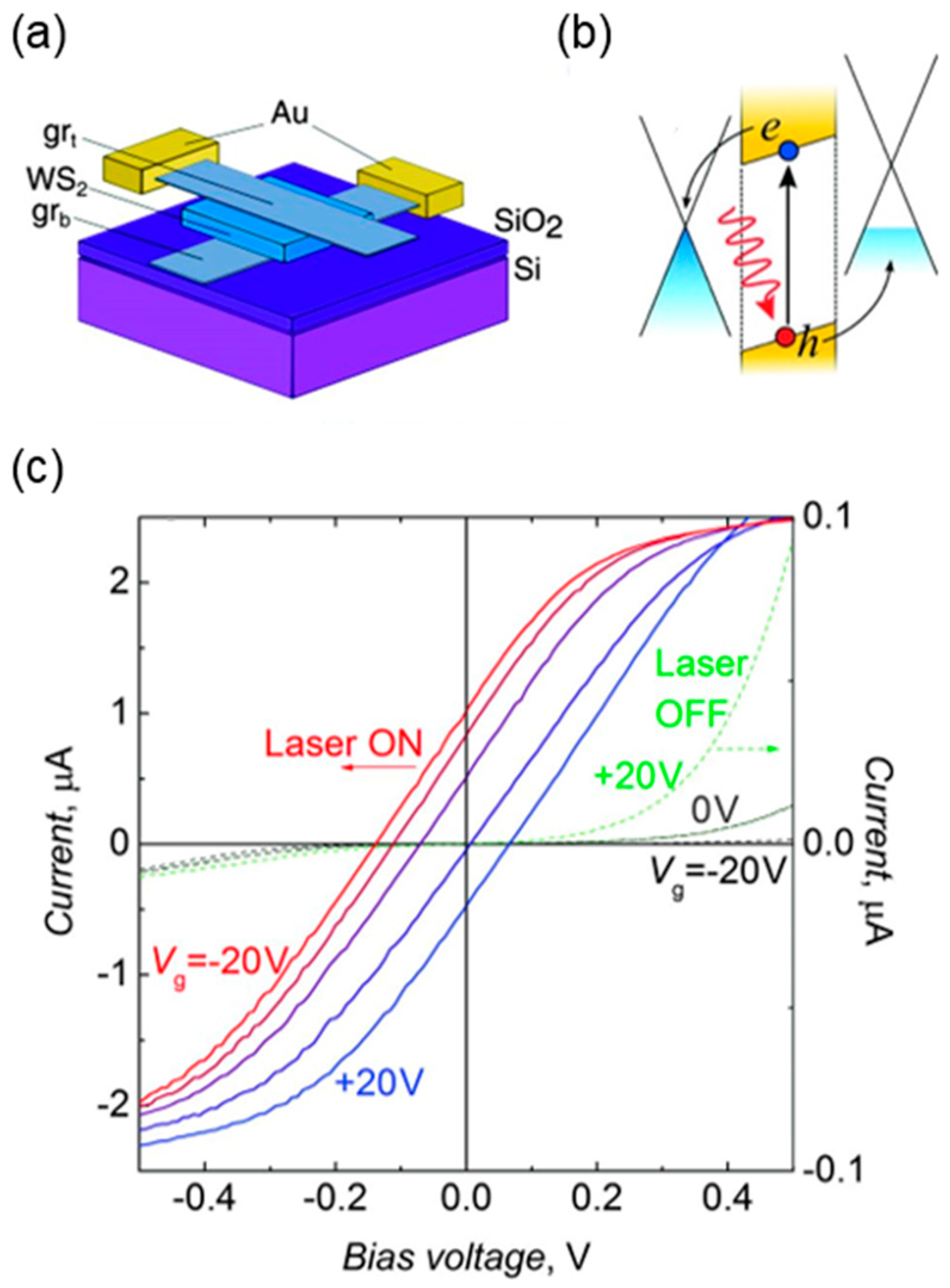
4.1.1. Photodetection Based on Graphene/TMDC/Graphene Heterostructures
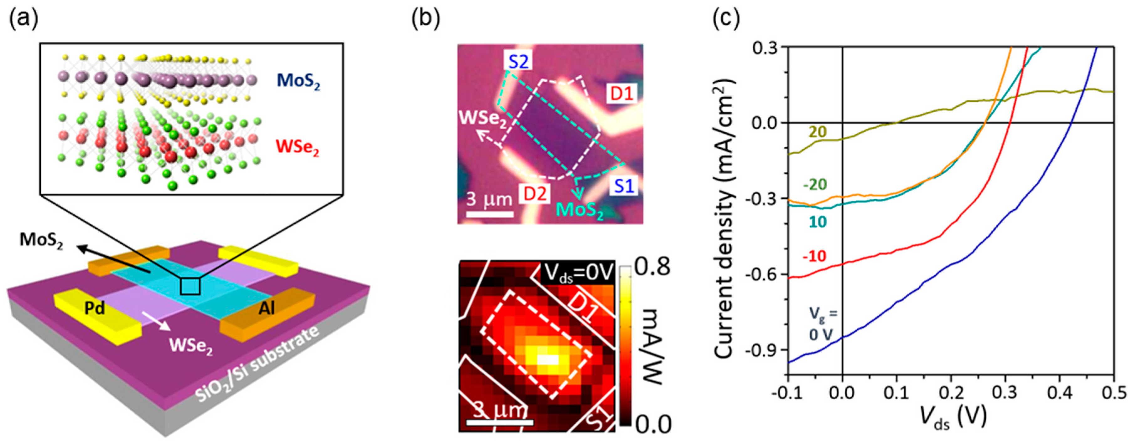
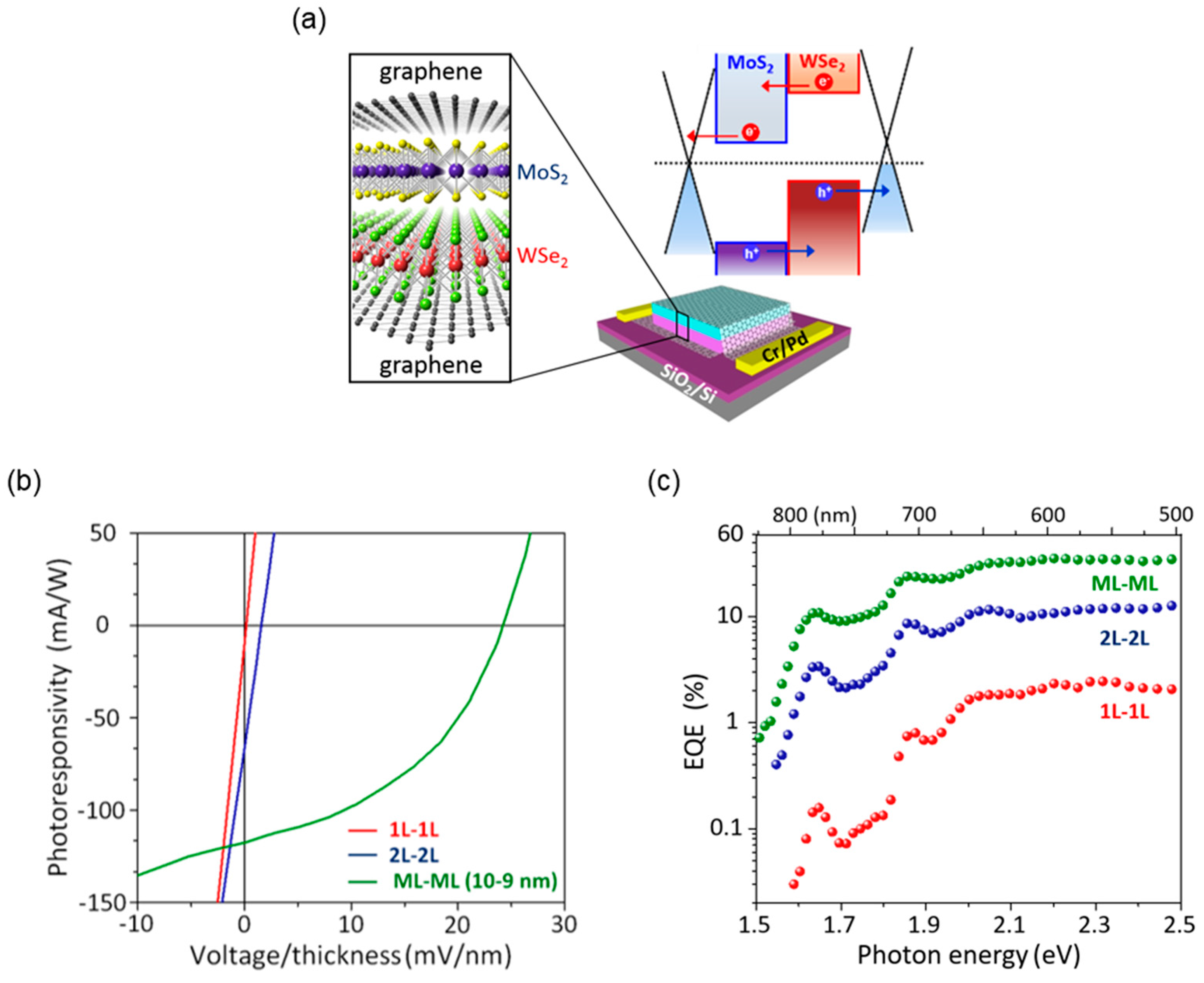
4.1.2. Atomically Thin p-n Heterojunctions Based on Semiconducting TMDCs
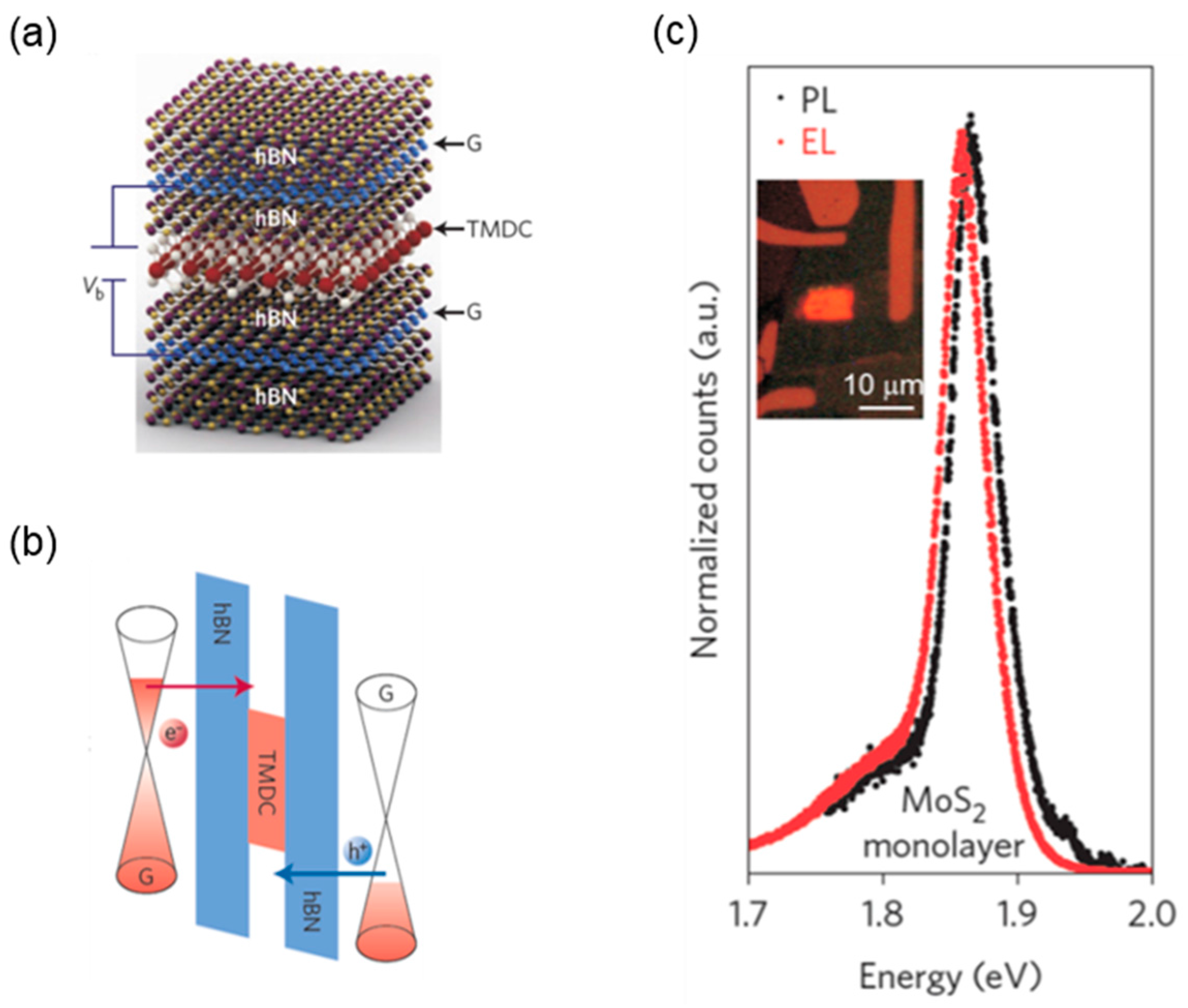
4.2. Light-Emitting Devices
5. Conclusions and Perspectives
Acknowledgments
Author Contributions
Conflicts of Interest
Abbreviations
| 2D | Two-dimensional |
| TMDCs | Transition metal dichalcogenides |
| FETs | Field-effect transistors |
| h-BN | Hexagonal boron nitride |
| vdW | van der Waals |
| PL | Photoluminescence |
| 3D | Three-dimensional |
| STEM | Scanning transmission electron microscopy |
| CVD | Chemical vapor deposition |
| LEDs | Light-emitting diodes |
| PMMA | Polymethyl methacrylate |
| PDMS | Polydimethylsiloxane |
| PPC | Polypropylene carbonate |
| EQE | External quantum efficiency |
| EL | Electroluminescence |
| MQWs | Multiple quantum wells |
References
- Novoselov, K.; Jiang, D.; Schedin, F.; Booth, T.; Khotkevich, V.; Morozov, S.; Geim, A. Two-dimensional atomic crystals. Proc. Natl. Acad. Sci. USA 2005, 102, 10451–10453. [Google Scholar] [CrossRef] [PubMed]
- Novoselov, K.S.; Fal’ko, V.I.; Colombo, L.; Gellert, P.R.; Schwab, M.G.; Kim, K. A roadmap for graphene. Nature 2012, 490, 192–200. [Google Scholar] [CrossRef] [PubMed]
- Xu, M.; Liang, T.; Shi, M.; Chen, H. Graphene-like two-dimensional materials. Chem. Rev. 2013, 113, 3766–3798. [Google Scholar] [CrossRef] [PubMed]
- Chhowalla, M.; Shin, H.S.; Eda, G.; Li, L.-J.; Loh, K.P.; Zhang, H. The chemistry of two-dimensional layered transition metal dichalcogenide nanosheets. Nat. Chem. 2013, 5, 263–275. [Google Scholar] [CrossRef] [PubMed]
- Osada, M.; Sasaki, T. Two-dimensional dielectric nanosheets: Novel nanoelectronics from nanocrystal building blocks. Adv. Mater. 2012, 24, 210–228. [Google Scholar] [CrossRef] [PubMed]
- Kalantar-zadeh, K.; Ou, J.Z.; Daeneke, T.; Strano, M.S.; Pumera, M.; Gras, S.L. Two-dimensional transition metal dichalcogenides in biosystems. Adv. Funct. Mater. 2015, 25, 5086–5099. [Google Scholar] [CrossRef]
- Jariwala, D.; Sangwan, V.K.; Lauhon, L.J.; Marks, T.J.; Hersam, M.C. Emerging device applications for semiconducting two-dimensional transition metal dichalcogenides. ACS Nano 2014, 8, 1102–1120. [Google Scholar] [CrossRef] [PubMed]
- Li, H.; Shi, Y.; Chiu, M.-H.; Li, L.-J. Emerging energy applications of two-dimensional layered transition metal dichalcogenides. Nano Energy 2015, 18, 293–305. [Google Scholar] [CrossRef]
- Duan, X.; Wang, C.; Pan, A.; Yu, R.; Duan, X. Two-dimensional transition metal dichalcogenides as atomically thin semiconductors: Opportunities and challenges. Chem. Soc. Rev. 2015, 44, 8859–8876. [Google Scholar] [CrossRef] [PubMed]
- Peng, B.; Ang, P.K.; Loh, K.P. Two-dimensional dichalcogenides for light-harvesting applications. Nano Today 2015, 10, 128–137. [Google Scholar] [CrossRef]
- Fiori, G.; Bonaccorso, F.; Iannaccone, G.; Palacios, T.; Neumaier, D.; Seabaugh, A.; Banerjee, S.K.; Colombo, L. Electronics based on two-dimensional materials. Nat. Nanotechnol. 2014, 9, 768–779. [Google Scholar] [CrossRef] [PubMed]
- Akinwande, D.; Petrone, N.; Hone, J. Two-dimensional flexible nanoelectronics. Nat. Commun. 2014, 5, 5678. [Google Scholar] [CrossRef] [PubMed]
- Wang, Q.H.; Kalantar-Zadeh, K.; Kis, A.; Coleman, J.N.; Strano, M.S. Electronics and optoelectronics of two-dimensional transition metal dichalcogenides. Nat. Nanotechnol. 2012, 7, 699–712. [Google Scholar] [CrossRef] [PubMed]
- Mak, K.F.; Shan, J. Photonics and optoelectronics of 2D semiconductor transition metal dichalcogenides. Nat. Photonics 2016, 10, 216–226. [Google Scholar] [CrossRef]
- Sun, Z.; Martinez, A.; Wang, F. Optical modulators with 2D layered materials. Nat. Photonics 2016, 10, 227–238. [Google Scholar] [CrossRef]
- Koppens, F.; Mueller, T.; Avouris, P.; Ferrari, A.; Vitiello, M.; Polini, M. Photodetectors based on graphene, other two-dimensional materials and hybrid systems. Nat. Nanotechnol. 2014, 9, 780–793. [Google Scholar] [CrossRef] [PubMed]
- Buscema, M.; Island, J.O.; Groenendijk, D.J.; Blanter, S.I.; Steele, G.A.; van der Zant, H.S.; Castellanos-Gomez, A. Photocurrent generation with two-dimensional van der Waals semiconductors. Chem. Soc. Rev. 2015, 44, 3691–3718. [Google Scholar] [CrossRef] [PubMed]
- Novoselov, K.S.; Geim, A.K.; Morozov, S.V.; Jiang, D.; Zhang, Y.; Dubonos, S.V.; Grigorieva, I.V.; Firsov, A.A. Electric field effect in atomically thin carbon films. Science 2004, 306, 666–669. [Google Scholar] [CrossRef] [PubMed]
- Zhang, Y.; Tan, Y.-W.; Stormer, H.L.; Kim, P. Experimental observation of the quantum Hall effect and Berry’s phase in graphene. Nature 2005, 438, 201–204. [Google Scholar] [CrossRef] [PubMed]
- Novoselov, K.; Geim, A.K.; Morozov, S.; Jiang, D.; Katsnelson, M.; Grigorieva, I.; Dubonos, S.; Firsov, A. Two-dimensional gas of massless Dirac fermions in graphene. Nature 2005, 438, 197–200. [Google Scholar] [CrossRef] [PubMed] [Green Version]
- Novoselov, K.S.; Jiang, Z.; Zhang, Y.; Morozov, S.; Stormer, H.; Zeitler, U.; Maan, J.; Boebinger, G.; Kim, P.; Geim, A. Room-temperature quantum Hall effect in graphene. Science 2007, 315, 1379–1379. [Google Scholar] [CrossRef] [PubMed] [Green Version]
- Lee, C.; Wei, X.; Kysar, J.W.; Hone, J. Measurement of the elastic properties and intrinsic strength of monolayer graphene. Science 2008, 321, 385–388. [Google Scholar] [CrossRef] [PubMed]
- Mak, K.F.; Lee, C.; Hone, J.; Shan, J.; Heinz, T.F. Atomically thin MoS2: A new direct-gap semiconductor. Phys. Rev. Lett. 2010, 105, 136805. [Google Scholar] [CrossRef] [PubMed]
- Ganatra, R.; Zhang, Q. Few-layer MoS2: A promising layered semiconductor. ACS Nano 2014, 8, 4074–4099. [Google Scholar] [CrossRef] [PubMed]
- Ling, X.; Wang, H.; Huang, S.; Xia, F.; Dresselhaus, M.S. The renaissance of black phosphorus. Proc. Natl. Acad. Sci. USA 2015, 112, 4523–4530. [Google Scholar] [CrossRef] [PubMed]
- Kang, J.; Tongay, S.; Zhou, J.; Li, J.; Wu, J. Band offsets and heterostructures of two-dimensional semiconductors. Appl. Phys. Lett. 2013, 102, 012111. [Google Scholar] [CrossRef]
- Xia, F.; Wang, H.; Xiao, D.; Dubey, M.; Ramasubramaniam, A. Two-dimensional material nanophotonics. Nat. Photonics 2014, 8, 899–907. [Google Scholar] [CrossRef]
- Rasmussen, F.A.; Thygesen, K.S. Computational 2D materials database: Electronic structure of transition-metal dichalcogenides and oxides. J. Phys. Chem. C 2015, 119, 13169–13183. [Google Scholar] [CrossRef] [Green Version]
- Radisavljevic, B.; Radenovic, A.; Brivio, J.; Giacometti, I.V.; Kis, A. Single-layer MoS2 transistors. Nat. Nanotechnol. 2011, 6, 147–150. [Google Scholar] [CrossRef] [PubMed]
- Roy, K.; Padmanabhan, M.; Goswami, S.; Sai, T.P.; Ramalingam, G.; Raghavan, S.; Ghosh, A. Graphene-MoS2 hybrid structures for multifunctional photoresponsive memory devices. Nat. Nanotechnol. 2013, 8, 826–830. [Google Scholar] [CrossRef] [PubMed]
- Choi, M.S.; Lee, G.-H.; Yu, Y.-J.; Lee, D.-Y.; Lee, S.H.; Kim, P.; Hone, J.; Yoo, W.J. Controlled charge trapping by molybdenum disulphide and graphene in ultrathin heterostructured memory devices. Nat. Commun. 2013, 4, 1624. [Google Scholar] [CrossRef] [PubMed]
- Bertolazzi, S.; Krasnozhon, D.; Kis, A. Nonvolatile memory cells based on MoS2/graphene heterostructures. ACS Nano 2013, 7, 3246–3252. [Google Scholar] [CrossRef] [PubMed]
- Cheiwchanchamnangij, T.; Lambrecht, W.R. Quasiparticle band structure calculation of monolayer, bilayer, and bulk MoS2. Phys. Rev. B 2012, 85, 205302. [Google Scholar] [CrossRef]
- Mak, K.F.; He, K.; Shan, J.; Heinz, T.F. Control of valley polarization in monolayer MoS2 by optical helicity. Nat. Nanotechnol. 2012, 7, 494–498. [Google Scholar] [CrossRef] [PubMed]
- Zeng, H.; Dai, J.; Yao, W.; Xiao, D.; Cui, X. Valley polarization in MoS2 monolayers by optical pumping. Nat. Nanotechnol. 2012, 7, 490–493. [Google Scholar] [CrossRef] [PubMed]
- Sie, E.J.; McIver, J.W.; Lee, Y.-H.; Fu, L.; Kong, J.; Gedik, N. Valley-selective optical Stark effect in monolayer WS2. Nat. Mater. 2015, 14, 290–294. [Google Scholar] [CrossRef] [PubMed]
- Britnell, L.; Ribeiro, R.; Eckmann, A.; Jalil, R.; Belle, B.; Mishchenko, A.; Kim, Y.-J.; Gorbachev, R.; Georgiou, T.; Morozov, S. Strong light-matter interactions in heterostructures of atomically thin films. Science 2013, 340, 1311–1314. [Google Scholar] [CrossRef] [PubMed]
- Fang, H.; Battaglia, C.; Carraro, C.; Nemsak, S.; Ozdol, B.; Kang, J.S.; Bechtel, H.A.; Desai, S.B.; Kronast, F.; Unal, A.A.; et al. Strong interlayer coupling in van der Waals heterostructures built from single-layer chalcogenides. Proc. Natl. Acad. Sci. USA 2014, 111, 6198–6202. [Google Scholar] [CrossRef] [PubMed]
- Liu, X.; Galfsky, T.; Sun, Z.; Xia, F.; Lin, E.-C.; Lee, Y.-H.; Kéna-Cohen, S.; Menon, V.M. Strong light–matter coupling in two-dimensional atomic crystals. Nat. Photonics 2015, 9, 30–34. [Google Scholar] [CrossRef]
- Ramasubramaniam, A. Large excitonic effects in monolayers of molybdenum and tungsten dichalcogenides. Phys. Rev. B 2012, 86, 115409. [Google Scholar] [CrossRef]
- Komsa, H.-P.; Krasheninnikov, A.V. Effects of confinement and environment on the electronic structure and exciton binding energy of MoS2 from first principles. Phys. Rev. B 2012, 86, 241201. [Google Scholar] [CrossRef]
- Ugeda, M.M.; Bradley, A.J.; Shi, S.-F.; Felipe, H.; Zhang, Y.; Qiu, D.Y.; Ruan, W.; Mo, S.-K.; Hussain, Z.; Shen, Z.-X.; et al. Giant bandgap renormalization and excitonic effects in a monolayer transition metal dichalcogenide semiconductor. Nat. Mater. 2014, 13, 1091–1095. [Google Scholar] [CrossRef] [PubMed]
- Chernikov, A.; Berkelbach, T.C.; Hill, H.M.; Rigosi, A.; Li, Y.; Aslan, O.B.; Reichman, D.R.; Hybertsen, M.S.; Heinz, T.F. Exciton binding energy and nonhydrogenic Rydberg series in monolayer WS2. Phys. Rev. Lett. 2014, 113, 076802. [Google Scholar] [CrossRef] [PubMed]
- Li, L.; Yu, Y.; Ye, G.J.; Ge, Q.; Ou, X.; Wu, H.; Feng, D.; Chen, X.H.; Zhang, Y. Black phosphorus field-effect transistors. Nat. Nanotechnol. 2014, 9, 372–377. [Google Scholar] [CrossRef] [PubMed]
- Tran, V.; Soklaski, R.; Liang, Y.; Yang, L. Layer-controlled band gap and anisotropic excitons in few-layer black phosphorus. Phys. Rev. B 2014, 89, 235319. [Google Scholar] [CrossRef]
- Xia, F.; Wang, H.; Jia, Y. Rediscovering black phosphorus as an anisotropic layered material for optoelectronics and electronics. Nat. Commun. 2014, 5, 4458. [Google Scholar] [CrossRef] [PubMed]
- Dean, C.R.; Young, A.F.; Meric, I.; Lee, C.; Wang, L.; Sorgenfrei, S.; Watanabe, K.; Taniguchi, T.; Kim, P.; Shepard, K.; et al. Boron nitride substrates for high-quality graphene electronics. Nat. Nanotechnol. 2010, 5, 722–726. [Google Scholar] [CrossRef] [PubMed]
- Lee, G.-H.; Yu, Y.-J.; Cui, X.; Petrone, N.; Lee, C.-H.; Choi, M.S.; Lee, D.-Y.; Lee, C.; Yoo, W.J.; Watanabe, K.; et al. Flexible and transparent MoS2 field-effect transistors on hexagonal boron nitride-graphene heterostructures. ACS Nano 2013, 7, 7931–7936. [Google Scholar] [CrossRef] [PubMed]
- Cui, X.; Lee, G.-H.; Kim, Y.D.; Arefe, G.; Huang, P.Y.; Lee, C.-H.; Chenet, D.A.; Zhang, X.; Wang, L.; Ye, F.; et al. Multi-terminal transport measurements of MoS2 using a van der Waals heterostructure device platform. Nat. Nanotechnol. 2015, 10, 534–540. [Google Scholar] [CrossRef] [PubMed]
- Dean, C.; Young, A.; Wang, L.; Meric, I.; Lee, G.-H.; Watanabe, K.; Taniguchi, T.; Shepard, K.; Kim, P.; Hone, J. Graphene based heterostructures. Solid State Commun. 2012, 152, 1275–1282. [Google Scholar] [CrossRef]
- Geim, A.K.; Grigorieva, I.V. Van der Waals heterostructures. Nature 2013, 499, 419–425. [Google Scholar] [CrossRef] [PubMed]
- Novoselov, K.; Mishchenko, A.; Carvalho, A.; Neto, A.C. 2D materials and van der Waals heterostructures. Science 2016, 353. [Google Scholar] [CrossRef] [PubMed]
- Lee, G.-H.; Lee, C.-H.; van der Zande, A.M.; Han, M.; Cui, X.; Arefe, G.; Nuckolls, C.; Heinz, T.F.; Hone, J.; Kim, P. Heterostructures based on inorganic and organic van der Waals systems. APL Mater. 2014, 2, 092511. [Google Scholar] [CrossRef]
- Kappera, R.; Voiry, D.; Yalcin, S.E.; Branch, B.; Gupta, G.; Mohite, A.D.; Chhowalla, M. Phase-engineered low-resistance contacts for ultrathin MoS2 transistors. Nat. Mater. 2014, 13, 1128–1134. [Google Scholar] [CrossRef] [PubMed]
- Schmidt, H.; Giustiniano, F.; Eda, G. Electronic transport properties of transition metal dichalcogenide field-effect devices: Surface and interface effects. Chem. Soc. Rev. 2015, 44, 7715–7736. [Google Scholar] [CrossRef] [PubMed]
- Splendiani, A.; Sun, L.; Zhang, Y.; Li, T.; Kim, J.; Chim, C.-Y.; Galli, G.; Wang, F. Emerging photoluminescence in monolayer MoS2. Nano Lett. 2010, 10, 1271–1275. [Google Scholar] [CrossRef] [PubMed]
- Eda, G.; Yamaguchi, H.; Voiry, D.; Fujita, T.; Chen, M.; Chhowalla, M. Photoluminescence from chemically exfoliated MoS2. Nano Lett. 2011, 11, 5111–5116. [Google Scholar] [CrossRef] [PubMed]
- Wang, H.; Zhang, C.; Rana, F. Ultrafast dynamics of defect-assisted electron–hole recombination in monolayer MoS2. Nano Lett. 2014, 15, 339–345. [Google Scholar] [CrossRef] [PubMed]
- Yuan, L.; Huang, L. Exciton dynamics and annihilation in WS2 2D semiconductors. Nanoscale 2015, 7, 7402–7408. [Google Scholar] [CrossRef] [PubMed]
- Mouri, S.; Miyauchi, Y.; Matsuda, K. Tunable photoluminescence of monolayer MoS2 via chemical doping. Nano Lett. 2013, 13, 5944–5948. [Google Scholar] [CrossRef] [PubMed]
- Wei, X.; Yu, Z.; Hu, F.; Cheng, Y.; Yu, L.; Wang, X.; Xiao, M.; Wang, J.; Wang, X.; Shi, Y. Mo-O bond doping and related-defect assisted enhancement of photoluminescence in monolayer MoS2. AIP Adv. 2014, 4, 123004. [Google Scholar] [CrossRef]
- Amani, M.; Lien, D.-H.; Kiriya, D.; Xiao, J.; Azcatl, A.; Noh, J.; Madhvapathy, S.R.; Addou, R.; Santosh, K.; Dubey, M.; et al. Near-unity photoluminescence quantum yield in MoS2. Science 2015, 350, 1065–1068. [Google Scholar] [CrossRef] [PubMed]
- Amani, M.; Burke, R.A.; Ji, X.; Zhao, P.; Lien, D.-H.; Taheri, P.; Ahn, G.H.; Kiriya, D.; Ager, J.W.; Yablonovitch, E.; et al. High luminescence efficiency in MoS2 grown by chemical vapor deposition. ACS Nano 2016, 10, 6535–6541. [Google Scholar] [CrossRef] [PubMed]
- Carvalho, A.; Ribeiro, R.; Neto, A.C. Band nesting and the optical response of two-dimensional semiconducting transition metal dichalcogenides. Phys. Rev. B 2013, 88, 115205. [Google Scholar] [CrossRef]
- Bernardi, M.; Palummo, M.; Grossman, J.C. Extraordinary sunlight absorption and one nanometer thick photovoltaics using two-dimensional monolayer materials. Nano Lett. 2013, 13, 3664–3670. [Google Scholar] [CrossRef] [PubMed]
- Arora, A.; Koperski, M.; Nogajewski, K.; Marcus, J.; Faugeras, C.; Potemski, M. Excitonic resonances in thin films of WSe2: From monolayer to bulk material. Nanoscale 2015, 7, 10421–10429. [Google Scholar] [CrossRef] [PubMed]
- Mak, K.F.; He, K.; Lee, C.; Lee, G.H.; Hone, J.; Heinz, T.F.; Shan, J. Tightly bound trions in monolayer MoS2. Nat. Mater. 2013, 12, 207–211. [Google Scholar] [CrossRef] [PubMed]
- Wang, X.; Xia, F. Van der Waals heterostructures: Stacked 2D materials shed light. Nat. Mater. 2015, 14, 264–265. [Google Scholar] [CrossRef] [PubMed]
- Roy, T.; Tosun, M.; Kang, J.S.; Sachid, A.B.; Desai, S.B.; Hettick, M.; Hu, C.C.; Javey, A. Field-effect transistors built from all two-dimensional material components. ACS Nano 2014, 8, 6259–6264. [Google Scholar] [CrossRef] [PubMed]
- Haigh, S.; Gholinia, A.; Jalil, R.; Romani, S.; Britnell, L.; Elias, D.; Novoselov, K.; Ponomarenko, L.; Geim, A.; Gorbachev, R. Cross-sectional imaging of individual layers and buried interfaces of graphene-based heterostructures and superlattices. Nat. Mater. 2012, 11, 764–767. [Google Scholar] [CrossRef] [PubMed]
- Dean, C.; Young, A.; Cadden-Zimansky, P.; Wang, L.; Ren, H.; Watanabe, K.; Taniguchi, T.; Kim, P.; Hone, J.; Shepard, K. Multicomponent fractional quantum Hall effect in graphene. Nat. Phys. 2011, 7, 693–696. [Google Scholar] [CrossRef]
- Dean, C.; Wang, L.; Maher, P.; Forsythe, C.; Ghahari, F.; Gao, Y.; Katoch, J.; Ishigami, M.; Moon, P.; Koshino, M.; et al. Hofstadter’s butterfly and the fractal quantum Hall effect in moire superlattices. Nature 2013, 497, 598–602. [Google Scholar] [PubMed]
- Britnell, L.; Gorbachev, R.; Geim, A.; Ponomarenko, L.; Mishchenko, A.; Greenaway, M.; Fromhold, T.; Novoselov, K.; Eaves, L. Resonant tunnelling and negative differential conductance in graphene transistors. Nat. Commun. 2013, 4, 1794. [Google Scholar] [CrossRef] [PubMed]
- Lin, Y.-C.; Ghosh, R.K.; Addou, R.; Lu, N.; Eichfeld, S.M.; Zhu, H.; Li, M.-Y.; Peng, X.; Kim, M.J.; Li, L.-J.; et al. Atomically thin resonant tunnel diodes built from synthetic van der Waals heterostructures. Nat. Commun. 2015, 6, 7311. [Google Scholar] [CrossRef] [PubMed]
- Gorbachev, R.; Geim, A.; Katsnelson, M.; Novoselov, K.; Tudorovskiy, T.; Grigorieva, I.; MacDonald, A.; Morozov, S.; Watanabe, K.; Taniguchi, T. Strong Coulomb drag and broken symmetry in double-layer graphene. Nat. Phys. 2012, 8, 896–901. [Google Scholar] [CrossRef] [Green Version]
- Britnell, L.; Gorbachev, R.; Jalil, R.; Belle, B.; Schedin, F.; Mishchenko, A.; Georgiou, T.; Katsnelson, M.; Eaves, L.; Morozov, S.; et al. Field-effect tunneling transistor based on vertical graphene heterostructures. Science 2012, 335, 947–950. [Google Scholar] [CrossRef] [PubMed] [Green Version]
- Georgiou, T.; Jalil, R.; Belle, B.D.; Britnell, L.; Gorbachev, R.V.; Morozov, S.V.; Kim, Y.-J.; Gholinia, A.; Haigh, S.J.; Makarovsky, O.; et al. Vertical field-effect transistor based on graphene-WS2 heterostructures for flexible and transparent electronics. Nat. Nanotechnol. 2013, 8, 100–103. [Google Scholar] [CrossRef] [PubMed]
- Hong, X.; Kim, J.; Shi, S.-F.; Zhang, Y.; Jin, C.; Sun, Y.; Tongay, S.; Wu, J.; Zhang, Y.; Wang, F. Ultrafast charge transfer in atomically thin MoS2/WS2 heterostructures. Nat. Nanotechnol. 2014, 9, 682–686. [Google Scholar] [CrossRef] [PubMed]
- Wang, H.; Zhang, C.; Chan, W.; Tiwari, S.; Rana, F. Ultrafast response of monolayer molybdenum disulfide photodetectors. Nat. Commun. 2015, 6, 8831. [Google Scholar] [CrossRef] [PubMed]
- Massicotte, M.; Schmidt, P.; Vialla, F.; Schädler, K.; Reserbat-Plantey, A.; Watanabe, K.; Taniguchi, T.; Tielrooij, K.; Koppens, F. Picosecond photoresponse in van der Waals heterostructures. Nat. Nanotechnol. 2016, 11, 42–46. [Google Scholar] [CrossRef] [PubMed]
- Cheng, R.; Li, D.; Zhou, H.; Wang, C.; Yin, A.; Jiang, S.; Liu, Y.; Chen, Y.; Huang, Y.; Duan, X. Electroluminescence and photocurrent generation from atomically sharp WSe2/MoS2 heterojunction p-n diodes. Nano Lett. 2014, 14, 5590–5597. [Google Scholar] [CrossRef] [PubMed]
- Withers, F.; Del Pozo-Zamudio, O.; Mishchenko, A.; Rooney, A.; Gholinia, A.; Watanabe, K.; Taniguchi, T.; Haigh, S.; Geim, A.; Tartakovskii, A.; et al. Light-emitting diodes by band-structure engineering in van der Waals heterostructures. Nat. Mater. 2015, 14, 301–306. [Google Scholar] [CrossRef] [PubMed]
- Withers, F.; Del Pozo-Zamudio, O.; Schwarz, S.; Dufferwiel, S.; Walker, P.; Godde, T.; Rooney, A.P.; Gholinia, A.; Woods, C.; Blake, P.; et al. WSe2 light-emitting tunneling transistors with enhanced brightness at room temperature. Nano Lett. 2015, 15, 8223–8228. [Google Scholar] [CrossRef] [PubMed]
- Qian, X.; Wang, Y.; Li, W.; Lu, J.; Li, J. Modelling of stacked 2D materials and devices. 2D Mater. 2015, 2, 032003. [Google Scholar] [CrossRef]
- Terrones, H.; López-Urías, F.; Terrones, M. Novel hetero-layered materials with tunable direct band gaps by sandwiching different metal disulfides and diselenides. Sci. Rep. 2013, 3, 1549. [Google Scholar] [CrossRef] [PubMed]
- Böker, T.; Severin, R.; Müller, A.; Janowitz, C.; Manzke, R.; Voß, D.; Krüger, P.; Mazur, A.; Pollmann, J. Band structure of MoS2, MoSe2, and α−MoTe2: Angle-resolved photoelectron spectroscopy and ab initio calculations. Phys. Rev. B 2001, 64, 235305. [Google Scholar] [CrossRef]
- Jiang, H. Electronic band structures of molybdenum and tungsten dichalcogenides by the GW approach. J. Phys. Chem. C 2012, 116, 7664–7671. [Google Scholar] [CrossRef]
- Ramasubramaniam, A.; Naveh, D.; Towe, E. Tunable band gaps in bilayer transition-metal dichalcogenides. Phys. Rev. B 2011, 84, 205325. [Google Scholar] [CrossRef]
- Kośmider, K.; Fernández-Rossier, J. Electronic properties of the MoS2-WS2 heterojunction. Phys. Rev. B 2013, 87, 075451. [Google Scholar] [CrossRef]
- Andersen, K.; Latini, S.; Thygesen, K.S. Dielectric genome of van der Waals heterostructures. Nano Lett. 2015, 15, 4616–4621. [Google Scholar] [CrossRef] [PubMed]
- Wang, L.; Meric, I.; Huang, P.; Gao, Q.; Gao, Y.; Tran, H.; Taniguchi, T.; Watanabe, K.; Campos, L.; Muller, D. One-dimensional electrical contact to a two-dimensional material. Science 2013, 342, 614–617. [Google Scholar] [CrossRef] [PubMed]
- Shi, Y.; Li, H.; Li, L.-J. Recent advances in controlled synthesis of two-dimensional transition metal dichalcogenides via vapour deposition techniques. Chem. Soc. Rev. 2015, 44, 2744–2756. [Google Scholar] [CrossRef] [PubMed]
- Duan, X.; Wang, C.; Shaw, J.C.; Cheng, R.; Chen, Y.; Li, H.; Wu, X.; Tang, Y.; Zhang, Q.; Pan, A.; et al. Lateral epitaxial growth of two-dimensional layered semiconductor heterojunctions. Nat. Nanotechnol. 2014, 9, 1024–1030. [Google Scholar] [CrossRef] [PubMed]
- Huang, C.; Wu, S.; Sanchez, A.M.; Peters, J.J.; Beanland, R.; Ross, J.S.; Rivera, P.; Yao, W.; Cobden, D.H.; Xu, X. Lateral heterojunctions within monolayer MoSe2–WSe2 semiconductors. Nat. Mater. 2014, 13, 1096–1101. [Google Scholar] [CrossRef] [PubMed]
- Gong, Y.; Lin, J.; Wang, X.; Shi, G.; Lei, S.; Lin, Z.; Zou, X.; Ye, G.; Vajtai, R.; Yakobson, B.I.; et al. Vertical and in-plane heterostructures from WS2/MoS2 monolayers. Nat. Mater. 2014, 13, 1135–1142. [Google Scholar] [CrossRef] [PubMed]
- Yu, J.H.; Lee, H.R.; Hong, S.S.; Kong, D.; Lee, H.-W.; Wang, H.; Xiong, F.; Wang, S.; Cui, Y. Vertical heterostructure of two-dimensional MoS2 and WSe2 with vertically aligned layers. Nano Lett. 2015, 15, 1031–1035. [Google Scholar] [CrossRef] [PubMed]
- Yu, Y.; Hu, S.; Su, L.; Huang, L.; Liu, Y.; Jin, Z.; Purezky, A.A.; Geohegan, D.B.; Kim, K.W.; Zhang, Y.; et al. Equally efficient interlayer exciton relaxation and improved absorption in epitaxial and nonepitaxial MoS2/WS2 heterostructures. Nano Lett. 2014, 15, 486–491. [Google Scholar] [CrossRef] [PubMed]
- Yu, W.J.; Liu, Y.; Zhou, H.; Yin, A.; Li, Z.; Huang, Y.; Duan, X. Highly efficient gate-tunable photocurrent generation in vertical heterostructures of layered materials. Nat. Nanotechnol. 2013, 8, 952–958. [Google Scholar] [CrossRef] [PubMed]
- Lee, C.-H.; Lee, G.-H.; Van Der Zande, A.M.; Chen, W.; Li, Y.; Han, M.; Cui, X.; Arefe, G.; Nuckolls, C.; Heinz, T.F.; et al. Atomically thin p-n junctions with van der Waals heterointerfaces. Nat. Nanotechnol. 2014, 9, 676–681. [Google Scholar] [CrossRef] [PubMed]
- Zhang, K.; Zhang, T.; Cheng, G.; Li, T.; Wang, S.; Wei, W.; Zhou, X.; Yu, W.; Sun, Y.; Wang, P.; et al. Interlayer transition and infrared photodetection in atomically thin type-II MoTe2/MoS2 van der Waals heterostructures. ACS Nano 2016, 10, 3852–3858. [Google Scholar] [CrossRef] [PubMed]
- Furchi, M.M.; Pospischil, A.; Libisch, F.; Burgdorfer, J.; Mueller, T. Photovoltaic effect in an electrically tunable van der Waals heterojunction. Nano Lett. 2014, 14, 4785–4791. [Google Scholar] [CrossRef] [PubMed]
- Deng, Y.; Luo, Z.; Conrad, N.J.; Liu, H.; Gong, Y.; Najmaei, S.; Ajayan, P.M.; Lou, J.; Xu, X.; Ye, P.D. Black phosphorus–monolayer MoS2 van der waals heterojunction p-n diode. ACS Nano 2014, 8, 8292–8299. [Google Scholar] [CrossRef] [PubMed]
- Wu, S.; Buckley, S.; Schaibley, J.R.; Feng, L.; Yan, J.; Mandrus, D.G.; Hatami, F.; Yao, W.; Vučković, J.; Majumdar, A. Monolayer semiconductor nanocavity lasers with ultralow thresholds. Nature 2015, 520, 69–72. [Google Scholar] [CrossRef] [PubMed] [Green Version]
- Pospischil, A.; Furchi, M.M.; Mueller, T. Solar-energy conversion and light emission in an atomic monolayer p-n diode. Nat. Nanotechnol. 2014, 9, 257–261. [Google Scholar] [CrossRef] [PubMed]
- Baugher, B.W.; Churchill, H.O.; Yang, Y.; Jarillo-Herrero, P. Optoelectronic devices based on electrically tunable p-n diodes in a monolayer dichalcogenide. Nat. Nanotechnol. 2014, 9, 262–267. [Google Scholar] [CrossRef] [PubMed]
- Ross, J.S.; Klement, P.; Jones, A.M.; Ghimire, N.J.; Yan, J.; Mandrus, D.; Taniguchi, T.; Watanabe, K.; Kitamura, K.; Yao, W.; et al. Electrically tunable excitonic light-emitting diodes based on monolayer WSe2 p-n junctions. Nat. Nanotechnol. 2014, 9, 268–272. [Google Scholar] [CrossRef] [PubMed]
- Jo, S.; Ubrig, N.; Berger, H.; Kuzmenko, A.B.; Morpurgo, A.F. Mono-and bilayer WS2 light-emitting transistors. Nano Lett. 2014, 14, 2019–2025. [Google Scholar] [CrossRef] [PubMed]
- Zhang, Y.; Oka, T.; Suzuki, R.; Ye, J.; Iwasa, Y. Electrically switchable chiral light-emitting transistor. Science 2014, 344, 725–728. [Google Scholar] [CrossRef] [PubMed]
- Buscema, M.; Groenendijk, D.J.; Steele, G.A.; van der Zant, H.S.; Castellanos-Gomez, A. Photovoltaic effect in few-layer black phosphorus PN junctions defined by local electrostatic gating. Nat. Commun. 2014, 5, 4651. [Google Scholar] [CrossRef] [PubMed]
- Miao, J.; Hu, W.; Jing, Y.; Luo, W.; Liao, L.; Pan, A.; Wu, S.; Cheng, J.; Chen, X.; Lu, W. Surface plasmon-enhanced photodetection in few layer MoS2 phototransistors with Au nanostructure arrays. Small 2015, 11, 2392–2398. [Google Scholar] [CrossRef] [PubMed]
- Schubert, E.F. Light Emitting Diodes, 2nd ed.; Cambridge University Press: Cambridge, UK, 2006. [Google Scholar]


| Metal | Graphene | Group V TMDCs (VX2, NbX2, TaX2) | TiS2, NiSe2, PdS2, PdSe2, PtS2, PtSe2 | |||
| Semiconductor | Group VI TMDCs (MoX2, WX2) | ReX2, HfX2, ZrX2, TcX2, TiSe2, TiTe2, InSe, In2Se3, GaSe, GaTe, PtTe2 | Black phosphorous | |||
| Insulator | h-BN | Graphene oxide | 2D oxides (Ti0.87O2, LaNb2O7, (Ca,Sr)2Nb3O10, CaLaNb2TiO10, La2Ti2NbO10, etc) | |||
| Atomically thin p-n junction | Conventional bulk p-n junction |
 |  |
|
|
© 2016 by the authors; licensee MDPI, Basel, Switzerland. This article is an open access article distributed under the terms and conditions of the Creative Commons Attribution (CC-BY) license (http://creativecommons.org/licenses/by/4.0/).
Share and Cite
Lee, J.Y.; Shin, J.-H.; Lee, G.-H.; Lee, C.-H. Two-Dimensional Semiconductor Optoelectronics Based on van der Waals Heterostructures. Nanomaterials 2016, 6, 193. https://doi.org/10.3390/nano6110193
Lee JY, Shin J-H, Lee G-H, Lee C-H. Two-Dimensional Semiconductor Optoelectronics Based on van der Waals Heterostructures. Nanomaterials. 2016; 6(11):193. https://doi.org/10.3390/nano6110193
Chicago/Turabian StyleLee, Jae Yoon, Jun-Hwan Shin, Gwan-Hyoung Lee, and Chul-Ho Lee. 2016. "Two-Dimensional Semiconductor Optoelectronics Based on van der Waals Heterostructures" Nanomaterials 6, no. 11: 193. https://doi.org/10.3390/nano6110193