1. Introduction
Terahertz band communication is a key wireless technology that enables a plethora of applications at the macroscale and micro/nanoscale [
1,
2]. This technology requires the development of antennas capable of efficiently operating in this frequency range. For this purpose, graphene-based plasmonic antennas have been introduced as an attractive solution due to their unique tunability and miniaturization properties, as well as their Complementary Metal-Oxide-Semiconductor (CMOS) technology compatibility [
3,
4].
Different graphene plasmonic antenna designs have been investigated in the literature, often highlighting the abovementioned significant advantages over conventional antennas, which are given by the unique frequency dispersion of graphene and its ability to support surface plasmon polaritons (SPPs) in the terahertz band [
4,
5,
6,
7,
8]. These designs generally consider a monolayer graphene structure, but the radiation efficiency of such antennas is low. Other configurations such as few-layer graphene or certain graphene stacks would theoretically lead to higher radiation efficiency thanks to their higher conductivity and mode coupling, respectively. However, few-layer graphene has been considered for plasmonic waveguides with high confinement [
9] and for antennas as an auxiliary element [
10], but not as the radiating element of plasmonic antennas; whereas graphene stacks have been introduced in [
11,
12] seeking self-biased reconfigurability, not better radiation efficiency.
In this paper, we investigate the use of few-layer graphene in plasmonic antennas with the aim of obtaining a graceful balance between efficiency and miniaturization. Particularly, we evaluate the radiation efficiency, miniaturization, and impedance characteristics of dipole-like antennas based on few-layer graphene for a wide set of parameter values and compare them to those of a monolayer counterpart. For a more complete comparison, we also consider graphene stacks as they can also provide high radiation efficiency and miniaturization thanks to their mode coupling and field confinement potential.
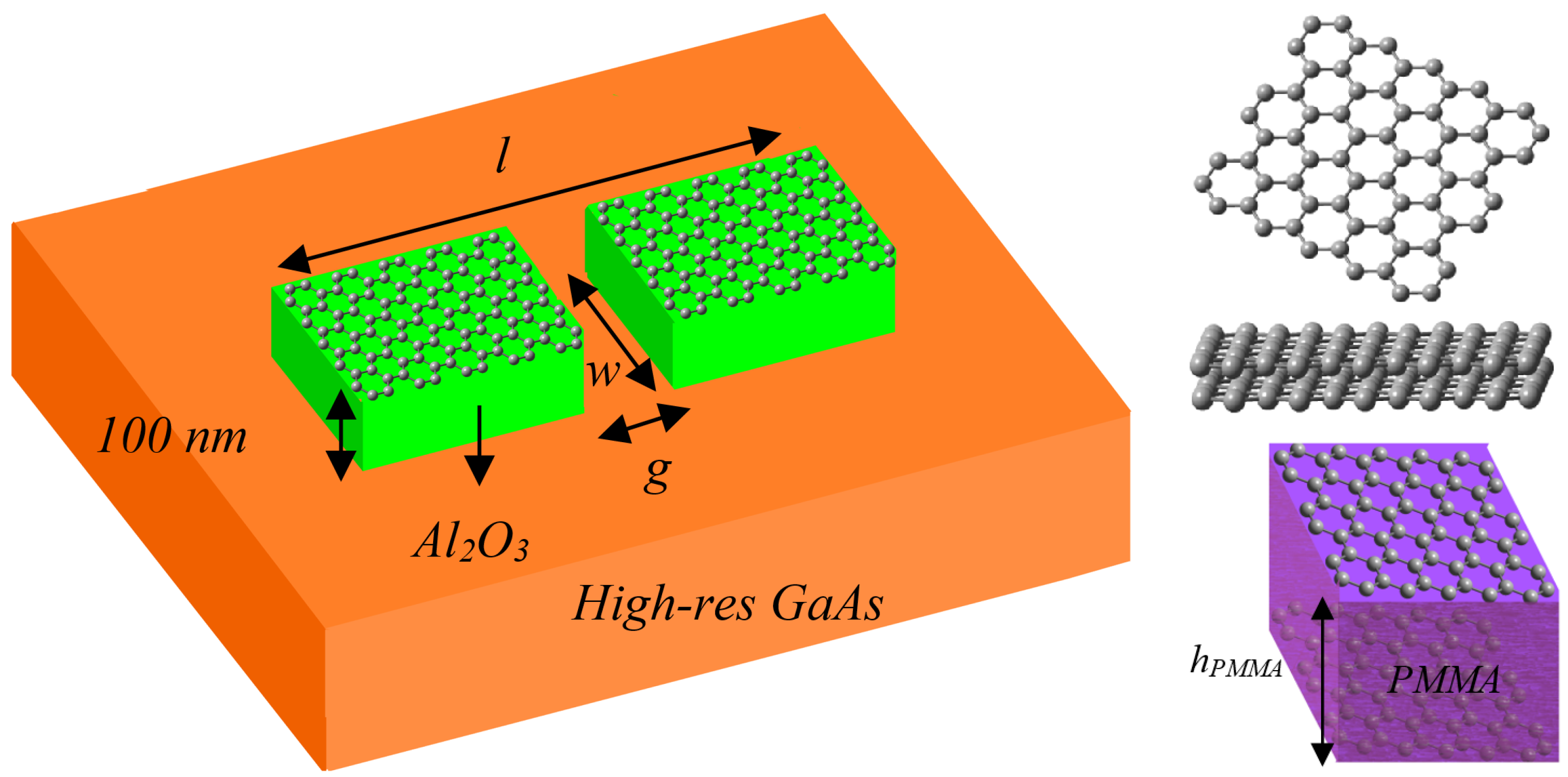
The antenna under study is basically a dipole of total length
l and width
w, as depicted in
Figure 1. Dipole arms are composed of a graphene structure, which can be either monolayer graphene, few-layer graphene, or a graphene stack, deposited on top of a thin dielectric layer –Aluminum Oxide (Al
2O
3) in our case. In the graphene stack case, a polymethylmethacrylate (PMMA) layer is used to act as a dielectric between the two graphene sheets. The substrate is considered high resistivity Gallium Arsenide (GaAs). To bring the design closer to experimental realization, we assume the dipole to be fed at its center gap of length
g with a terahertz photomixer that acts as a photoconductive source [
3]. It is worth mentioning that all the antennas considered in this work are compatible with widespread and even commercially available growth, transfer, and patterning methods for graphene [
3,
12,
13].
The remainder of the paper is as follows. In
Section 2, the investigation of the plasmonic modes supported by the different graphene waveguides is performed. This serves as a starting point for the design of graphene antenna structures, which are detailed and analyzed in
Section 3. The paper is concluded in
Section 4.
2. One-Dimensional and Two-Dimensional Plasmonic Waveguides Based on Graphene
In order to design and analyze an efficient plasmonic antenna, the investigation of the surface plasmon mode supported by its guided-wave structure is a primary step. Simplification of two-dimensional structures to one-dimensional structures is a reasonable starting point for their analysis. Therefore, consider three slab waveguides composed of monolayer graphene (MLG), few-layer graphene (FLG), and graphene stack (GS) as shown in
Figure 1. The resulting one-dimensional structures are thus GaAs-Al
2O
3-MLG-Air, GaAs-Al
2O
3-FLG-Air, and GaAs-Al
2O
3-GS-Air.
Although there is not a definitive consensus on the definition of FLG, most works consider it to be graphene sheets with no more than five layers [
9,
13,
14]. The optical conductivity of FLG is
[
13], where
is the surface conductivity of MLG calculated by the Kubo formula [
15] and
N is the number of layers. The reason for defining FLG for
is that this conductivity relation does not hold for more than five layers as interactions between adjacent layers cannot be ignored anymore and the conductivity approaches the values of bulk graphite [
13]. Throughout the paper, we consider two FLG instances: FLG2 for bi-layer graphene and FLG5 for the limit case of FLG with five layers. Intuitively, the higher conductivity of FLG should eventually lead to lower losses and, thus, higher efficiency.
In the case of GS, two graphene monolayers are separated by PMMA dielectric with height
. This value is chosen so that monolayers are far enough to disregard coupling through quantum effects [
16]. Dielectric constants
of GaAs, Al
2O
3, and PMMA are assumed 12.9, 9, and 2.4, respectively. The layer thickness of both Al
2O
3 and PMMA are assumed 100 nm, well within fabrication limits [
12], whereas the excitation frequency is 3 THz. Intuitively, antennas based on GS could provide higher efficiency through mode coupling and higher miniaturization due to their field confinement potential as sought in waveguide designs [
9].
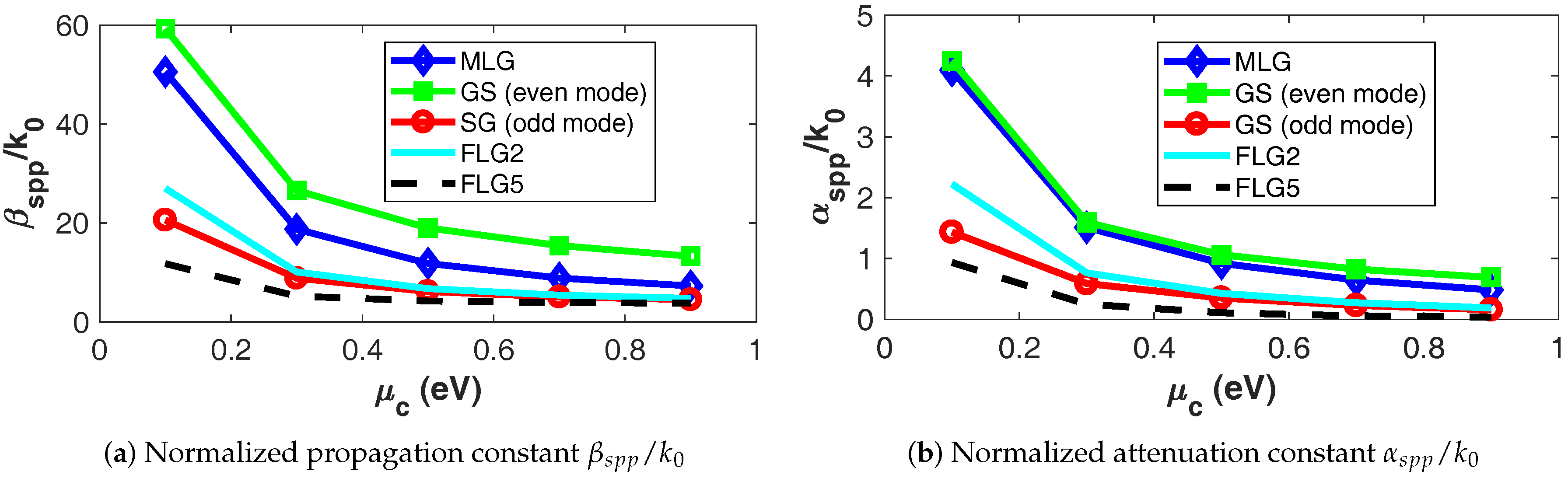
The transverse magnetic (TM) modes supported by the SPP waves for the waveguides are studied using the formulations of transfer matrix theory provided in our previous work [
17]. It is worth mentioning that there are two possible modes for GS structure, namely, the even mode, in which the normal electric fields is even symmetric; and the odd mode, in which the symmetry is odd.
Based on previous experiments and compatible with existing growth, encapsulation, and biasing techniques [
3,
12,
14], we assume the temperature, relaxation time, chemical potential of graphene to be 300 K, 0.6 ps, and 0.1–0.9 eV, respectively. With these figures, the normalized propagation constant
and normalized attenuation constant
of the evaluated structures are shown in
Figure 2.
These results regarding the behavior of plasmonic guided-wave structures can be employed to reason about the performance of graphene antennas as follows. In order to compare the miniaturization potential of the different antennas, the
–
chart shown in
Figure 2a is a suitable measure because the resonant length is inversely proportional to the effective index of the propagated mode. We thus observe that the even mode of GS structure has the highest confinement for the
values here considered, i.e.,
59.3–13.3, as expected; whereas the structure based on FLG with five layers has the lowest compactness among all structures, but with a suitable confinement factor nonetheless, i.e.,
11.8–3.8. FLG2 lies between MLG and FLG5.
On the other hand, a suitable qualitative measure of superiority of the structures from the perspective of radiation efficiency is the
–
chart shown in
Figure 2b. The reason is that the radiation efficiency has an inverse relation with the losses of the propagated mode. It is thus observed that the antenna based on FLG with five layers potentially provides the best radiation efficiency among the compared structures, as expected. Again, FLG2 shows a compromise between the efficiency of FLG5 and the miniaturization of MLG.
Let us now return to the two-dimensional guided-wave structure. We used the finite element method of the COMSOL field solver to perform the numerical calculations, including normal electric fields and effective refractive indices
of the structures as shown in
Figure 3. It is observed that the results of two-dimensional structures are similar to those of one-dimensional structures: FLG5 shows the lowest Im
denoting lowest losses, whereas GS has the highest Re
denoting highest confinement. The dependence with the width of the strip becomes clear: narrower strips are characterized by larger effective refractive index due to the higher confinement of moving charges. As discussed subsequently, this affects the antenna performance.
3. THz Plasmonic Antenna Based on MLG, FLG and GS
The antennas made of three kinds of guided-wave structures (MLG, FLG, and GS) are investigated as three-dimensional structures by the full-wave solver of the software CST Studio Suite.
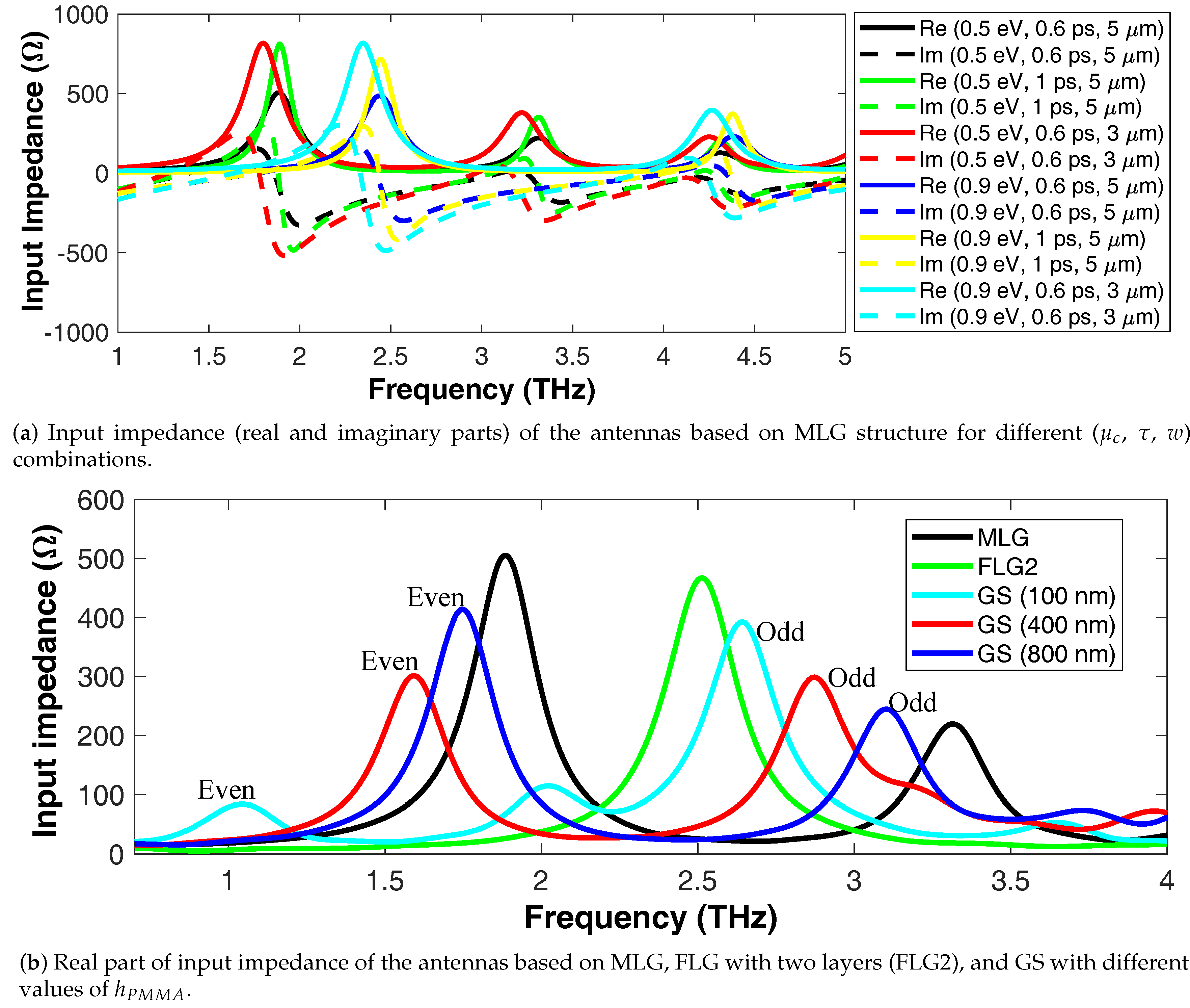
Assuming structural parameters of
l = 12 μm and
w = 3–5 μm, the real and imaginary parts of the input impedance of a MLG-based antenna are as shown in
Figure 4a. Different values for the parameters
and
, related to the graphene sheets, are considered. It is observed that the first resonance of the antenna, i.e., the imaginary part of the impedance is zero, has a low input impedance and it may be thus seen as a short-circuit resonance. The second resonance where the real and imaginary parts of input impedance are large can be interpreted as an open-circuit resonance. Contrary to in microwave antennas, the open-circuit resonance may be desired because it reduces the return loss when connecting the plasmonic antenna to THz sources that generally have high impedance. Considering
l = 12 μm,
w = 3 μm, g = 2 μm, τ = 0.6 ps, and
0.5 eV, the open-circuit resonance (
,
when
) occurs at 1.8 THz, which is lower than the
frequency predicted by the transmission line model because the dipole gap has non-negligible capacitance in this geometry.
In order to study the antennas based on FLG structure and compare them with antenna based on MLG structure, we present radiation efficiency
, miniaturization factor
, and input impedance
in
Table 1 for two values of chemical potential (0.5 and 0.9 eV), relaxation time (0.6 and 1 ps), and strip width (3 and 5
m). For the sake of brevity, we only present results for FLG with five layers. The results contained therein can be explained using the conclusions drawn from the guided-wave structures in
Section 2 as follows.
In both structures, changing chemical potentials from 0.5 to 0.9 eV causes the to decrease, therefore leading to a higher resonant frequency. Consequently, is greater because the antenna becomes electrically larger at resonance, while miniaturization factor is reduced. On the other hand, this change causes to decrease; resulting in the higher radiation efficiency because of a reduction of the ohmic loss of the antenna. In addition, implementing graphene with higher , which introduces lower loss, and also increasing w, which provides a larger electrically antenna, both result in a higher radiation efficiency.
Higher confinement by the use of a narrower strip or lower Fermi level increases the value of the input impedance. Moreover, higher (lower losses) causes a sharper resonance, resulting in larger input impedance in the open-circuit case.
Results also confirm that the FLG5 has higher radiation efficiency and lower miniaturization than MLG-based antennas. This is because the guided-wave structure based on FLG5 provides a mode propagating with a lower loss and a lower confinement compared to MLG structure. Since the conductivity of FLG5 starts to be comparable to that of bulk graphite, we do not expect that adding more layers would result in significant improvements. In any case, efficiency would increase slightly and miniaturization would drop.
Let us now compare the antenna based on FLG (only FLG2 with two layers for the sake of brevity), GS with different
values, and MLG with
12
m,
5
m,
0.5 eV, and
0.6 ps to further study miniaturization. Input impedance of the antennas is illustrated in
Figure 4b. The results can be explained by the effective indices of plasmonic modes as follows. The refractive indices of the structures based on MLG is 14.04, on FLG2 is 8.44, whereas on GS (odd and even modes) are 8.08 and 29.44 for
100 nm, 7.31 and 18.43 for
400 nm, and 6.43 and 16.15 for
800 nm at 3 THz. In light of these results, the most miniaturized antenna can be achieved with the even mode of GS structure. It should be mentioned that the results of GS antennas with large and small amounts of
is similar to MLG-based and FLG-based antennas, respectively. Generally, the results show that there is a tradeoff between miniaturization and radiation efficiency and the antenna based on FLG presents a suitable compromise, which can be further modulated by chosing the number of layers.

 ,
, 


