Pulsed Laser Fabrication of TiO2 Buffer Layers for Dye Sensitized Solar Cells


 , ,
, ,  and
and
Abstract
:
1. Introduction
2. Materials and Methods
2.1. Solar Cell Fabrication
2.2. Measurements
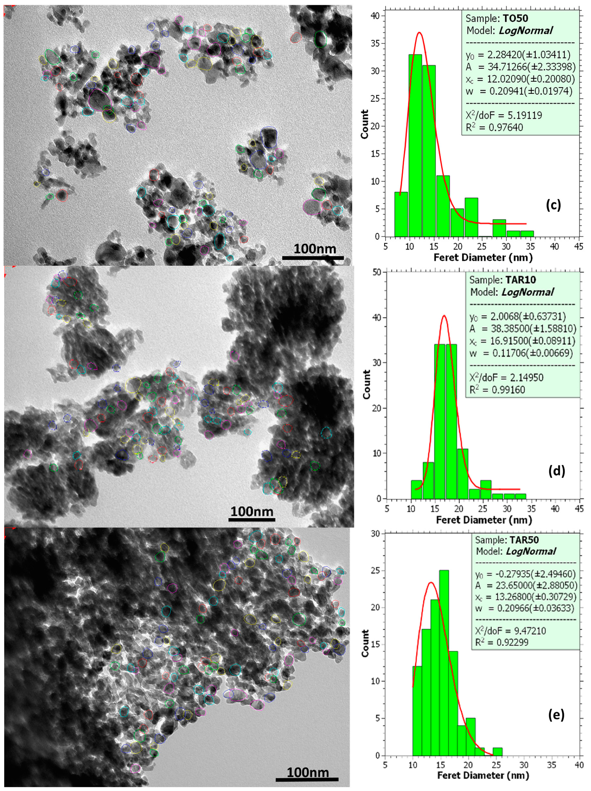
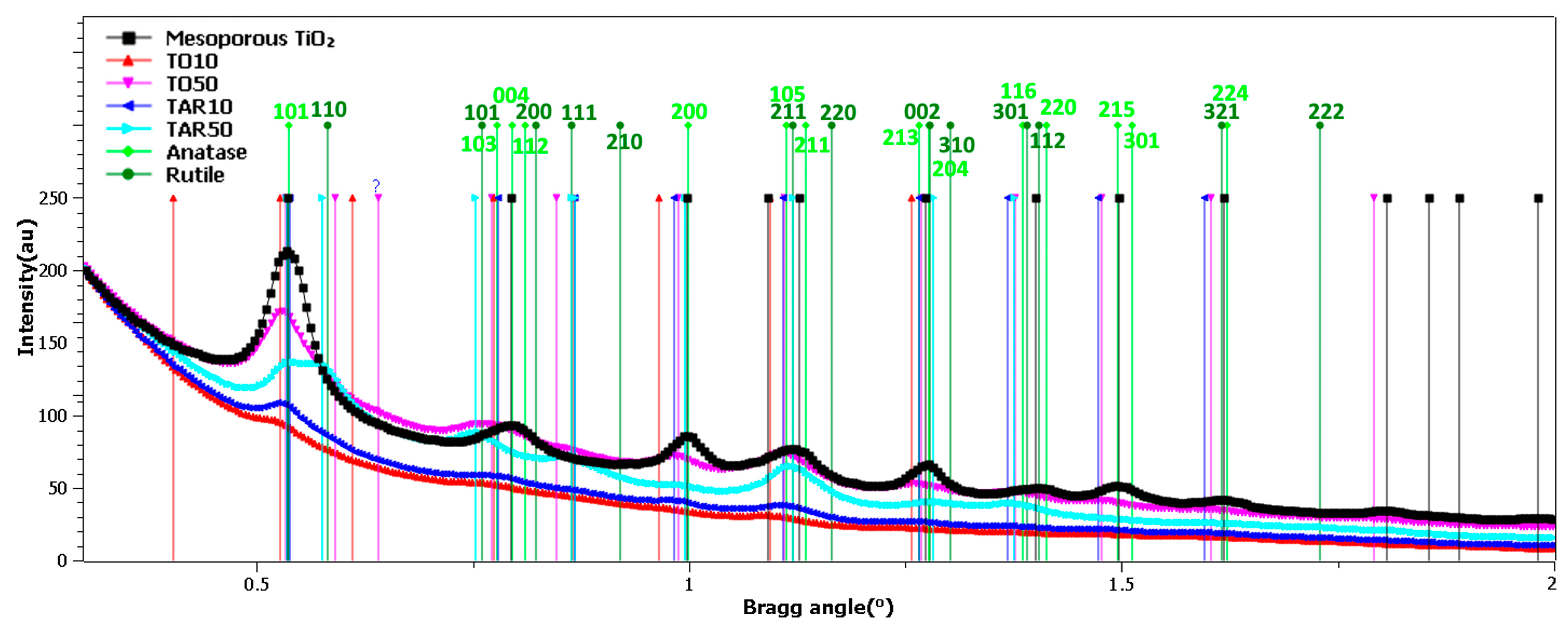
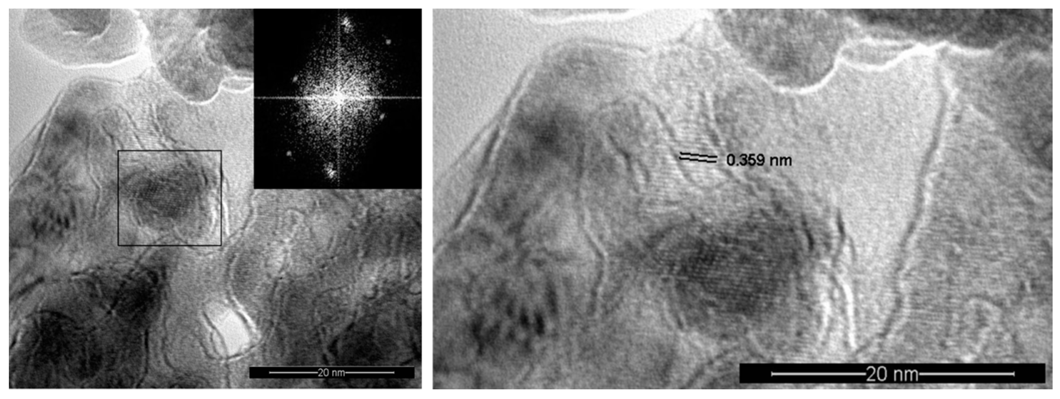
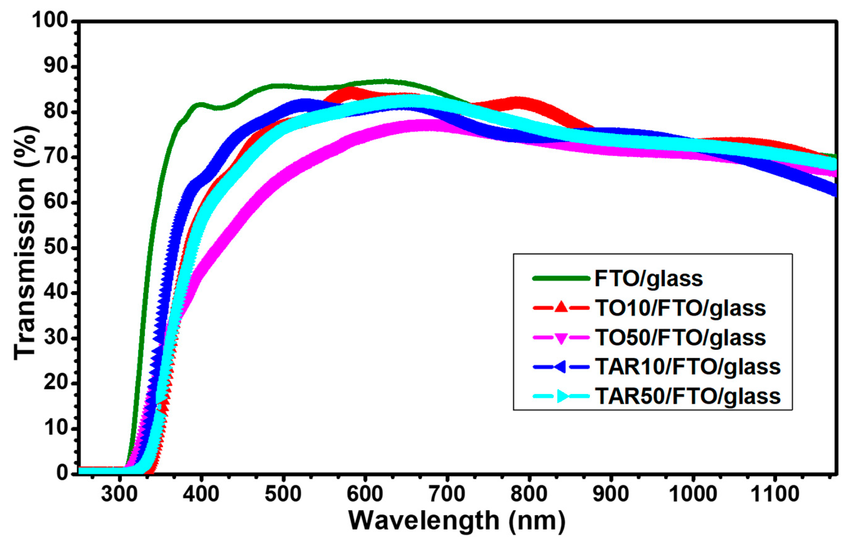
3. Results
4. Discussion
5. Conclusions
Supplementary Materials
Author Contributions
Funding
Acknowledgments
Conflicts of Interest
References
- Gong, J.; Sumathy, K.; Qiao, Q.; Zhou, Z. Review on dye-sensitized solar cells (DSSCs): Advanced techniques and research trends. Ren. Sust. En. Rev. 2017, 68, 234–246. [Google Scholar] [CrossRef]
- Freitag, M.; Teuscher, J.; Saygili, Y.; Zhang, X.; Giordano, F.; Liska, P.; Hua, J.; Zakeeruddin, S.M.; Moser, J.-E.; Grätzel, M.; Hagfeldt, A. Dye-sensitized solar cells for efficient power generation under ambient lighting. Nat. Photonics 2017, 11, 372–379. [Google Scholar] [CrossRef]
- O’Regan, B.; Grätzel, M. A low-cost, high-efficiency solar cell based on dye-sensitized colloidal TiO2 films. Nature 1991, 353, 737–740. [Google Scholar] [CrossRef]
- Gratzel, M. Photoelectrochemical Cells. Nature 2001, 414, 338–344. [Google Scholar] [CrossRef] [PubMed]
- Hagfeldt, A.; Boschloo, G.; Sun, L.; Kloo, L.; Pettersson, H. Dye-Sensitized Solar Cells. Chem. Rev. 2010, 110, 6595–6663. [Google Scholar] [CrossRef] [PubMed]
- Nazeeruddin, M.K.; Pechy, P.; Renouard, T.; Zakeeruddin, S.M.; Humphry-Baker, R.; Comte, P.; Liska, P.; Cevey, L.; Costa, E.; Shklover, V.; et al. Engineering of efficient panchromatic sensitizers for nanocrystalline TiO(2)-based solar cells. J. Am. Chem. Soc. 2001, 123, 1613–1624. [Google Scholar] [CrossRef]
- Nazeeruddin, M.K.; De Angelis, F.; Fantacci, S.; Selloni, A.; Viscardi, G.; Liska, P.; Ito, S.; Bessho, T.; Grätzel, M. Combined Experimental and DFT-TDDFT Computational Study of Photoelectrochemical Cell Ruthenium Sensitizers. J. Am. Chem. Soc. 2005, 127, 16835–16847. [Google Scholar] [CrossRef]
- Gratzel, M. Solar Energy Conversion by Dye-Sensitized Photovoltaic Cells. Inorg. Chem. 2005, 44, 6841–6851. [Google Scholar] [CrossRef]
- Robertson, N. Catching the rainbow: Light harvesting in dye-sensitized solar cells. Angew. Chem. Int. Ed. 2008, 47, 1012–1014. [Google Scholar] [CrossRef]
- Xie, Y.; Tang, Y.; Wu, W.; Wang, Y.; Liu, J.; Li, X.; Tian, H.; Zhu, W.-H. Porphyrin Cosensitization for a Photovoltaic Efficiency of 11.5%: A Record for Non-Ruthenium Solar Cells Based on Iodine Electrolyte. J. Am. Chem. Soc. 2015, 137, 14055–14058. [Google Scholar] [CrossRef]
- Yella, A.; Lee, H.W.; Tsao, H.N.; Yi, C.; Chandiran, A.K.; Nazeeruddin, M.K.; Diau, E.W.G.; Yeh, C.Y.; Zakeeruddin, S.M.; Gratzel, M. Porphyrin-Sensitized Solar Cells with Cobalt (II/III)—Based Redox Electrolyte Exceed 12 Percent Efficiency. Science 2011, 334, 629–634. [Google Scholar] [CrossRef] [PubMed]
- Kenji Kakiage, K.; Aoyama, Y.; Yano, T.; Oya, K.; Kyomen, T.; Hanaya, M. Fabrication of a high-performance dye-sensitized solar cell with 12.8% conversion efficiency using organic silyl-anchor dyes. Chem. Commun. 2015, 51, 6315–6317. [Google Scholar] [CrossRef] [PubMed]
- Liu, M.; Johnston, M.B.; Snaith, H.J. Efficient planar heterojunction perovskite solar cells by vapour deposition. Nature 2013, 501, 395–398. [Google Scholar] [CrossRef]
- Yang, W.S.; Park, B.-W.; Jung, E.H.; Jeon, N.J.; Kim, Y.C.; Lee, D.U.; Shin, S.S.; Seo, J.; Kim, E.K.; Noh, J.H.; et al. Iodide management informamidinium-lead-halide–basedperovskite layers for efficientsolar cells. Science 2017, 356, 1376–1379. [Google Scholar] [CrossRef]
- Yu, H.; Zhang, S.Q.; Zhao, H.J.; Will, G.; Liu, P.B. An Efficient and Low-Cost TiO2 Compact Layer for Performance Improvement of Dye-Sensitized Solar Cells. Electrochim. Acta 2009, 54, 1319–1324. [Google Scholar] [CrossRef]
- Patrocinio, A.O.T.; Paterno, L.G.; Iha, N.Y.M. Layer-by-layer TiO2 films as efficient blocking layers in dye-sensitized solar cells. J. Photochem. Photobiol. A 2009, 205, 23–27. [Google Scholar] [CrossRef]
- Ito, S.; Murakami, T.N.; Comte, P.; Liska, P.; Gratzel, C.; Nazeeruddin, M.K.; Grätzel, M. Fabrication of Thin Film Dye Sensitized Solar Cells with Solar to Electric Power Conversion Efficiency over 10%. Thin Solid Films 2008, 516, 4613–4619. [Google Scholar] [CrossRef]
- Wang, P.; Zakeeruddin, S.M.; Comte, P.; Charvet, R.; Humphry-Baker, R.; Grätzel, M. Enhance the Performance of Dye-Sensitized Solar Cells by Co-grafting Amphiphilic Sensitizer and Hexadecylmalonic Acid on TiO2 Nanocrystals. J. Phys. Chem. B 2003, 107, 4336–143341. [Google Scholar] [CrossRef]
- Kim, J.H.; Lee, K.J.; Roh, J.H.; Song, S.W.; Park, J.H.; Yer, I.H.; Moon, B.M. Ga-doped ZnO transparent electrodes with TiO2 blocking layer/nanoparticles for dye-sensitized solar cells. Nano. Res. Lett. 2012, 7, 1–12. [Google Scholar] [CrossRef]
- Yoo, B.; Kim, K.J.; Bang, S.Y.; Ko, M.J.; Kim, K.; Park, N.G. Chemically deposited blocking layers on FTO substrates: Effect of precursor concentration onphotovoltaic performance of dye-sensitized solar cells. J. Electroanal. Chem. 2010, 638, 161–166. [Google Scholar] [CrossRef]
- Lungu, J.; Ştefan, N.; Prodan, G.; Georgescu, A.; Mandeș, A.; Ciupina, V.; Mihăilescu, I.N.; Gîrțu, M.A. Characterization of spin-coated TiO2 buffer layers for dye-sensitized solar cells. Digest J. Nanomat. Biostruct. 2015, 10, 967–976. [Google Scholar]
- Kavan, L.; O’Regan, B.; Kay, A.; Grätzel, M. Preparation of TiO2 (anatase) films on electrodes by anodic oxidative hydrolysis of TiCl3. J. Electroanal. Chem. 1993, 346, 291–307. [Google Scholar] [CrossRef]
- Kavan, L.; Tetreault, N.; Moehl, T.; Grätzel, M. Electrochemical Characterization of TiO2 Blocking Layers for Dye-Sensitized Solar Cells. J. Phys. Chem. C 2014, 118, 16408–16418. [Google Scholar] [CrossRef]
- Kavan, L.; Grätzel, M. Highly efficient semiconductingTiO2 photoelectrodes prepared by aerosol pyrolysis. Electrochim. Acta 1995, 40, 643–652. [Google Scholar] [CrossRef]
- Cameron, P.J.; Peter, L.M. Characterization of Titanium Dioxide Blocking Layers in Dye-Sensitized Nanocrystalline Solar Cells. J. Phys. Chem. B 2003, 107, 14394–14400. [Google Scholar] [CrossRef]
- Peng, B.; Jungmanna, G.; Jäger, C.; Haarer, D.; Schmidt, H.-W.; Thelakkat, M. Systematic investigation of the role of compact TiO2 layer in solid state dye-sensitized TiO2 solar cells. Coord. Chem. Rev. 2004, 248, 1479–1489. [Google Scholar] [CrossRef]
- Ito, S.; Zakeeruddin, S.; Humphry-Baker, R.; Liska, P.; Charvet, R.; Comte, P.; Nazeeruddin, M.; Péchy, P.; Takata, M.; Miura, H.; et al. High-Efficiency Organic-Dye-Sensitized Solar Cells Controlled by Nanocrystalline-TiO2 Electrode Thickness. Adv. Mater. 2006, 18, 1202. [Google Scholar] [CrossRef]
- Burke, A.; Ito, S.; Snaith, H.; Bach, U.; Kwiatkowski, J.; Grätzel, M. The Function of a TiO2 Compact Layer in Dye-Sensitized Solar Cells Incorporating “Planar” Organic Dyes. Nano Lett. 2008, 8, 977–981. [Google Scholar] [CrossRef] [PubMed]
- Hart, J.N.; Menzies, D.; Cheng, Y.B.; Simon, G.P.; Spiccia, L. TiO2 sol-gel blocking layers for dye-sensitized solar cells. C. R. Chimie 2006, 9, 622–626. [Google Scholar] [CrossRef]
- Kavan, L.; Zukalova, M.; Vik, O.; Havlicek, D. Sol–Gel Titanium Dioxide Blocking Layers for Dye- Sensitized Solar Cells: Electrochemical Characterization. ChemPhysChem 2014, 15, 1056–1061. [Google Scholar] [CrossRef]
- Ito, S.; Liska, P.; Comte, P.; Charvet, R.; Pechy, P.; Bach, U.; Schmidt-Mende, L.; Zakeeruddin, S.M.; Kay, A.; Nazeeruddin, M.K.; et al. Control of dark current in photoelectrochemical (TiO2/I−–I3−) and dye-sensitized solar cells. Chem. Commun. 2005, 4351–4353. [Google Scholar] [CrossRef]
- Xia, J.; Masaki, N.; Jiang, K.; Yanagida, S. Deposition of a Thin Film of TiOx from a Titanium Metal Target as Novel Blocking Layers at Conducting Glass/TiO2 Interfaces in Ionic Liquid Mesoscopic TiO2 Dye-Sensitized Solar Cells. J. Phys. Chem. B 2006, 110, 25222–25228. [Google Scholar] [CrossRef]
- Hitosugi, T.; Yamada, N.; Nakao, S.; Hirose, Y.; Hasegawa, T. Properties of TiO2-based transparent conducting oxides. Phys. Status Solidi A 2010, 207, 1529–1537. [Google Scholar] [CrossRef]
- Braga, A.; Baratto, C.; Colombi, P.; Bontempi, E.; Salvinelli, G.; Drera, G.; Sangaletti, L. An ultrathin TiO2 blocking layer on Cd stannate as highly efficient front contact for dye-sensitized solar cells. Phys. Chem. Chem. Phys. 2013, 15, 16812–16818. [Google Scholar] [CrossRef] [PubMed]
- Thelakkat, M.; Schmitz, C.; Schmidt, H.-W. Fully vapor-deposited thin-layer titanium dioxide solar cells. Adv. Mater. 2002, 14, 577–581. [Google Scholar] [CrossRef]
- Hamann, T.W.; Martinson, A.B.F.; Elam, J.W.; Pellin, M.J.; Hupp, J.T. Atomic Layer Deposition of TiO2 on Aerogel Templates: New Photoanodes for Dye-Sensitized Solar Cells. J. Phys. Chem. C 2008, 112, 10303–10307. [Google Scholar] [CrossRef]
- Van Delft, J.A.; Garcia-Alonso, D.; Kessels, W.M.M. Atomic layer deposition for photovoltaics: Applications and prospects for solar cell manufacturing. Semicond. Sci. Technol. 2012, 27, 074002. [Google Scholar] [CrossRef]
- Chandiran, A.K.; Yella, A.; Stefik, M.; Heiniger, L.P.; Comte, P.; Nazeeruddin, M.K.; Grätzel, M. Low-Temperature Crystalline Titanium Dioxide by Atomic Layer Deposition for Dye-Sensitized Solar Cells. ACS Appl. Mater. Interfaces 2013, 5, 3487–3493. [Google Scholar] [CrossRef] [PubMed]
- Gan, W.Y.; Lam, S.W.; Chiang, K.; Amal, R.; Zhao, H.; Brungs, M.P. Novel TiO2 thin film with non-UV activated superwetting and antifogging behaviours. J. Mater. Chem. 2007, 17, 952–954. [Google Scholar] [CrossRef]
- Charbonneau, C.; Cameron, P.J.; Pockett, A.; Lewis, A.; Troughton, J.R.; Jewell, E.; Worsley, D.A.; Watson, T.M. Solution processing of TiO2 compact layers for 3rd generation photovoltaics. Ceram. Int. 2016, 42, 11989–11997. [Google Scholar] [CrossRef]
- Bai, Y.; Xing, Z.; Yu, H.; Li, Z.; Amal, R.; Wang, L. Porous Titania Nanosheet/Nanoparticle Hybrids as Photoanodes for Dye-Sensitized Solar Cells. ACS Appl. Mater. Interfaces 2013, 5, 12058–12065. [Google Scholar] [CrossRef] [Green Version]
- Lee, S.; Noh, J.H.; Han, H.S.; Yim, D.Y.; Kim, D.H.; Lee, J.-K.; Kim, J.Y.; Jung, H.S.; Hong, K.S. Nb-Doped TiO2: A New Compact Layer Material for TiO2 Dye-Sensitized Solar Cells. J. Phys. Chem. C 2009, 113, 6878–6882. [Google Scholar] [CrossRef]
- Zhou, W.-Q.; Lu, Y.-M.; Chen, C.-Z.; Liu, Z.-Y.; Cai, C.-B. Effect of Li-doped TiO2 Compact Layers for Dye Sensitized Solar Cells. J. Inorg. Mater. 2011, 26, 819–822. [Google Scholar] [CrossRef]
- Bäuerle, D. Laser Processing and Chemistry; Springer: Berlin, Germany, 1996. [Google Scholar]
- Gyorgy, E.; Socol, G.; Axente, E.; Mihailescu, I.N.; Ducu, C.; Ciuca, S. Anatase phase TiO2 thin films obtained by pulsed laser deposition for gas sensing applications. Appl. Surf. Sci. 2005, 247, 429–433. [Google Scholar] [CrossRef]
- Mihailescu, I.N.; Gyorgy, E. Pulsed laser deposition: An overview. In Proceedings of the Invited Contribution to the Fourth International Commission for Optics (ICO) Book Trends in Optics and Photonics; Asakura, T., Ed.; Springer: Berlin, Germany, 1999; 201p. [Google Scholar]
- Pechini, M. Method of preparing lead and alkaline earth titanates and niobates and coating method using the same to form a capacitor. US Patent 3 330 697, 1967. [Google Scholar]
- Hocevar, M.; Opara, U.; Krasovec, U.; Berginc, M.; Drazic, G.; Hauptman, N.; Topic, M. Development of TiO2 pastes modified with Pechini sol–gel method for high efficiency dye-sensitized solar cell. J. Sol. Gel Sci. Technol. 2008, 48, 156–162. [Google Scholar] [CrossRef]
- Opara, U.; Krasovec, U.; Berginc, M.; Hocevar, M.; Topic, M. Unique TiO2 paste for high efficiency dye-sensitized solar cells. Sol. Energy Mater. Sol. Cells 2009, 93, 379–381. [Google Scholar] [CrossRef]
- Nezeeruddin, M.K.; Kay, A.; Rodicio, I.; Humphry-Baker, R.; Muller, E.; Liska, P.; Vlachopoulos, N.; Grätzel, M. Conversion of Light to Electricity by cis-XzBis(2,2′-bipyridyl-4,4′-dicarboxylate)ruthenium(11) Charge-Transfer Sensitizers (X = C1-, Br-, I-, CN-, and SCN-) on Nanocrystalline TiO2 Electrodes. J. Am. Chem. Soc. 1993, 115, 6382–6390. [Google Scholar] [CrossRef]
- Millington, K.R.; Fincher, K.W.; King, A.L. Mordant dyes as sensitisers in dye-sensitised solar cells. Sol. Energy Mater. Sol. Cells 2007, 91, 1618–1630. [Google Scholar] [CrossRef]
- Smestad, G.P.; Grätzel, M. Demonstrating Electron Transfer and Nanotechnology: A Natural Dye–Sensitized Nanocrystalline Energy Converter. J. Chem. Educ. 1998, 75, 752–756. [Google Scholar] [CrossRef]
- Teodorescu, V.S.; Blanchin, M.G. Fast and Simple Specimen Preparation for TEM Studies of Oxide Films Deposited on Silicon Wafers. Microsc. Microanal. 2009, 15, 15–19. [Google Scholar] [CrossRef]
- Dimitriu, E.; Iuga, A.; Ciupina, V.; Prodan, G.; Ramer, R. PZT-type materials with improved radial piezoelectric properties. J. Eur. Ceram. Soc. 2005, 25, 2401–2404. [Google Scholar] [CrossRef]
- Georgescu, A.; Damache, G.; Gîrţu, M.A. Class A small area solar simulator for dye-sensitized solar cell testing. J. Optoelectron. Adv. Mater. 2008, 10, 3003–3007. [Google Scholar]
- Mihailescu, I.N.; Gyorgy, E.; Teodorescu, V.S.; Steinbrecker, G.; Neamtu, J.; Perrone, A.; Luches, A. Characteristic features of the laser radiation-target interactions during reactive pulsed laser ablation of Si targets in ammonia. J.Appl. Phys. 1999, 86, 7123–7128. [Google Scholar] [CrossRef]
- Mihailescu, I.N.; Teodorescu, V.S.; Gyorgy, E.; Luches, A.; Perrone, A.; Martino, M. About the nature of particulates covering the surface of thin films obtained by reactive pulsed laser deposition. J. Phys. D Appl. Phys. 1998, 31, 2236–2240. [Google Scholar] [CrossRef]
- Mihailescu, I.N.; Teodorescu, V.S.; Gyorgy, E.; Ristoscu, C.; Cristescu, R. Particulates in pulsed laser deposition: Formation mechanisms and possible approaches to their elimination. In Proceedings of the SPIE International Conference of ALT’01, Constanta, Romania, 11–14 September 2001; Volume 4762, pp. 64–74. [Google Scholar]
- Hovmöller, S. CRISP: Crystallographic image processing on a personal computer. Ultramicroscopy 1992, 41, 121–135. [Google Scholar]
- Zou, X.D.; Sukharev, Y.; Hovmöller, S. ELD — a computer program system for extracting intensities from electron diffraction patterns. Ultramicroscopy 1993, 49, 147–158. [Google Scholar] [CrossRef]
- Wyckoff, R.W.G. Crystal Structures; Interscience Publishers: New York, NY, USA, 1963; Volume 1, pp. 253–254. [Google Scholar]
- Meagher, E.P.; George, A.L. Polyhedral thermal expansion in the TiO2 polymorphs: Refinement of the crystal structures of rutile and brookite at high temperature. Can. Miner. 1979, 17, 77–85. [Google Scholar]
- Halme, J.; Vahermaa, P.; Miettunen, K.; Lund, P. Device physics of dye solar cells. Adv. Mater. 2010, 22, 210–234. [Google Scholar] [CrossRef]
- Hamann, T.W.; Jensen, R.A.; Martinson, A.B.F.; van Ryswykac, H.; Hupp, J.T. Advancing beyond current generation dye-sensitized solar cells. Energy Environ. Sci. 2008, 1, 66–78. [Google Scholar] [CrossRef]
- Chrisey, D.G.; Hubler, G.K. Pulsed Laser Deposition of Thin Films; Wiley: New York, NY, USA, 1994. [Google Scholar]
- Von Allmen, M.; Blatter, A. Laser–Beam Interactions with Materials, 2nd ed.; Springer: Berlin, Germany, 1995. [Google Scholar]


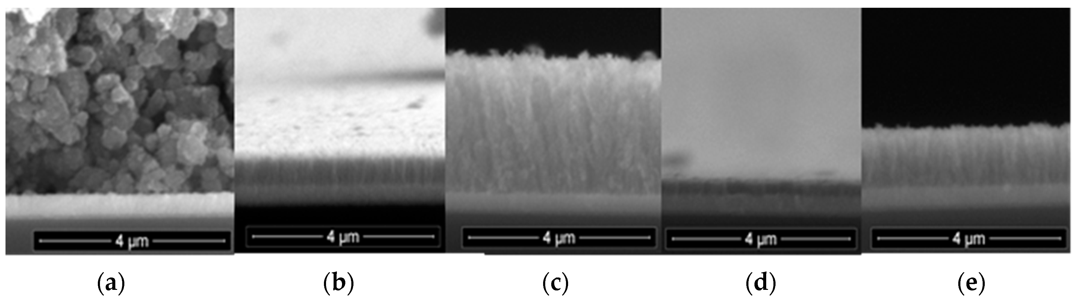
| Film Type | TiO2 Mesoporous Film | TO10 Buffer Layer | TO50 Buffer Layer | TAR10 Buffer Layer | TAR50 Buffer Layer |
|---|---|---|---|---|---|
| Thickness (µm) | ~29.89 | ~0.65 | ~2.95 | ~0.33 | ~1.24 |
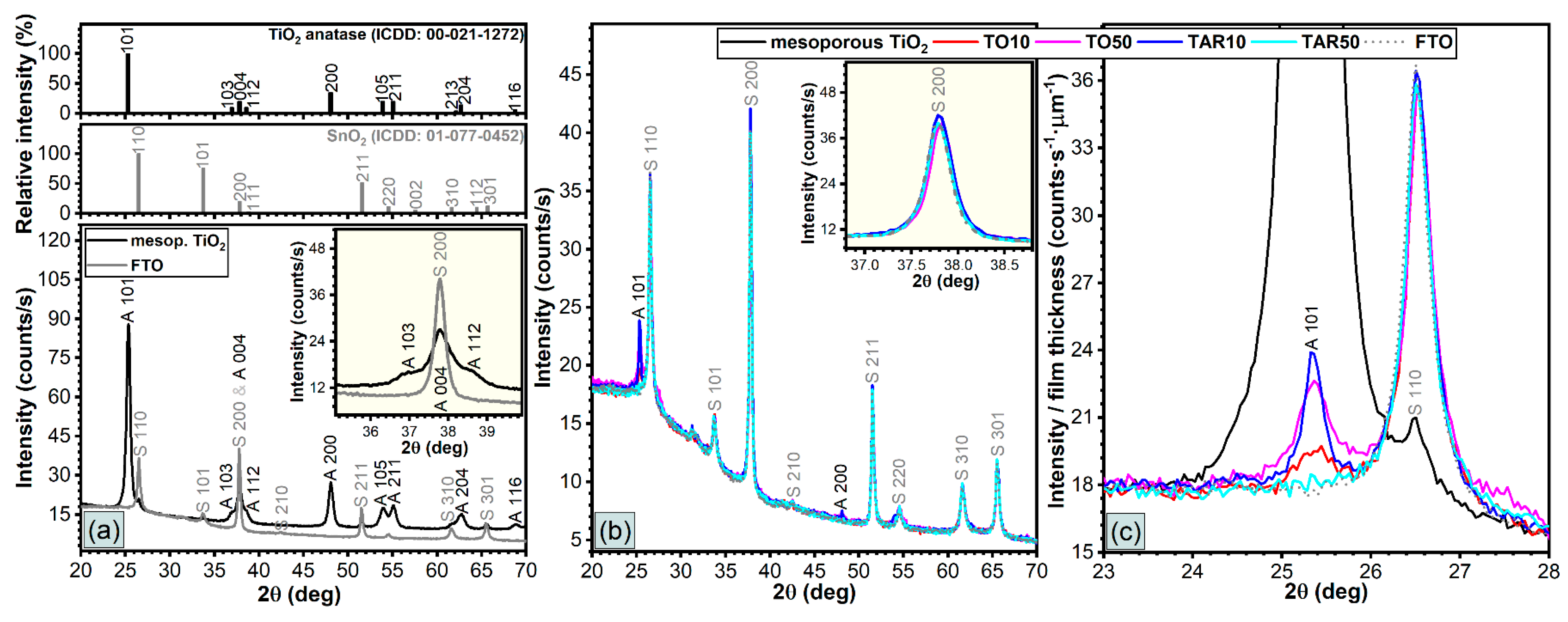
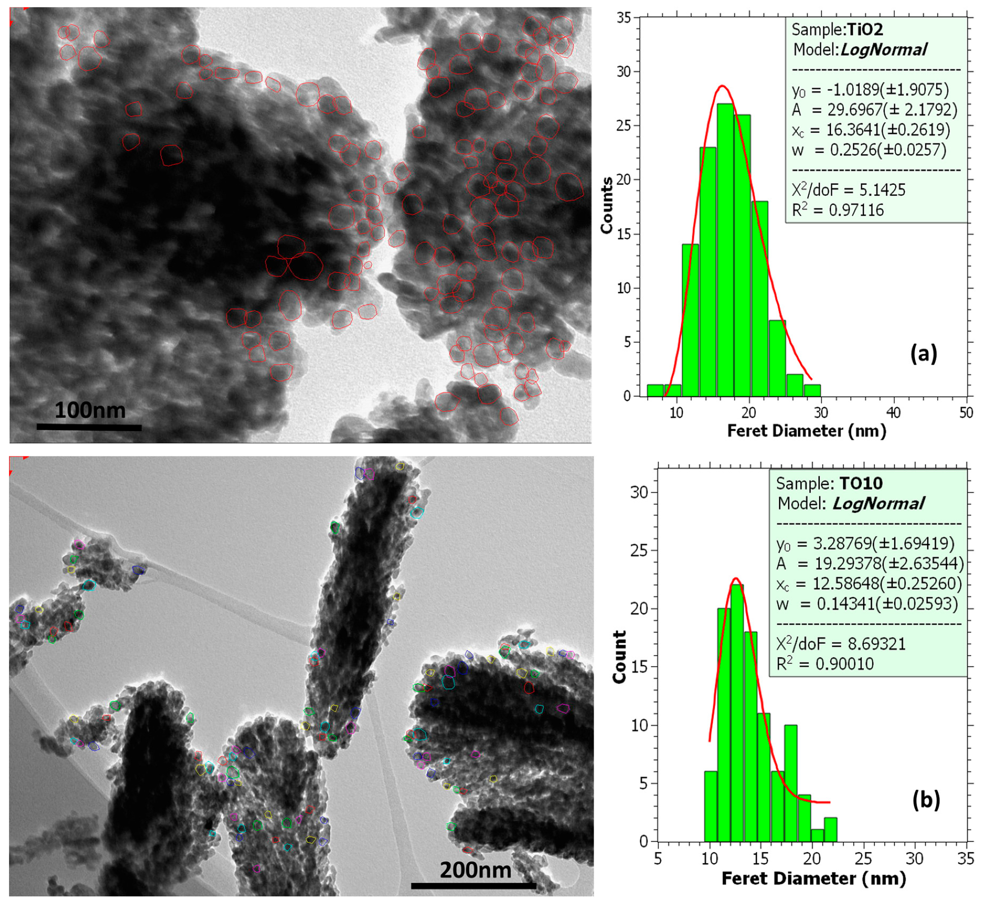
| TiO2 Layer Type | XRD (101) Crystalline Coherent Length (nm) | TEM Mean Grain Size (nm) |
|---|---|---|
| TO10 | ~21.5 | 12.6 |
| TO50 | ~28.1 | 12.0 |
| TAR10 | ~40.8 | 16.9 |
| TAR50 | n/a | 13.3 |
| Mesoporous film | ~19.0 | 16.4 |
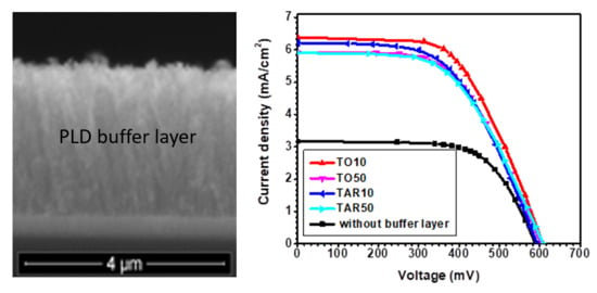
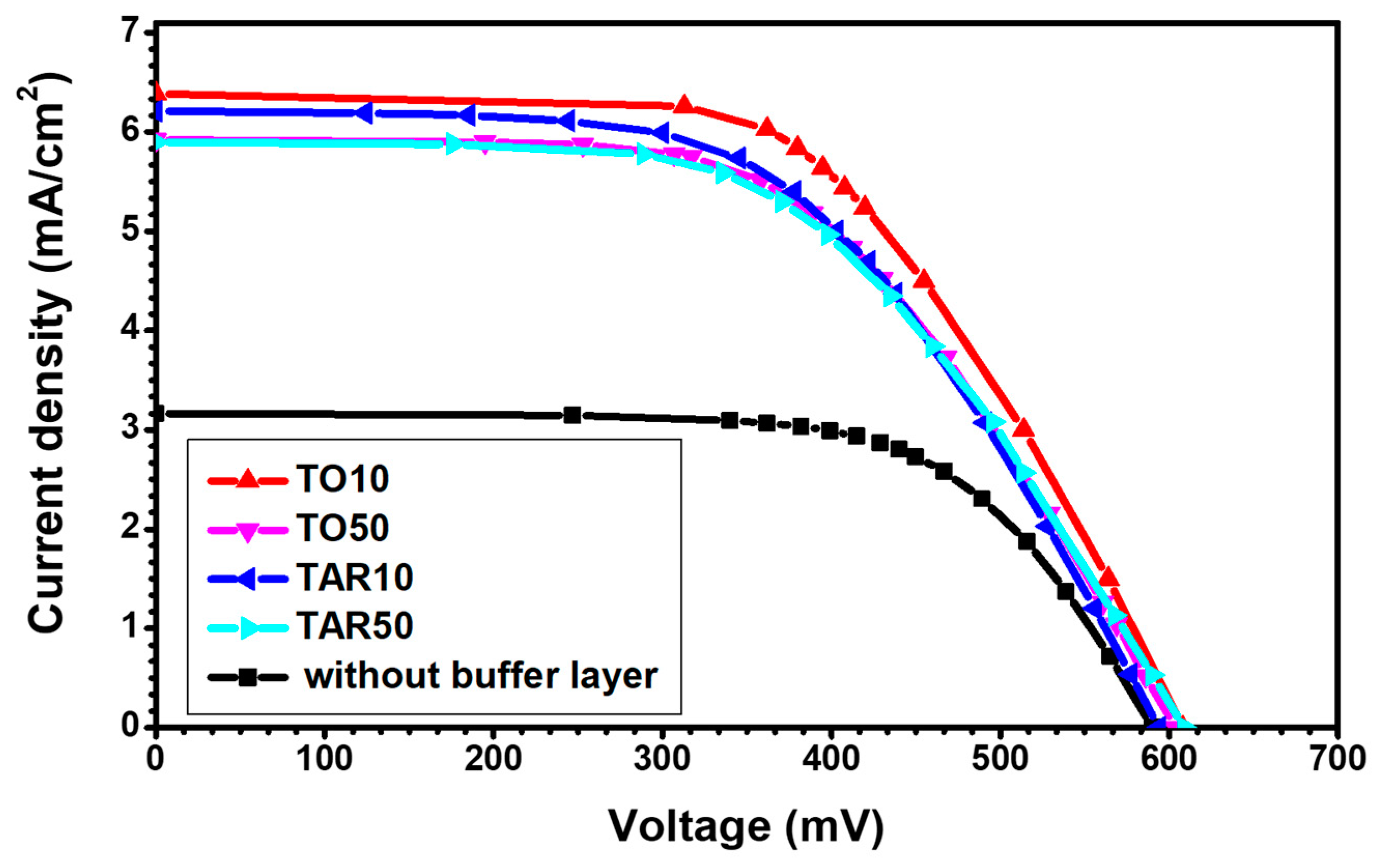
| Sample | Isc (mA) | Voc (mV) | Jsc (mA/cm2) | Pmax (μW) | FF | η (%) |
|---|---|---|---|---|---|---|
| TO10 | 6.39 | 608 | 8.136 | 2228 | 0.57 | 2.84 |
| TO50 | 5.92 | 604 | 7.537 | 2015 | 0.56 | 2.57 |
| TAR10 | 6.21 | 594 | 7.907 | 2041 | 0.55 | 2.60 |
| TAR50 | 5.90 | 609 | 7.512 | 1978 | 0.55 | 2.52 |
| No buffer | 2.48 | 590 | 3.166 | 968 | 0.66 | 1.23 |
© 2019 by the authors. Licensee MDPI, Basel, Switzerland. This article is an open access article distributed under the terms and conditions of the Creative Commons Attribution (CC BY) license (http://creativecommons.org/licenses/by/4.0/).
Share and Cite
Lungu, J.; Socol, G.; Stan, G.E.; Ştefan, N.; Luculescu, C.; Georgescu, A.; Popescu-Pelin, G.; Prodan, G.; Gîrţu, M.A.; Mihăilescu, I.N. Pulsed Laser Fabrication of TiO2 Buffer Layers for Dye Sensitized Solar Cells. Nanomaterials 2019, 9, 746. https://doi.org/10.3390/nano9050746
Lungu J, Socol G, Stan GE, Ştefan N, Luculescu C, Georgescu A, Popescu-Pelin G, Prodan G, Gîrţu MA, Mihăilescu IN. Pulsed Laser Fabrication of TiO2 Buffer Layers for Dye Sensitized Solar Cells. Nanomaterials. 2019; 9(5):746. https://doi.org/10.3390/nano9050746
Chicago/Turabian StyleLungu, Jeanina, Gabriel Socol, George E. Stan, Nicolaie Ştefan, Cătălin Luculescu, Adrian Georgescu, Gianina Popescu-Pelin, Gabriel Prodan, Mihai A. Gîrţu, and Ion N. Mihăilescu. 2019. "Pulsed Laser Fabrication of TiO2 Buffer Layers for Dye Sensitized Solar Cells" Nanomaterials 9, no. 5: 746. https://doi.org/10.3390/nano9050746