Beam Tailoring Devices Using Transmission-Type Subwavelength Grating


School of Science, Lanzhou University of Technology, Lanzhou 730050, China
*
Author to whom correspondence should be addressed.
Photonics 2023, 10(6), 607; https://doi.org/10.3390/photonics10060607
Submission received: 31 March 2023
/
Revised: 3 May 2023
/
Accepted: 18 May 2023
/
Published: 23 May 2023
Abstract
:Subwavelength gratings (SWGs) possess an excellent ability to manipulate the wavefronts of light waves. We investigated the beam tailoring mechanism of aperiodic SWGs in our current work, and a bifocal lens, a beam splitter, and a beam combiner based on transmission-type one-dimensional SWGs are presented and simulated here. By designing grating nanobar parameters to meet the predetermined phase shift profile of the diffraction light, desired beam steering is accurately achieved for the three devices while maintaining high transmissivity. All the simulated results show good agreement with the theoretical predictions.
1. Introduction
In the past decades, all-dielectric metamaterials, commonly known as synthetic subwavelength-engineered material, have always been the focus of intense research in the field of optical devices, which can be designed to manipulate the properties of transmitted light [1]. Meanwhile, two-dimensional photonic crystal waveguides (WGs) have opened a new direction for designing photonic crystal sensors [2], all-optical full-adders [3], resonators [4], and so on. However, their obscurity regarding production and their inherent diffraction losses restrict the range of applications [5]. Moreover, most previous studies on metamaterials have lacked rigorous theoretical calculations and derivations. Subwavelength gratings (SWGs), in part, can be considered as subwavelength-scale photonic crystals and are emerging as an enabling technology for implementing compact, high-performance photonic integrated devices and circuits [6,7], including reflectors [8], directional couplers [9], filters [10], splitters [11], sensors [12], and modulators [13], among others. Moreover, certain subwavelength gratings with novel surface structures can greatly improve device performance [14].
Recently, with the development and demonstration of array optical devices and spatial imaging technology, the crosswise controlling of the wavefront in a reflected or transmitted mode has made significant progress [15,16], as one-dimensional and two-dimensional SWGs exhibit interesting behavior in the field of integrated optoelectronic devices due to their excellent abilities of spatial beam controlling [17,18]. With the help of localized phase front tailoring, the phase, amplitude, and polarization of reflected or transmitted waves at the interface between two mediums could be manipulated in the near-infrared communication band. There are applications in optoelectronic devices using SWGs, e.g., beam deflection, beam focusing, and beam splitting. Usually, SWGs are used to integrate with optically active devices to improve their performance and enhance their coupling efficiency, and thus, they can hardly be made into a single membrane. However, the silicon-on-insulator (SOI) platform is extremely attractive for realizing high-capacity SWGs, which makes it possible for us to test the performance of the SWGs-based devices [19]. Moreover, the SOI platform is fully compatible with mature CMOS technology and is widely used as a substrate for making various silicon-photonics devices [20].
In this paper, we summarize our recent work on developing beam tailoring devices, and a bifocal lens, a beam splitter, and a beam combiner based on non-periodic one-dimensional SWGs are proposed and demonstrated. For a bifocal lens, the incident beam is concentrated on two different focal planes along the optical axes, which is similar to the eyes of certain insects in the extant animal kingdom [21]. Theoretically, SWGs can play the part of multifocal lenses, which have several applications in the field of beam manipulation and spatial imaging. As an example, a bifocal lens with two focal planes at 10 μm and 20 μm, respectively, behind the surface of the grating is demonstrated and simulated using the finite element method (FEM). For a beam splitter, an incident beam could be split into multiple beams in different directions and the split beams can be parallel or converge at different focal points. As an example, a beam splitter with a power ratio of 1:2 and two deflection angles of 15° and 30°, respectively, is demonstrated and simulated. Moreover, a beam combiner based on SWG is proposed, which could combine multiple non-coherent light beams into a single one, it provides an effective way of increasing the output power of the laser. The simulated results indicated that the SWGs-based bifocal lens, beam splitter, and beam combiner exhibit excellent beam-tailoring characteristics. The wavefront control ability of SWGs is verified through the design of these devices. Moreover, we hope to apply these novel devices to optoelectronic integration and spatial imaging.
2. Theoretical Background
For a periodic SWG, the diffraction efficiencies and phase shift of the incident wave can be calculated for both transverse electric (TE) and transverse magnetic (TM) polarization through the use of the rigorous coupled-wave analysis (RCWA) [22]. Its conclusions can be extended to non-periodic gratings by splicing multiple regions with different design wisdoms, and high refractive indexed grating nanobars can manipulate the localized phase of the diffraction beam [17]. The overall effect is that the desired phase distribution can be obtained while maintaining a high reflectivity/transmissivity. SWG with a beam-steering ability has been reported in [23], which is a typical application of one-dimensional SWG for spatial beam control.
For the three devices proposed in this paper, silicon nanobars are patterned on an SOI platform due to the design flexibility. The design of aperiodic SWGs relies on the calculations of transmittance and wavefront phase in periodic SWGs of different sizes, and the phase spectrum should span a complete 2π when nanobar width changes. To obtain higher transmittance, the optimal thickness of the top silicon layer is set to 0.8 µm at an operational wavelength of 1.55 µm under normal incidence. It should be noted that TE incident light can only achieve a complete 2π phase coverage and a higher transmittance simultaneously in one-dimensional SWGs with difficulty; therefore, the devices mentioned in this paper are all based on TM polarization transmission-type SWGs. The transmittance and phase spectra as functions of the period Λ and duty cycle η for TM incident waves are shown in Figure 1, where the periods of the nanobars range from 0.4 μm to 1.2 μm and the duty cycles range from 0.3 to 0.8. These two diagrams have provided a phase categorization table for obtaining the necessary phase shift in the design process of the gratings with special performances.
3. Design Process and Numerical Simulation
3.1. SWG Bifocal Lens
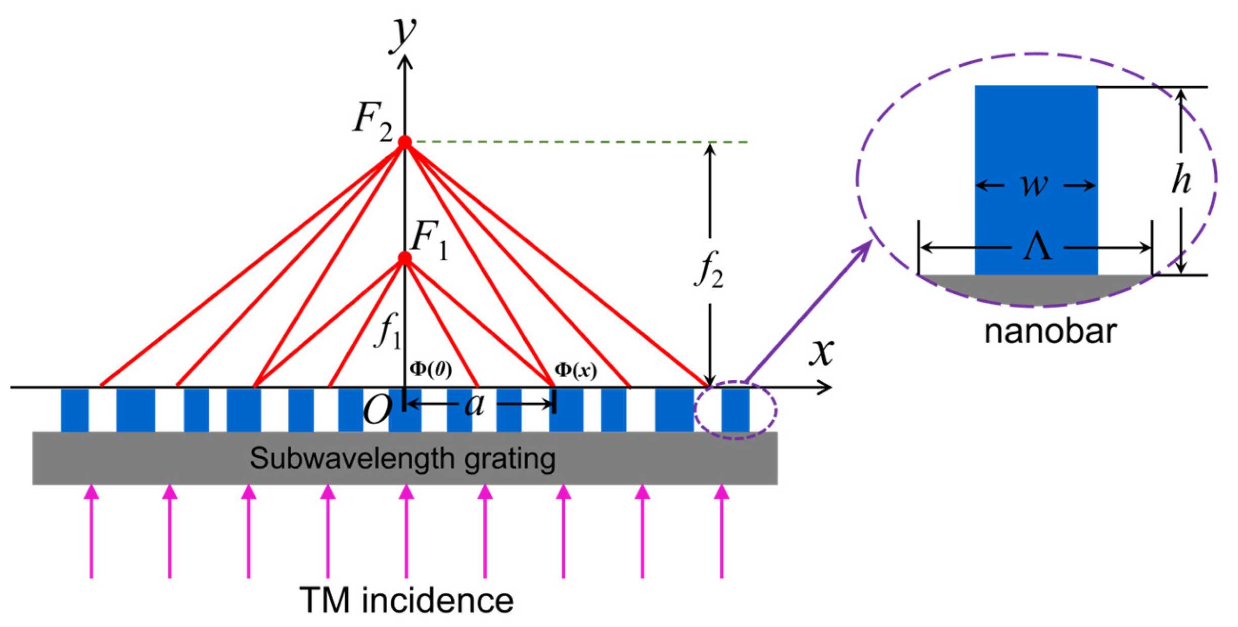
Bifocal lenses and multifocal lenses are important optical elements, which have always been an enticing topic in the field of bionics and spatial imaging [24,25]. An SWG-based bifocal lens can achieve similar functions. The schematic diagram of the proposed SWG bifocal lens is shown in Figure 2, and the width and period of the nanobar are denoted as w and Λ, respectively, while all the nanobars have the same height h; therefore, the duty cycle can be expressed as η = w/Λ. The vertically incident light will be split into two beams according to the desired power ratio; each beam will be concentrated on its focal plane along the optical axes, as shown by F1 and F2 in Figure 2; and the corresponding focal lengths are f1 and f2, respectively. In the coordinate system shown in Figure 2, the desired phase profile of the transmitted light wavefront is demonstrated below:
where Φ(x) is the local phase of the transmitted light wavefront on the transmission plane, Φ(0) is the local phase at the center of the grating (origin of coordinates), λ is the vacuum wavelength of the incident light, f1 is the first focal length, f2 is the second focal length, and the value of a determines the power ratio of two foci. According to the desired phase profile, silicon nanobars with maximum possible transmittance are selected one by one from center to periphery by searching the phase categorization table shown in Figure 1. As an example, we have designed an SWG bifocal lens with two focal planes are at 10 μm and 20 μm, respectively, behind the surface of the grating, where the total grating width is 50.8 μm, the grating height is 0.8 µm, and a is set to be 15 μm.
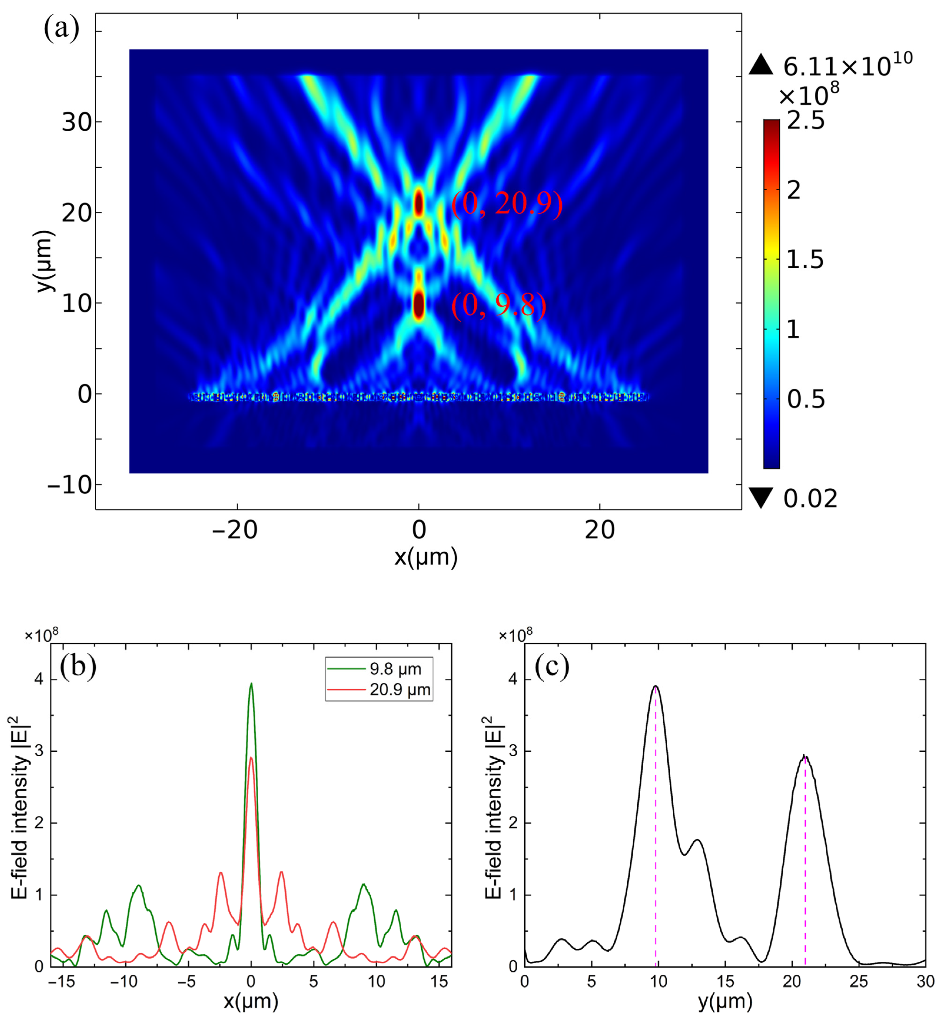
To verify the splitting and focusing ability of the SWG bifocal lens, the numerical simulation of the grating is performed using the FEM at an operational wavelength of 1.55 μm, the perfectly matched layer (PML) boundaries are considered in both the x and y-directions. TM normal incident waves illuminate upon the substrate of the wafer and then converge at two different foci behind the grating surface. Figure 3a shows the numerically simulated field distribution of the transmitted wave. It is apparent that the incident light converges at two spots, which are at around 9.8 μm and 20.9 μm behind the surface of the grating lens, respectively, and the total transmittance of the grating is around 89%. The simulated results show a good agreement with the design value. The factor, which may contribute to the error, is discontinued in the phase modulation and a limited number of SWG elements. Figure 3b shows the field distributions on these two focal planes and demonstrates that the peaks occur on the optical axes, and the full width at half maximums (FWHMs) of the electric field intensity at two foci are around 1.12 µm and 1.14 µm, respectively. In Figure 3c, the peaks along the optical axes are represented by pink dashed lines, which indicate the accurate position of two focal planes, the depth of foci can also be obtained. The conclusion drawn from the above simulation is that a bifocal lens can be easily obtained using SWGs. It should be noted that the results regarding the one-dimensional nanobar grating can be extended to the two-dimensional circular grating [26], thus realizing the true bifocal lens in the three-dimensional space. Related works are in progress.
3.2. SWG Beam Splitter
A beam splitter is an important optical element in integrated optical circuits. A number of novel technologies can realize beam splitting, such as metasurface [27], diffraction grating [28], plasmon waveguide [29], and others. In this section, we investigate the feasibility of developing SWG-based beam splitters. The schematic diagram of the proposed SWG bifocal splitter is shown in Figure 4. A normal incident beam will be split into two beams according to the predetermined power ratio and steering angles denoted as α and β in the figure. In the coordinate system shown in Figure 5, the desired phase profile of the transmitted light wavefront can be written as:
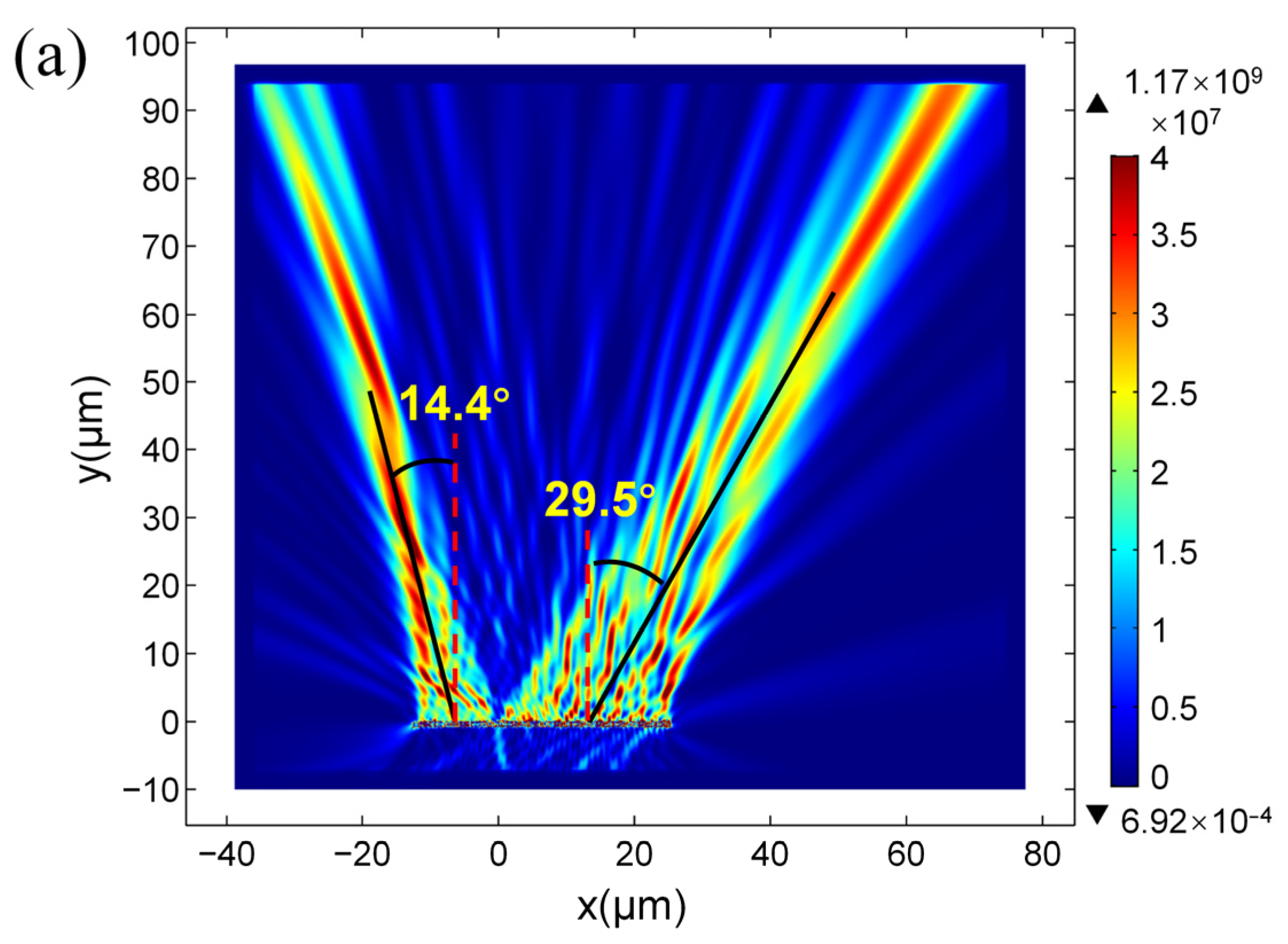
As an example, we designed an SWG beam splitter with two steering angles, α = 15° and β = 30°, while the splitting power ratio is 1:2, which is determined by the grating area. The numerical simulation of this grating is performed at an operational wavelength of 1.55 μm under TM normal incidence. Figure 5a shows the e-field propagating in the SWG beam splitter. The simulated deflection angles of the two transmitted beams are 14.4° and 29.5°, respectively, and the splitting power ratio is around 1:1.87, which are close to the theoretical values. The total transmittance of the grating is around 85%. E-field distributions on three cross-sections with different distances behind the grating surface are shown in Figure 5b, and it is clearly evident that the FWHMs of the electric field along the split beam are almost constant; in other words, the split beams are still parallel.
3.3. SWG Beam Combiner
The function of the beam combiner is the opposite of that of the beam splitter, which is commonly used to combine multiple lasers with lower power and achieve high brightness and high beam quality [30]. The schematic diagram of the proposed SWG beam combiner is shown in Figure 6, in which the two incoherent beams with different incidence angles are combined into one beam, and the desired phase profile of the transmitted light wavefront can be written as:
where ΔΦ(x) = Φ′(x) − Φ(x) is the phase change of the transmitted light wavefront at a random position x, while Φ(x) is the phase of the incident light on the incident plane and Φ′(x) is the phase of the transmitted light on the transmission plane at the corresponding position x. ΔΦ(0) = Φ′(0) − Φ(0) is the phase change of the transmitted light wavefront at a position x = 0, while Φ(0) is the phase of the incident light on the incident plane, and Φ′(0) is the phase of the transmitted light on the transmission plane at the corresponding position x = 0. Here, we use phase change because the beam is an oblique incidence and cannot use transmission phase to replace the phase change.
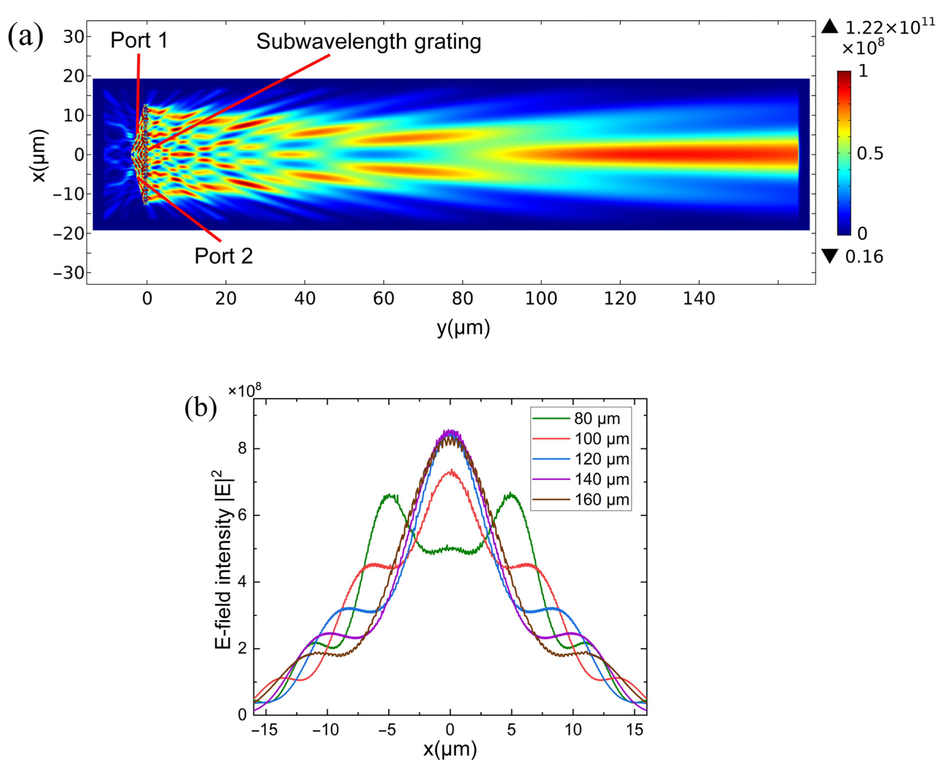
An SWG beam combiner with incidence angles α = β = 15° and a transmitted beam perpendicular to the transmission surface (theoretically, the transmission angle can be an arbitrary value of less than 90°) is proposed. The numerical simulation of the beam combiner is performed at a wavelength of 1.55 μm. Figure 7a shows the e-field propagating in the SWG beam combiner, and e-field distributions on several planes at different distances along the optical axes are plotted in Figure 7b. It is clearly evident that the FWHMs of the transmission spectrum remain largely the same at the distances of y = 120 μm, y = 140 μm, and y = 160 μm, which indicates that the transmitted light is a parallel beam. The total transmittance of the grating is around 91.3%. The simulated results show a good agreement with theoretical predictions.
4. Conclusions
In this article, a bifocal lens, a beam splitter, and a beam combiner, based on transmission-type one-dimensional SWGs, are proposed in order to demonstrate the excellent beam tailoring ability of SWGs fabricated on an SOI wafer. We choose the optimized thickness of the top silicon layer, when the periods of the nanobars range from 0.4 μm to 1.2 μm and the duty cycles range from 0.3 to 0.8, and the complete 2π phase modulation of the transmitted wave could be achieved while maintaining a high transmissivity, which provides a theoretical basis for device design. An SWG bifocal lens with two focal planes at 10 μm and 20 μm, respectively, behind the grating surface, is designed and simulated, the simulated results are around 9.8 μm and 20.9 μm, respectively, which indicate that the proposed bifocal lens was able to produce two distinct and well-focused images along the optical axes. An SWG beam splitter with two steering angles, α = 15° and β = 30°, is proposed, and the simulated results are around 14.4° and 29.5°, respectively. Moreover, an SWG beam combiner with the incidence angle α = β = 15° is presented, the simulated results indicate that the transmitted light is a parallel beam. All the simulated results show good agreement with theoretical values, through which the wavefront control ability of SWGs is demonstrated.
5. Discussion
The proposed bifocal lens, beam splitter, and beam combiner in this paper are all based on one-dimensional nanobar subwavelength gratings; however, the conclusions of the one-dimensional nanobar SWGs can be extended to two-dimensional circular SWGs and two-dimensional block SWGs. It should be noted that two-dimensional block SWGs have better spatial beam controlling abilities [31], and related research is ongoing. Moreover, these SWGs-based beam tailoring devices on SOI platforms are easy to fabricate with standard photolithography, and perfectly prepared strip subwavelength gratings using electron beam lithography and inductive coupled plasma etching techniques have been reported in many relevant studies [32]. The fabrication of two-dimensional block gratings was also mentioned in our previous work [31]. We envision the near-future application of SWGs-based devices in the field of beam reshaping, spatial imaging, and integrated optics.
Author Contributions
Methodology, G.W.; Software, Z.Y.; Investigation, J.L.; Resources, S.H.; Data curation, G.W.; writing—original draft preparation, G.W.; review and editing, all authors. All authors have read and agreed to the published version of the manuscript.
Funding
This research was funded by the National Nature Science Foundation of China (NSFC), grant number 61665005.
Institutional Review Board Statement
Not applicable.
Informed Consent Statement
Not applicable.
Data Availability Statement
The data presented in this study are available on request from the corresponding author.
Conflicts of Interest
The authors declare no conflict of interest.
References
- Choi, M.; Leem, J.W.; Yu, J.S. Optical performance improvement of semitransparent metal film electrodes with biomimetic SWGs for high-performance optoelectronic device applications. RSC Adv. 2015, 5, 84865–84871. [Google Scholar] [CrossRef]
- Parandin, F.; Heidari, F.; Rahimi, Z.; Olyaee, S. Two-dimensional photonic crystal biosensors: A review. Opt. Laser Technol. 2021, 144, 107397. [Google Scholar] [CrossRef]
- Maleki, M.J.; Mir, A.; Soroosh, M. Design and analysis of a new compact all-optical full-adder based on photonic crystals. Optik 2021, 227, 166107. [Google Scholar] [CrossRef]
- Benmerkhi, A.; Bounouioua, A.; Bouchemat, M. Two-dimensional photonic crystal resonator for high pressure sensing. In Proceedings of the Applied Nanotechnology and Nanoscience International Conference, Paris, France, 24 March 2021. [Google Scholar]
- Vlasov, Y.A.; Moll, N.; McNab, S.J. Intrinsic diffraction losses in 2D SOI photonic crystal waveguides. In Proceedings of the International Quantum Electronics Conference, San Francisco, CA, USA, 21 May 2004; pp. 823–824. [Google Scholar]
- Wang, J.; Glesk, I.; Chen, L.R. Subwavelength grating devices in silicon photonics. Sci. Bull. 2016, 61, 879–888. [Google Scholar] [CrossRef]
- Chang-Hasnain, C.J. High-contrast gratings as a new platform for integrated optoelectronics. Semicond. Sci. Technol. 2011, 26, 014043. [Google Scholar] [CrossRef]
- Zohar, M.; Auslender, M.; Hava, S. Ultrathin high efficiency photodetectors based on SWG and near-field enhanced absorption. Nanoscale 2015, 7, 5476–5479. [Google Scholar] [CrossRef]
- Xie, H.; Zheng, J.J.; Xu, P.P.; Yao, J.T.; Whitehead, J.; Majumdar, A. Ultra-compact subwavelength-grating-assisted polarization-independent directional coupler. IEEE Photonics Technol. Lett. 2019, 31, 1538–1541. [Google Scholar] [CrossRef]
- Sumi, R.; Gupta, N.D.; Das, B.K. Integrated optical linear edge filters using apodized sub-wavelength grating waveguides in SOI. IEEE Photonics Technol. Lett. 2019, 31, 1449–1452. [Google Scholar] [CrossRef]
- Ma, M.; Park, A.H.K.; Wang, Y.; Shoman, H.; Zhang, F.; Jaeger, N.; Chrostowski, L. Sub-wavelength grating-assisted polarization splitter-rotators for silicon-on-insulator platforms. Opt. Express 2019, 27, 17581–17591. [Google Scholar] [CrossRef]
- Tahmasebpour, M.; Bahrami, M.; Asgari, A. Design of a high figure of merit subwavelength grating based plasmonic sensor for detection of DNA hybridization. Optik 2015, 126, 2747–2751. [Google Scholar] [CrossRef]
- Cencillo-Abad, P.; Plum, E.; Rogers, E.T.; Zheludev, N. Spatial optical phase-modulating metadevice with subwavelength pixelation. Opt. Express 2016, 24, 18790–18798. [Google Scholar] [CrossRef]
- Chen, J.; Zhang, M.X.; Gu, P.; Weng, Z.Y.; Yan, Z.D.; Gao, F.; Tang, C.J.; Yan, B.; Zhu, M.W. Silver mirror for enhancing the magnetic plasmon resonance and sensing performance in plasmonic metasurface. Appl. Phys. Express 2022, 15, 102003. [Google Scholar] [CrossRef]
- Yuan, Y.; Sun, M.Y.; Bi, Y.; Gao, W.N.; Zhang, S.; Zhang, W.P. Controlling the light wavefront through a scattering medium based on direct digital frequency synthesis technology. Chin. Phys. B 2021, 30, 014209. [Google Scholar] [CrossRef]
- Liang, X.B.; Li, Y.Q.; Liu, K. Wide dynamic range wavefront sensor using sub-wavelength grating array. Opt. Commun. 2015, 347, 68–74. [Google Scholar] [CrossRef]
- Fattal, D.; Li, J.; Peng, Z.; Fiorentino, M.; Beausoleil, R.G. Flat silicon grating reflectors with high focusing power. Opt. Photonics News 2010, 21, 42. [Google Scholar] [CrossRef]
- Arbabi, A.; Horie, Y.; Ball, A.J.; Bagheri, M.; Faraon, A. Subwavelength-thick lenses with high numerical apertures and large efficiency based on high contrast transmitarrays. Nat. Commun. 2015, 6, 7069. [Google Scholar] [CrossRef]
- Kaur, H.; Kumar, M. Two-way reflector based on two-dimensional sub-wavelength high-index contrast grating on SOI. Opt. Commun. 2016, 366, 266–270. [Google Scholar] [CrossRef]
- Halir, R.; Cheben, P.; Schmid, J.H.; Ma, R.; Bedard, D.; Janz, S.; Xu, D.X.; Densmore, A.; Lapointe, J.; Molina-Fernandez, I. Continuously apodized fiber-to-chip surface grating coupler with refractive index engineered subwavelength structure. Opt. Lett. 2010, 35, 3243–3245. [Google Scholar] [CrossRef]
- Stowasser, A.; Rapaport, A.; Layne, J.E.; Morgan, R.C.; Buschbeck, E.K. Biological Bifocal Lenses with Image Separation. Curr. Biol. 2010, 20, 1482–1486. [Google Scholar] [CrossRef]
- Moharam, M.G.; Grann, E.B.; Pommet, D.A.; Gaylord, T.K. Formulation for stable and efficient implementation of the rigorous coupled-wave analysis of binary gratings. J. Opt. Soc. Am. A 1995, 12, 1068–1076. [Google Scholar] [CrossRef]
- Ma, C.L.; Huang, Y.Q.; Duan, X.F.; Ren, X.M. High-transmissivity non-periodic sub-wavelength high-contrast grating with large-angle beam-steering ability. Chin. Opt. Lett. 2014, 12, 120501. [Google Scholar] [CrossRef]
- Gal, J.; Horvath, G.; Clarkson, E.N.K.; Haiman, O. Image formation by bifocal lenses in a trilobite eye? Vision Res. 2000, 40, 843–853. [Google Scholar] [CrossRef] [PubMed]
- Kroger, R.H.H.; Campbell, M.C.W.; Fernald, R.D.; Wagner, H.J. Multifocal lenses compensate for chromatic defocus in vertebrate eyes. J. Comp. Physiol. A 1999, 184, 361–369. [Google Scholar] [CrossRef]
- Ma, C.L.; Huang, Y.Q.; Ren, X.M. High-numerical-aperture high-reflectivity focusing reflectors using concentric circular high-contrast gratings. Appl. Opt. 2015, 54, 973–978. [Google Scholar] [CrossRef] [PubMed]
- Zhang, P.; Zhang, C.C.; Yang, Y.Y.; Ke, L.; Fang, B.; Li, C.X.; Hong, Z.; Jing, X.F. Polarization sensitive terahertz all dielectric continuous trapezoid metasurface beam splitter. Infrared Phys. Technol. 2023, 130, 104604. [Google Scholar] [CrossRef]
- Torcal-Milla, F.J.; Sanchez-Brea, L.M. Design and numerical analysis of metallic Ronchi diffraction gratings acting as reflective beam-splitter. Optik 2022, 271, 170119. [Google Scholar] [CrossRef]
- Yang, J.B.; Xin, H.; Han, Y.X.; Chen, D.B.; Zhang, J.J.; Huang, J.; Zhang, Z.J. Ultra-compact beam splitter and filter based on a graphene plasmon waveguide. Appl. Opt. 2017, 56, 9814–9821. [Google Scholar] [CrossRef]
- Wang, J.; Zhang, Y.; Lv, P.; Sun, Q. Simulation method of non-ideal light source in laser system. Infrared Laser Eng. 2014, 11, 3527–3530. (In Chinese) [Google Scholar]
- Wu, G.; Huang, Y.Q.; Duan, X.F.; Liu, K.; Niu, H.J.; Ren, X.M. Light control elements as convex cylindrical lens and concave cylindrical mirror based on 2D high-index contrast gratings. Jpn. J. Appl. Phys. 2020, 59, 062003. [Google Scholar] [CrossRef]
- Takashima, Y.; Haraguchi, M.; Naoi, Y. High-sensitivity refractive index sensor with normal incident geometry using a subwavelength grating operating near the ultraviolet wavelength. Sens. Actuators B 2018, 255, 1711–1715. [Google Scholar] [CrossRef]
Figure 1.
(a) Transmittance spectrum and (b) phase spectrum of periodic 1D subwavelength gratings.

Figure 2.
Schematic of SWG bifocal lens on an SOI wafer.

Figure 3.
(a) Field distribution of the SWG bifocal lens, (b) field distribution on the focal plane, and (c) e-field intensity along the optical axes.
Figure 3.
(a) Field distribution of the SWG bifocal lens, (b) field distribution on the focal plane, and (c) e-field intensity along the optical axes.

Figure 4.
The schematic of an SWG beam splitter on an SOI wafer.

Figure 5.
(a) E-field distribution of the SWG beam splitter and (b) field distribution on sections with different distances behind the grating surface.
Figure 5.
(a) E-field distribution of the SWG beam splitter and (b) field distribution on sections with different distances behind the grating surface.


Figure 6.
Schematic of SWG beam combiner on an SOI wafer.

Figure 7.
(a) E-field distribution of the SWG beam combiner and (b) field distribution on sections with different distances behind the grating surface.
Figure 7.
(a) E-field distribution of the SWG beam combiner and (b) field distribution on sections with different distances behind the grating surface.

Disclaimer/Publisher’s Note: The statements, opinions and data contained in all publications are solely those of the individual author(s) and contributor(s) and not of MDPI and/or the editor(s). MDPI and/or the editor(s) disclaim responsibility for any injury to people or property resulting from any ideas, methods, instructions or products referred to in the content. |
© 2023 by the authors. Licensee MDPI, Basel, Switzerland. This article is an open access article distributed under the terms and conditions of the Creative Commons Attribution (CC BY) license (https://creativecommons.org/licenses/by/4.0/).
Share and Cite
MDPI and ACS Style
Wu, G.; Hou, S.; Lei, J.; Yan, Z. Beam Tailoring Devices Using Transmission-Type Subwavelength Grating. Photonics 2023, 10, 607. https://doi.org/10.3390/photonics10060607
AMA Style
Wu G, Hou S, Lei J, Yan Z. Beam Tailoring Devices Using Transmission-Type Subwavelength Grating. Photonics. 2023; 10(6):607. https://doi.org/10.3390/photonics10060607
Chicago/Turabian StyleWu, Gang, Shanglin Hou, Jingli Lei, and Zuyong Yan. 2023. "Beam Tailoring Devices Using Transmission-Type Subwavelength Grating" Photonics 10, no. 6: 607. https://doi.org/10.3390/photonics10060607
Note that from the first issue of 2016, this journal uses article numbers instead of page numbers. See further details here.