Proximity-Induced Artefacts in Magnetic Imaging with Nitrogen-Vacancy Ensembles in Diamond

 , , , ,
Abstract
:1. Introduction
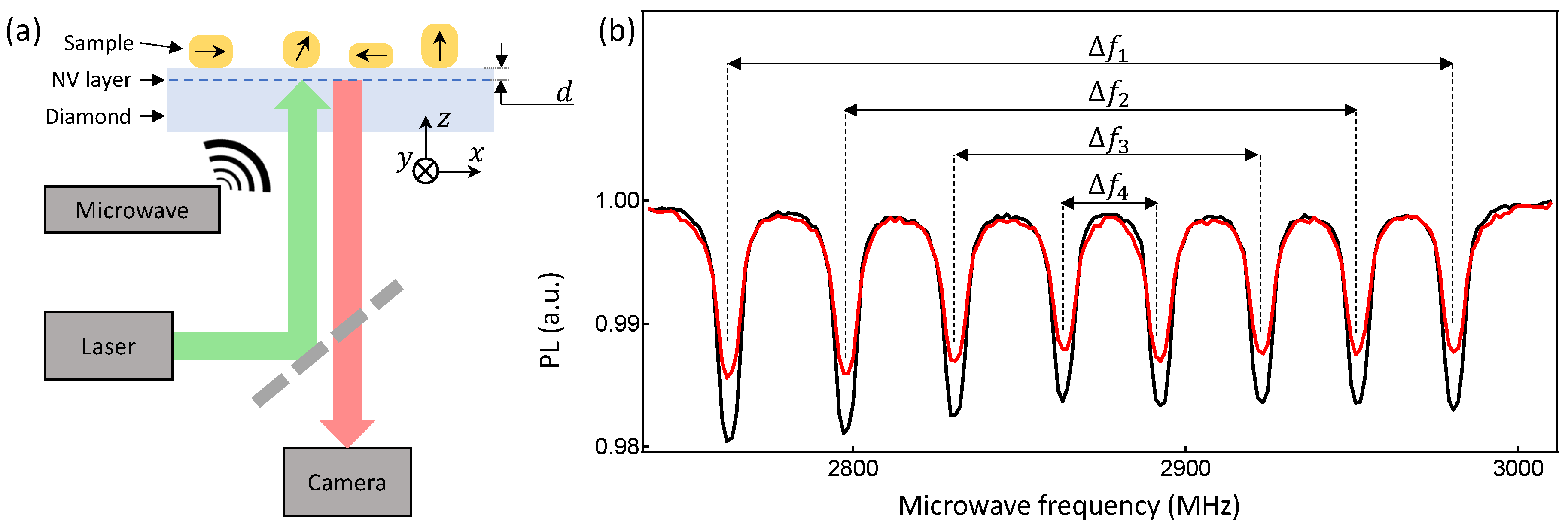
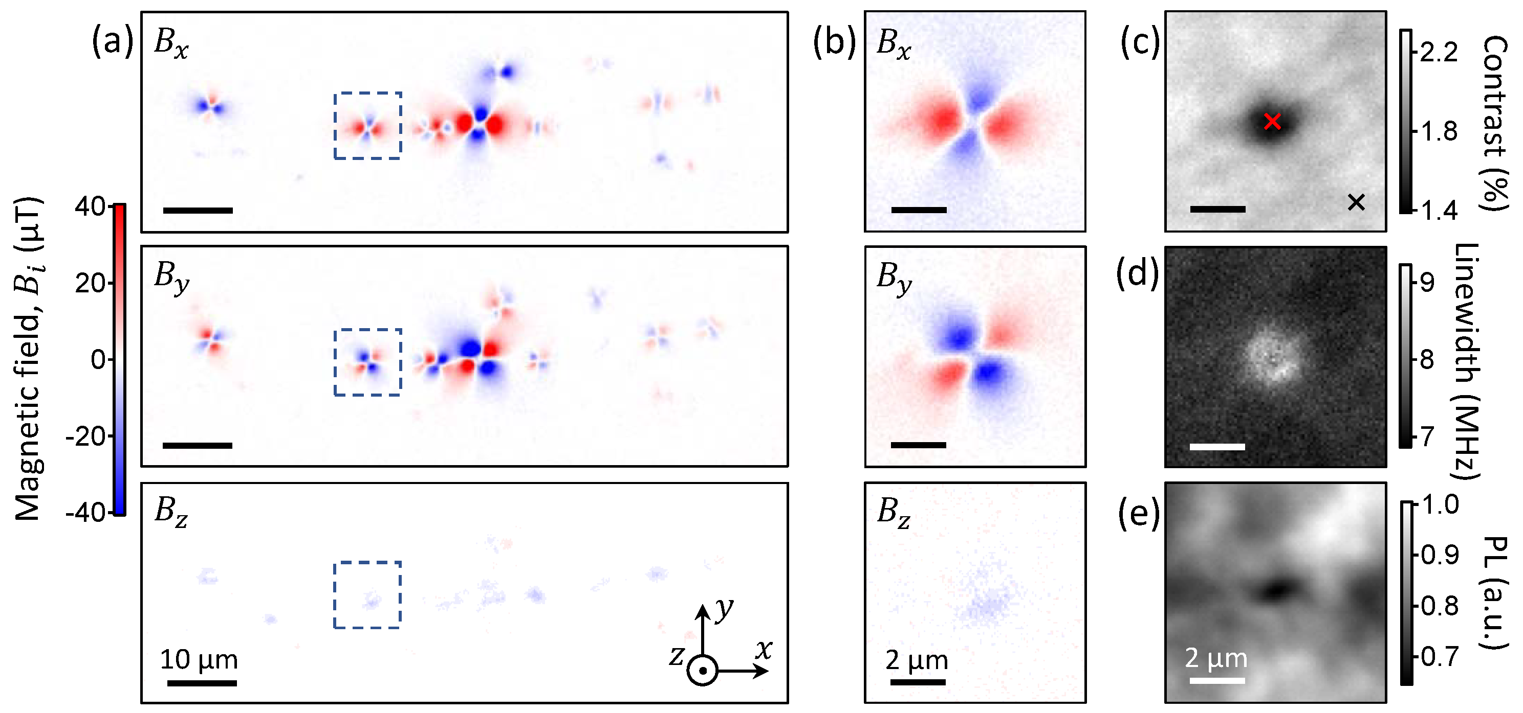
2. Experiment
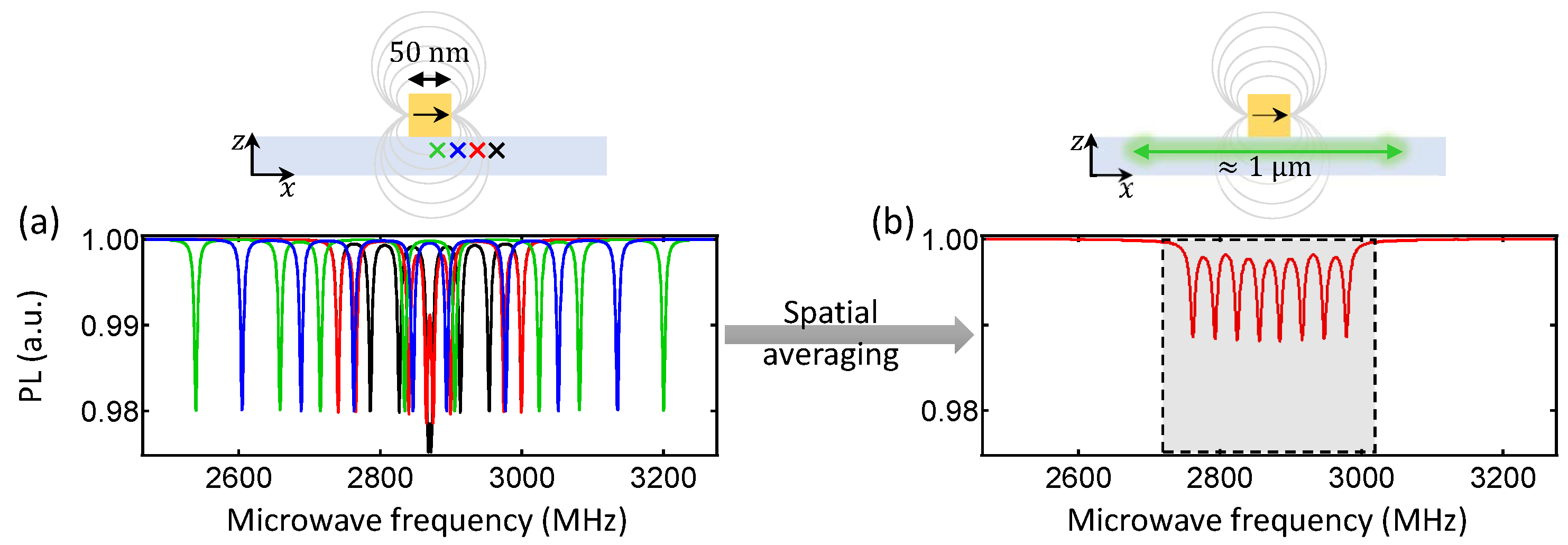
3. Modelling
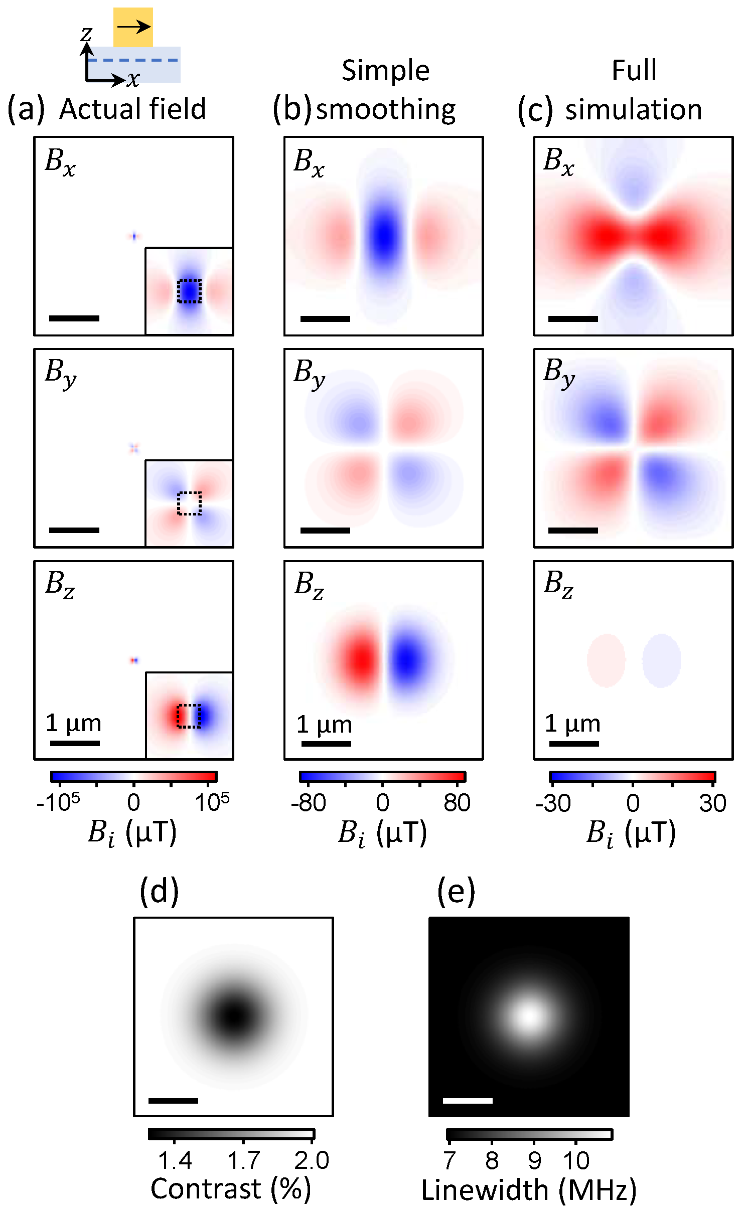
3.1. Nanoparticle with In-Plane Magnetisation
3.2. Distance Dependence
3.3. Nanoparticle with Out-of-Plane Magnetisation
4. Discussion
5. Conclusions
Acknowledgments
Author Contributions
Conflicts of Interest
References
- Doherty, M.W.; Manson, N.B.; Delaney, P.; Jelezko, F.; Wrachtrup, J.; Hollenberg, L.C.L. The nitrogen-vacancy colour centre in diamond. Phys. Rep. 2013, 528, 1–45. [Google Scholar] [CrossRef]
- Rondin, L.; Tetienne, J.P.; Hingant, T.; Roch, J.F.; Maletinsky, P.; Jacques, V. Magnetometry with nitrogen-vacancy defects in diamond. Rep. Prog. Phys. 2014, 77, 56503. [Google Scholar] [CrossRef] [PubMed]
- Schirhagl, R.; Chang, K.; Loretz, M.; Degen, C.L. Nitrogen-vacancy centers in diamond: Nanoscale sensors for physics and biology. Annu. Rev. Phys. Chem. 2014, 65, 83–105. [Google Scholar] [CrossRef] [PubMed]
- Taylor, J.M.; Cappellaro, P.; Childress, L.; Jiang, L.; Budker, D.; Hemmer, P.R.; Yacoby, A.; Walsworth, R.; Lukin, M.D. High-sensitivity diamond magnetometer with nanoscale resolution. Nat. Phys. 2008, 4, 29. [Google Scholar] [CrossRef]
- Degen, C.L. Scanning magnetic field microscope with a diamond single-spin sensor. Appl. Phys. Lett. 2008, 92, 2008–2010. [Google Scholar] [CrossRef]
- Dolde, F.; Fedder, H.; Doherty, M.W.; Nöbauer, T.; Rempp, F.; Balasubramanian, G.; Wolf, T.; Reinhard, F.; Hollenberg, L.C.L.; Jelezko, F.; et al. Electric-field sensing using single diamond spins. Nat. Phys. 2011, 7, 459–463. [Google Scholar] [CrossRef]
- Kucsko, G.; Maurer, P.C.; Yao, N.Y.; Kubo, M.; Noh, H.J.; Lo, P.K.; Park, H.; Lukin, M.D. Nanometre-scale thermometry in a living cell. Nature 2013, 500, 54–58. [Google Scholar] [CrossRef] [PubMed] [Green Version]
- Balasubramanian, G.; Chan, I.Y.; Kolesov, R.; Al-Hmoud, M.; Tisler, J.; Shin, C.; Kim, C.; Wojcik, A.; Hemmer, P.R.; Krueger, A.; et al. Nanoscale imaging magnetometry with diamond spins under ambient conditions. Nature 2008, 455, 648–651. [Google Scholar] [CrossRef] [PubMed]
- Maze, J.R.; Stanwix, P.L.; Hodges, J.S.; Hong, S.; Taylor, J.M.; Cappellaro, P.; Jiang, L.; Dutt, M.V.G.; Togan, E.; Zibrov, A.S.; et al. Nanoscale magnetic sensing with an individual electronic spin in diamond. Nature 2008, 455, 644–647. [Google Scholar] [CrossRef] [PubMed]
- Cole, J.H.; Hollenberg, L.C.L. Scanning quantum decoherence microscopy. Nanotechnology 2009, 20, 495401. [Google Scholar] [CrossRef] [PubMed]
- Balasubramanian, G.; Neumann, P.; Twitchen, D.; Markham, M.; Kolesov, R.; Mizuochi, N.; Isoya, J.; Achard, J.; Beck, J.; Tissler, J.; et al. Ultralong spin coherence time in isotopically engineered diamond. Nat. Mater. 2009, 8, 383–387. [Google Scholar] [CrossRef] [PubMed]
- Dréau, A.; Lesik, M.; Rondin, L.; Spinicelli, P.; Arcizet, O.; Roch, J.F.; Jacques, V. Avoiding power broadening in optically detected magnetic resonance of single NV defects for enhanced dc magnetic field sensitivity. Phys. Rev. B 2011, 84, 195204. [Google Scholar] [CrossRef]
- Maletinsky, P.; Hong, S.; Grinolds, M.S.; Hausmann, B.; Lukin, M.D.; Walsworth, R.L.; Loncar, M.; Yacoby, A. A robust scanning diamond sensor for nanoscale imaging with single nitrogen-vacancy centres. Nat. Nano 2011, 7, 320–324. [Google Scholar] [CrossRef] [PubMed] [Green Version]
- Rondin, L.; Tetienne, J.P.; Spinicelli, P.; Dal Savio, C.; Karrai, K.; Dantelle, G.; Thiaville, A.; Rohart, S.; Roch, J.F.; Jacques, V. Nanoscale magnetic field mapping with a single spin scanning probe magnetometer. Appl. Phys. Lett. 2012, 100, 153118. [Google Scholar] [CrossRef]
- Tetienne, J.P.; Hingant, T.; Kim, J.V.; Diez, L.H.; Adam, J.P.; Garcia, K.; Roch, J.F.; Rohart, S.; Thiaville, A.; Ravelosona, D.; et al. Nanoscale imaging and control of domain-wall hopping with a nitrogen-vacancy center microscope. Science 2014, 344, 1366–1369. [Google Scholar] [CrossRef] [PubMed]
- Pelliccione, M.; Jenkins, A.; Ovartchaiyapong, P.; Reetz, C.; Emmanuelidu, E.; Ni, N.; Bleszynski Jayich, A.C. Scanned probe imaging of nanoscale magnetism at cryogenic temperatures with a single-spin quantum sensor. Nat. Nanotechnol. 2016, 11, 700–705. [Google Scholar] [CrossRef] [PubMed]
- Thiel, L.; Rohner, D.; Ganzhorn, M.; Appel, P.; Neu, E.; Müller, B.; Kleiner, R.; Koelle, D.; Maletinsky, P. Quantitative nanoscale vortex-imaging using a cryogenic quantum magnetometer. Nat. Nanotechnol. 2016, 11, 677–681. [Google Scholar] [CrossRef] [PubMed]
- Steinert, S.; Dolde, F.; Neumann, P.; Aird, A.; Naydenov, B.; Balasubramanian, G.; Jelezko, F.; Wrachtrup, J. High sensitivity magnetic imaging using an array of spins in diamond. Rev. Sci. Instrum. 2010, 81, 043705. [Google Scholar] [CrossRef] [PubMed]
- Pham, L.M.; Le Sage, D.; Stanwix, P.L.; Yeung, T.K.; Glenn, D.; Trifonov, A.; Cappellaro, P.; Hemmer, P.R.; Lukin, M.D.; Park, H.; et al. Magnetic field imaging with nitrogen-vacancy ensembles. New J. Phys. 2011, 13, 045021. [Google Scholar] [CrossRef]
- Chipaux, M.; Tallaire, A.; Pezzagna, S.; Meijer, J.; Roch, J.F.; Jacques, V.; Debuisschert, T. Magnetic imaging with an ensemble of NV centers in diamond. Eur. Phys. J. D 2015, 69, 166. [Google Scholar] [CrossRef]
- Simpson, D.A.; Tetienne, J.P.; McCoey, J.M.; Ganesan, K.; Hall, L.T.; Petrou, S.; Scholten, R.E.; Hollenberg, L.C. Magneto-optical imaging of thin magnetic films using spins in diamond. Sci. Rep. 2016, 6, 22797. [Google Scholar] [CrossRef] [PubMed]
- Le Sage, D.; Arai, K.; Glenn, D.R.; DeVience, S.J.; Pham, L.M.; Rahn-Lee, L.; Lukin, M.D.; Yacoby, A.; Komeili, A.; Walsworth, R.L. Optical magnetic imaging of living cells. Nature 2013, 496, 486–489. [Google Scholar] [CrossRef] [PubMed] [Green Version]
- Fu, R.R.; Weiss, B.P.; Lima, E.A.; Harrison, R.J.; Bai, X.N.; Desch, S.J.; Ebel, D.S.; Suavet, C.; Wang, H.; Glenn, D.; et al. Solar nebula magnetic fields recorded in the Semarkona meteorite. Science 2014, 346, 1089–1092. [Google Scholar] [CrossRef] [PubMed] [Green Version]
- Glenn, D.R.; Lee, K.; Park, H.; Weissleder, R.; Yacoby, A.; Lukin, M.D.; Lee, H.; Walsworth, R.L.; Connolly, C.B. Single-cell magnetic imaging using a quantum diamond microscope. Nat. Methods 2015, 12, 736. [Google Scholar] [CrossRef] [PubMed]
- Tetienne, J.P.; Dontschuk, N.; Broadway, D.A.; Stacey, A.; Simpson, D.A.; Hollenberg, L.C.L. Quantum imaging of current flow in graphene. Sci. Adv. 2017, 3, e1602429. [Google Scholar] [CrossRef] [PubMed]
- Glenn, D.R.; Fu, R.R.; Kehayias, P.; Le Sage, D.; Lima, E.A.; Weiss, B.P.; Walsworth, R.L. Micrometer-scale magnetic imaging of geological samples using a quantum diamond microscope. Geochem. Geophys. Geosyst. 2017, 18, 3254–3267. [Google Scholar] [CrossRef]
- Maertz, B.J.; Wijnheijmer, A.P.; Fuchs, G.D.; Nowakowski, M.E.; Awschalom, D.D. Vector magnetic field microscopy using nitrogen vacancy centers in diamond. Appl. Phys. Lett. 2010, 96, 30–32. [Google Scholar] [CrossRef]
- Teraji, T. High-quality and high-purity homoepitaxial diamond (100) film growth under high oxygen concentration condition. J. Appl. Phys. 2015, 118, 115304. [Google Scholar] [CrossRef]
- Tetienne, J.P.; De Gille, R.; Broadway, D.; Teraji, T.; Lillie, S.; McCoey, J.; Dontschuk, N.; Hall, L.; Stacey, A.; Simpson, D.; et al. Spin properties of dense near-surface ensembles of nitrogen-vacancy centers in diamond. Phys. Rev. B 2018, 97, 085402. [Google Scholar] [CrossRef]
- Fávaro de Oliveira, F.; Momenzadeh, S.A.; Wang, Y.; Konuma, M.; Markham, M.; Edmonds, A.M.; Denisenko, A.; Wrachtrup, J. Effect of low-damage inductively coupled plasma on shallow nitrogen-vacancy centers in diamond. Appl. Phys. Lett. 2015, 107, 073107. [Google Scholar] [CrossRef]
- Lehtinen, O.; Naydenov, B.; Börner, P.; Melentjevic, K.; Müller, C.; McGuinness, L.P.; Pezzagna, S.; Meijer, J.; Kaiser, U.; Jelezko, F. Molecular dynamics simulations of shallow nitrogen and silicon implantation into diamond. Phys. Rev. B 2016, 93, 35202. [Google Scholar] [CrossRef]
- De Oliveira, F.F.; Antonov, D.; Wang, Y.; Neumann, P.; Momenzadeh, S.A.; Häußermann, T.; Pasquarelli, A.; Denisenko, A.; Wrachtrup, J. Tailoring spin defects in diamond. Nat. Commun. 2017, 8, 15409. [Google Scholar] [CrossRef] [PubMed]
- Coey, J.M.D. Magnetostatics. In Magnetism and Magnetic Materials; Cambridge University Press: Cambridge, UK, 2010; pp. 24–61. [Google Scholar]
- Tetienne, J.P.; Rondin, L.; Spinicelli, P.; Chipaux, M.; Debuisschert, T.; Roch, J.F.; Jacques, V. Magnetic-field-dependent photodynamics of single NV defects in diamond: An application to qualitative all-optical magnetic imaging. New J. Phys. 2012, 14, 103033. [Google Scholar] [CrossRef]
- Tisler, J.; Oeckinghaus, T.; Stöhr, R.J.; Kolesov, R.; Reuter, R.; Reinhard, F.; Wrachtrup, J. Single defect center scanning near-field optical microscopy on graphene. Nano Lett. 2013, 13, 3152–3156. [Google Scholar] [CrossRef] [PubMed]
- Maurer, P.C.; Maze, J.R.; Stanwix, P.L.; Jiang, L.; Gorshkov, A.V.; Zibrov, A.A.; Harke, B.; Hodges, J.S.; Zibrov, A.S.; Yacoby, A.; et al. Far-field optical imaging and manipulation of individual spins with nanoscale resolution. Nat. Phys. 2010, 6, 912–918. [Google Scholar] [CrossRef] [Green Version]
- Kleinsasser, E.E.; Stanfield, M.M.; Banks, J.K.Q.; Zhu, Z.; Li, W.D.; Acosta, V.M.; Watanabe, H.; Itoh, K.M.; Fu, K.M.C. High density NV sensing surface created via He+ ion implantation of 12C diamond. Appl. Phys. Lett. 2016, 8, 202401. [Google Scholar] [CrossRef]
- Steinert, S.; Ziem, F.; Hall, L.T.; Zappe, A.; Schweikert, M.; Götz, N.; Aird, A.; Balasubramanian, G.; Hollenberg, L.; Wrachtrup, J. Magnetic spin imaging under ambient conditions with sub-cellular resolution. Nat. Commun. 2013, 4, 1607. [Google Scholar] [CrossRef] [PubMed]
- DeVience, S.J.; Pham, L.M.; Lovchinsky, I.; Sushkov, A.O.; Bar-Gill, N.; Belthangady, C.; Casola, F.; Corbett, M.; Zhang, H.; Lukin, M.; et al. Nanoscale NMR spectroscopy and imaging of multiple nuclear species. Nat. Nanotechnol. 2015, 10, 129. [Google Scholar] [CrossRef] [PubMed]
- Simpson, D.A.; Ryan, R.G.; Hall, L.T.; Panchenko, E.; Drew, S.C.; Petrou, S.; Donnelly, P.S.; Mulvaney, P.; Hollenberg, L.C.L. Electron paramagnetic resonance microscopy using spins in diamond under ambient conditions. Nat. Commun. 2017, 8, 458. [Google Scholar] [CrossRef] [PubMed]
- Gong, C.; Li, L.; Li, Z.; Ji, H.; Stern, A.; Xia, Y.; Cao, T.; Bao, W.; Wang, C.; Wang, Y.; et al. Discovery of intrinsic ferromagnetism in 2D van der Waals crystals. Nature 2017, 546, 265. [Google Scholar] [CrossRef] [PubMed]
- Huang, B.; Clark, G.; Navarro-Moratalla, E.; Klein, D.R.; Cheng, R.; Seyler, K.L.; Zhong, D.; Schmidgall, E.; McGuire, M.A.; Cobden, D.H.; et al. Layer-dependent Ferromagnetism in a van der Waals Crystal down to the Monolayer Limit. Nature 2017, 546, 270. [Google Scholar] [CrossRef] [PubMed]
- Magda, G.Z.; Jin, X.; Hagymási, I.; Vancsó, P.; Osváth, Z.; Nemes-Incze, P.; Hwang, C.; Biró, L.P.; Tapasztó, L. Room-temperature magnetic order on zigzag edges of narrow graphene nanoribbons. Nature 2014, 514, 608. [Google Scholar] [CrossRef] [PubMed]
- Luxa, J.; Jankovský, O.; Sedmidubský, D.; Medlín, R.; Maryško, M.; Pumera, M.; Sofer, Z. Origin of exotic ferromagnetic behavior in exfoliated layered transition metal dichalcogenides MoS2 and WS2. Nanoscale 2016, 8, 1960–1967. [Google Scholar] [CrossRef] [PubMed]
- Radhakrishnan, S.; Das, D.; Samanta, A.; Reyes, C.A.D.L.; Deng, L.; Alemany, L.B.; Weldeghiorghis, T.K.; Khabashesku, V.N.; Kochat, V.; Jin, Z.; et al. Fluorinated h-BN as a magnetic semiconductor. Sci. Adv. 2017, 3, e1700842. [Google Scholar] [CrossRef] [PubMed]
- Lovchinsky, I.; Sanchez-Yamagishi, J.D.; Urbach, E.K.; Choi, S.; Fang, S.; Andersen, T.I.; Watanabe, K.; Taniguchi, T.; Bylinskii, A.; Kaxiras, E.; et al. Magnetic resonance spectroscopy of an atomically thin material using a single-spin qubit. Science 2017, 355, 503–507. [Google Scholar] [CrossRef] [PubMed]


© 2018 by the authors. Licensee MDPI, Basel, Switzerland. This article is an open access article distributed under the terms and conditions of the Creative Commons Attribution (CC BY) license (http://creativecommons.org/licenses/by/4.0/).
Share and Cite
Tetienne, J.-P.; Broadway, D.A.; Lillie, S.E.; Dontschuk, N.; Teraji, T.; Hall, L.T.; Stacey, A.; Simpson, D.A.; Hollenberg, L.C.L. Proximity-Induced Artefacts in Magnetic Imaging with Nitrogen-Vacancy Ensembles in Diamond. Sensors 2018, 18, 1290. https://doi.org/10.3390/s18041290
Tetienne J-P, Broadway DA, Lillie SE, Dontschuk N, Teraji T, Hall LT, Stacey A, Simpson DA, Hollenberg LCL. Proximity-Induced Artefacts in Magnetic Imaging with Nitrogen-Vacancy Ensembles in Diamond. Sensors. 2018; 18(4):1290. https://doi.org/10.3390/s18041290
Chicago/Turabian StyleTetienne, Jean-Philippe, David A. Broadway, Scott E. Lillie, Nikolai Dontschuk, Tokuyuki Teraji, Liam T. Hall, Alastair Stacey, David A. Simpson, and Lloyd C. L. Hollenberg. 2018. "Proximity-Induced Artefacts in Magnetic Imaging with Nitrogen-Vacancy Ensembles in Diamond" Sensors 18, no. 4: 1290. https://doi.org/10.3390/s18041290