
Micrometer Sized Hexagonal Chromium Selenide Flakes for Cryogenic Temperature Sensors

 , , , ,
  , ,
, ,  and
and
Abstract
:1. Introduction
2. Materials and Methods
3. Results and Discussion
4. Conclusions
Author Contributions
Funding
Institutional Review Board Statement
Informed Consent Statement
Data Availability Statement
Conflicts of Interest
References
- Pekola, J.P. Towards quantum thermodynamics in electronic circuits. Nat. Phys. 2015, 11, 118–123. [Google Scholar] [CrossRef] [Green Version]
- Giazotto, F.; Martínez-Pérez, M.J. The josephson heat interferometer. Nature 2012, 492, 401–405. [Google Scholar] [CrossRef] [PubMed] [Green Version]
- Quan, H.T.; Zhang, P.; Sun, C.P. Quantum heat engine with multilevel quantum systems. Phys. Rev. E 2005, 72, 056110. [Google Scholar] [CrossRef] [Green Version]
- Hicks, L.D.; Dresselhaus, M.S. Effect of quantum-well structures on the thermoelectric figure of merit. Phys. Rev. B 1993, 47, 12727–12731. [Google Scholar] [CrossRef]
- Harman, T.C.; Taylor, P.J.; Walsh, M.P.; LaForge, B.E. Quantum dot superlattice thermoelectric materials and devices. Science 2002, 297, 2229–2232. [Google Scholar] [CrossRef] [PubMed] [Green Version]
- Yeager, C.J.; Courts, S.S. A review of cryogenic thermometry and common temperature sensors. IEEE Sens. J. 2001, 1, 352–360. [Google Scholar] [CrossRef]
- Kjekshus, A.; Pearson, W.B. Phases with the nickel arsenide and closely-related structures. Prog. Solid State Chem. 1964, 1, 83–174. [Google Scholar] [CrossRef]
- Corliss, L.M.; Elliott, N.; Hastings, J.M.; Sass, R.L. Magnetic structure of chromium selenide. Phys. Rev. 1961, 122, 1402–1406. [Google Scholar] [CrossRef]
- Zhang, T.; Su, X.; Yan, Y.; Liu, W.; You, Y.; Xie, H.; Yang, D.; Uher, C.; Tang, X. Structure and thermoelectric properties of 2D Cr2Se3−3xS3x solid solutions. J. Mater. Chem. C 2018, 6, 836–846. [Google Scholar] [CrossRef]
- Mahan, G.; Sales, B.; Sharp, J. Thermoelectric materials: New approaches to an old problem. Phys. Today 1997, 50, 42–47. [Google Scholar] [CrossRef]
- Ramaraj, S.; Mani, S.; Chen, S.-M.; Palanisamy, S.; Velusamy, V.; Hall, J.M.; Chen, T.-W.; Tseng, T.-W. Hydrothermal synthesis of Cr2Se3 hexagons for sensitive and low-level detection of 4-nitrophenol in water. Sci. Rep. 2018, 8, 4839. [Google Scholar] [CrossRef] [Green Version]
- Zhang, T.; Su, X.; Yan, Y.; Liu, W.; Hu, T.; Zhang, C.; Zhang, Z.; Tang, X. Enhanced thermoelectric properties of codoped Cr2Se3: The distinct roles of transition metals and S. ACS Appl. Mater. Interfaces 2018, 10, 22389–22400. [Google Scholar] [CrossRef] [PubMed]
- Guo, Q.; Berthebaud, D.; Ueda, J.; Tanabe, S.; Miyoshi, A.; Maeda, K.; Mori, T. Facile p–n control, and magnetic and thermoelectric properties of chromium selenides Cr2+xSe3. J. Mater. Chem. C 2019, 7, 8269–8276. [Google Scholar] [CrossRef]
- Li, B.; Wan, Z.; Wang, C.; Chen, P.; Huang, B.; Cheng, X.; Qian, Q.; Li, J.; Zhang, Z.; Sun, G.; et al. Van der waals epitaxial growth of air-stable CrSe2 nanosheets with thickness-tunable magnetic order. Nat. Mater. 2021, 20, 818–825. [Google Scholar] [CrossRef] [PubMed]
- Zhang, Y.; Chu, J.; Yin, L.; Shifa, T.A.; Cheng, Z.; Cheng, R.; Wang, F.; Wen, Y.; Zhan, X.; Wang, Z.; et al. Ultrathin magnetic 2D single-crystal CrSe. Adv. Mater. 2019, 31, e1900056. [Google Scholar] [CrossRef] [PubMed]
- Buruiana, A.T.; Sava, F.; Matei, E.; Zgura, I.; Burdusel, M.; Mihai, C.; Velea, A. Simple and clean method for obtaining Sn nanoparticles for hydrophobic coatings. Mater. Lett. 2020, 278, 128419. [Google Scholar] [CrossRef]
- Mardare, D.; Luca, D.; Teodorescu, C.-M.; Macovei, D. On the hydrophilicity of nitrogen-doped TiO2 thin films. Surf. Sci. 2007, 601, 4515–4520. [Google Scholar] [CrossRef]
- Cui, F.; Zhao, X.; Xu, J.; Tang, B.; Shang, Q.; Shi, J.; Huan, Y.; Liao, J.; Chen, Q.; Hou, Y.; et al. Controlled growth and thickness-dependent conduction-type transition of 2D ferrimagnetic Cr2S3 semiconductors. Adv. Mater. 2020, 32, e1905896. [Google Scholar] [CrossRef] [PubMed]
- Agostinelli, E.; Battistoni, C.; Fiorani, D.; Mattogno, G.; Nogues, M. An XPS study of the electronic structure of the ZnxCd1−xCr2 (X = S, Se) spinel system. J. Phys. Chem. Solids 1989, 50, 269–272. [Google Scholar] [CrossRef]
- Gupta, P.; Bhargava, R.; Das, R.; Poddar, P. Static and dynamic magnetic properties and effect of surface chemistry on the morphology and crystallinity of DyCrO3 nanoplatelets. RSC Adv. 2013, 3, 26427. [Google Scholar] [CrossRef]
- Toh, R.J.; Sofer, Z.; Pumera, M. Catalytic properties of group 4 transition metal dichalcogenides (MX2; M = Ti, Zr, Hf; X = S, Se, Te). J. Mater. Chem. A 2016, 4, 18322–18334. [Google Scholar] [CrossRef]
- Wagner, C.D.; Davis, L.E.; Zeller, M.V.; Taylor, J.A.; Raymond, R.H.; Gale, L.H. Empirical atomic sensitivity factors for quantitative analysis by electron spectroscopy for chemical analysis. Surf. Interface Anal. 1981, 3, 211–225. [Google Scholar] [CrossRef]
- Shinotsuka, H.; Tanuma, S.; Powell, C.J.; Penn, D.R. Calculations of electron inelastic mean free paths. X. Data for 41 elemental solids over the 50 EV to 200 KeV range with the relativistic full penn algorithm. Surf. Interface Anal. 2015, 47, 871–888. [Google Scholar] [CrossRef]
- Monea, B.; Ionete, E.; Spiridon, S.; Leca, A.; Stanciu, A.; Petre, E.; Vaseashta, A. Single wall carbon nanotubes based cryogenic temperature sensor platforms. Sensors 2017, 17, 2071. [Google Scholar] [CrossRef] [PubMed] [Green Version]
- Sambles, J.R.; Elsom, K.C.; Jarvis, D.J. The electrical resistivity of gold films. Philos. Trans. R. Soc. Lond. Ser. A Math. Phys. Sci. 1982, 304, 365–396. [Google Scholar] [CrossRef]
- Clark, A.F.; Childs, G.E.; Wallace, G.H. Electrical resistivity of some engineering alloys at low temperatures. Cryogenics 1970, 10, 295–305. [Google Scholar] [CrossRef]
- Oliva, A.I.; Lugo, J.M.; Gurubel-Gonzalez, R.A.; Centeno, R.J.; Corona, J.E.; Avilés, F. Temperature coefficient of resistance and thermal expansion coefficient of 10-Nm thick gold films. Thin Solid Films 2017, 623, 84–89. [Google Scholar] [CrossRef]
- Singh, B.; Surplice, N.A. The electrical resistivity and resistance-temperature characteristics of thin titanium films. Thin Solid Films 1972, 10, 243–253. [Google Scholar] [CrossRef]
- Rogalski, A. Infrared Detectors; CRC Press: Boca Raton, FL, USA, 2020; ISBN 9780367577094. [Google Scholar]
- Dasd Bat’ko, I.; Somora, M.; Vanický, D.; Flachbart, K. RuO2-based thick-film resistors as high sensitivity thermometers for millikelvin temperatures. Cryogenics 1992, 32, 1167–1168. [Google Scholar] [CrossRef]
- Yotsuya, T.; Kakehi, Y.; Ishida, T. Thin film temperature sensor for cryogenic region with small magnetoresistance. Cryogenics 2011, 51, 546–549. [Google Scholar] [CrossRef]
- Yotsuya, T.; Yoshitake, M.; Yamamoto, J. New type cryogenic thermometer using sputtered Zr-N films. Appl. Phys. Lett. 1987, 51, 235–237. [Google Scholar] [CrossRef]
- Mitin, V.F.; McDonald, P.C.; Pavese, F.; Boltovets, N.S.; Kholevchuk, V.V.; Nemish, I.Y.; Basanets, V.V.; Dugaev, V.K.; Sorokin, P.V.; Konakova, R.V.; et al. Ge-on-GaAs film resistance thermometers for cryogenic applications. Cryogenics 2007, 47, 474–482. [Google Scholar] [CrossRef]
- Nguyen, T.; Tavakoli, A.; Triqueneaux, S.; Swami, R.; Ruhtinas, A.; Gradel, J.; Garcia-Campos, P.; Hasselbach, K.; Frydman, A.; Piot, B.; et al. Niobium nitride thin films for very low temperature resistive thermometry. J. Low Temp. Phys. 2019, 197, 348–356. [Google Scholar] [CrossRef] [Green Version]
- Griffin, E.L.; Mochel, J.M. Low temperature, thin film NiCr thermometers. Rev. Sci. Instrum. 1974, 45, 1265–1267. [Google Scholar] [CrossRef]
- Obukhov, S.A. New type of cryogenic semiconductor resistance thermometer. Cryogenics 1994, 34, 237–240. [Google Scholar] [CrossRef]
- Blagg, K.; Allen, P.; Lu, T.-M.; Lilly, M.P.; Singh, M. Focused ion beam deposited carbon-platinum nanowires for cryogenic resistive thermometry. Carbon 2020, 169, 482–487. [Google Scholar] [CrossRef]


| y0 | x0 | A1 | t1 | A2 | t2 | A3 | t3 | R2 |
|---|---|---|---|---|---|---|---|---|
| 11.14 | 7.74 | 151.42 | 4.37 | 157.22 | 1.46 | 40.8 | 23 | 0.99998 |
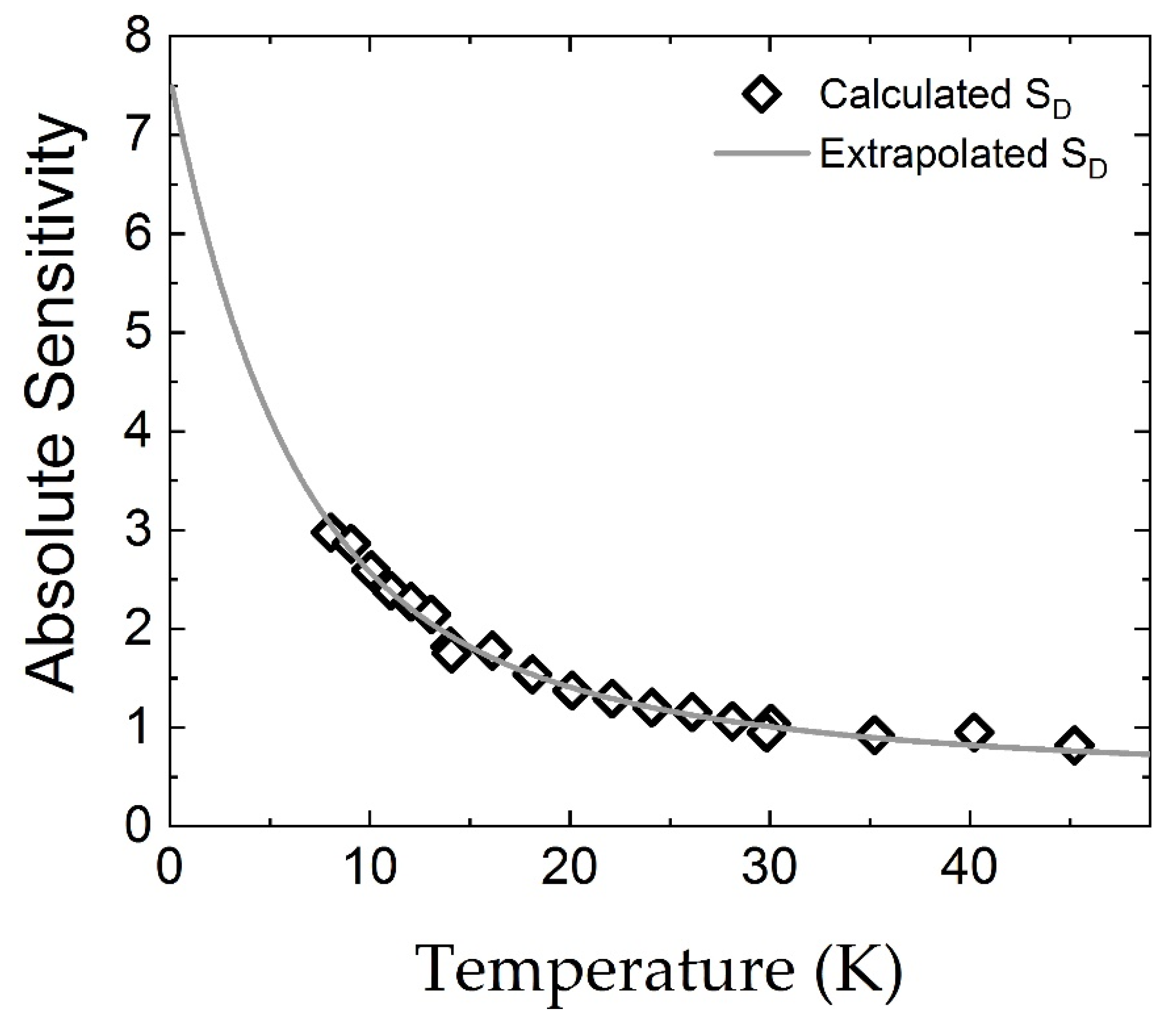
| Material | Temperature Range (K) | Sensitivity | Cr-Se Sensitivity (This Work) |
|---|---|---|---|
| RuO2 [30] | 0.1–1.6 | 2.4–0.25 | 7.49–6.16 |
| CrN [31] | 1.8–300 | 2–1 | 6.00–0.58 |
| ZrN [32] | 2–300 | 0.54–0.14 | 5.80–0.58 |
| Ge-GaAs [33] | 0.03–500 | 4.3–0.1 | 7.56–0.58 |
| NbN [34] | 0.1–300 | 3.7–0.7 | 7.49–0.58 |
| NiCr [35] | 0.4–4 | 4.7–0.1 | 7.19–4.62 |
| InSb [36] | 0.01–10 | 10–0.1 | 7.60–2.57 |
| FIB C-Pt [37] | 0.1–8 | 14.88–0.001 | 7.49–3.06 |
Publisher’s Note: MDPI stays neutral with regard to jurisdictional claims in published maps and institutional affiliations. |
© 2021 by the authors. Licensee MDPI, Basel, Switzerland. This article is an open access article distributed under the terms and conditions of the Creative Commons Attribution (CC BY) license (https://creativecommons.org/licenses/by/4.0/).
Share and Cite
Buruiana, A.-T.; Sava, F.; Iacob, N.; Matei, E.; Bocirnea, A.E.; Onea, M.; Galca, A.-C.; Mihai, C.; Velea, A.; Kuncser, V. Micrometer Sized Hexagonal Chromium Selenide Flakes for Cryogenic Temperature Sensors. Sensors 2021, 21, 8084. https://doi.org/10.3390/s21238084
Buruiana A-T, Sava F, Iacob N, Matei E, Bocirnea AE, Onea M, Galca A-C, Mihai C, Velea A, Kuncser V. Micrometer Sized Hexagonal Chromium Selenide Flakes for Cryogenic Temperature Sensors. Sensors. 2021; 21(23):8084. https://doi.org/10.3390/s21238084
Chicago/Turabian StyleBuruiana, Angel-Theodor, Florinel Sava, Nicusor Iacob, Elena Matei, Amelia Elena Bocirnea, Melania Onea, Aurelian-Catalin Galca, Claudia Mihai, Alin Velea, and Victor Kuncser. 2021. "Micrometer Sized Hexagonal Chromium Selenide Flakes for Cryogenic Temperature Sensors" Sensors 21, no. 23: 8084. https://doi.org/10.3390/s21238084