
0.3-Volt Rail-to-Rail DDTA and Its Application in a Universal Filter and Quadrature Oscillator


1
Department of Microelectronics, Brno University of Technology, Technická 10, 601 90 Brno, Czech Republic
2
Faculty of Biomedical Engineering, Czech Technical University in Prague, Nám. Sítná 3105, 166 36 Kladno, Czech Republic
3
Department of Telecommunications Engineering, School of Engineering, King Mongkut’s Institute of Technology Ladkrabang, Bangkok 10520, Thailand
4
Department of Electrical Engineering, Czestochowa University of Technology, 42-201 Czestochowa, Poland
5
Department of Electrical Engineering, Brno University of Defence, Kounicova 65, 662 10 Brno, Czech Republic
*
Author to whom correspondence should be addressed.
Sensors 2022, 22(7), 2655; https://doi.org/10.3390/s22072655
Submission received: 24 February 2022
/
Revised: 23 March 2022
/
Accepted: 26 March 2022
/
Published: 30 March 2022
(This article belongs to the Section Electronic Sensors)
Abstract
:This paper presents the extremely low-voltage supply of the CMOS structure of a differential difference transconductance amplifier (DDTA). With a 0.3-volt supply voltage, the circuit offers rail-to-rail operational capability. The circuit is designed for low-frequency biomedical and sensor applications, and it consumes 357.4 nW of power. Based on two DDTAs and two grounded capacitors, a voltage-mode universal filter and quadrature oscillator are presented as applications. The universal filter possesses high-input impedance and electronic tuning ability of the natural frequency in the range of tens up to hundreds of Hz. The total harmonic distortion (THD) for the band-pass filter was 0.5% for 100 mVpp @ 84.47 Hz input voltage. The slight modification of the filter yields a quadrature oscillator. The condition and the frequency of oscillation are orthogonally controllable. The frequency of oscillation can also be controlled electronically. The THD for a 67 Hz oscillation frequency was around 1.2%. The circuit is designed and simulated in a Cadence environment using 130 nm CMOS technology from United Microelectronics Corporation (UMC). The simulation results confirm the performance of the designed circuits.
1. Introduction
In recent years, extremely low-voltage operation capability and low-power consumption became inevitable requirements in modern, battery-operated, portable electronics and self-powered systems. In modern nanoscale complementary metal–oxide–semiconductor (CMOS) technologies, scaling the power supply voltage sustains the reliability and performance improvement of digital circuits; however, it causes performance degradation in the analog part. This poses a continual challenge for analog circuit designers to maintain acceptable performance for applications and systems-on-chip. The main impact of reducing the voltage supply on analog circuit performance, such as an operational amplifier (Op-Amp) or transconductance amplifier (TA or OTA), is the reduced input voltage swing, the transconductance value, and the voltage gain. A conventional design technique used to increase the input voltage swing is rail-to-rail circuits composed of both PMOS and NMOS differential pairs. However, these circuits are complex due to the additional differential pair, current branches, and circuitry used to maintain constant transconductance over the whole input voltage range. Therefore, non-conventional techniques, such as bulk-driven (BD) [1,2,3,4,5,6,7,8,9,10,11,12,13,14], floating-gate (FG), and quasi-floating-gate (QFG) [15,16], are suitable candidates for circuits operating with low supply voltages. They may reduce the threshold voltage or even remove it from the signal path, resulting in an extended input voltage range. Multiple-input MOS transistor (MI-MOST) is an alternative technique to the FG. However, unlike the FG, the MI-MOST: (a) does not need two polysilicon technologies; hence, it can be implemented in any standard CMOS technology; (b) it can process both AC and DC signals; and (c) there is no gate floating, and hence no issue associated with removing the initial charge trapped as in the case of FG. The multiple-input can be applied to the gate, to the bulk, or to their combination [17,18,19,20,21,22,23,24,25,26,27]. From the realization point of view, analog filter applications with MI-MOST may reduce the count of needed active devices [17,18,19,20,21,22,23,24,28,29]. This leads to simplified filter circuitry and reduced power consumption and chip area.
The universal filter and oscillator are important blocks for analog signal processing. Their applications include communication, control, and instrumentation systems [30,31,32]. Biquadratic filters and oscillators can be applied to biomedical systems [33,34,35]. Therefore, low-voltage supply and low-power consumption are mainly considered for these applications.
The differential difference transconductance amplifier (DDTA) is a useful analog block for filter applications [36,37,38,39,40]. It combines the features of a differential difference amplifier (DDA) with unity gain, like addition and subtraction voltage ability, high-input impedance, a low number of components, and the advantages of a operational transconductance amplifier (OTA), such as electronic tuning ability and simple circuitry. There are DDTA-based universal filters and oscillators available in the literature [36,37,38,39,40]. However, these DDTAs are not suitable for extremely low-voltage supply (i.e., ≤0.3 V) applications. Their structures are standard; hence, reducing their voltage supply leads to significant performance degradation, for instance a reduced input voltage swing. Focusing on recently published universal filters and/or oscillators [41,42,43,44,45,46,47], only the circuit in [48] can work with sub-volt supply (±0.3 V) and low-power consumption (5.77 µW).
Therefore, this paper presents an innovative CMOS structure for DDTA capable of working under a 0.3 V supply voltage with a rail-to-rail input voltage swing without degrading the other circuit’s performance. As an application of DDTA, a multiple-input, multiple-output (MIMO) universal filter is presented. The filter employs two DDTAs and two grounded capacitors. A variety of filter responses can be obtained by suitably applying the input signal and suitably choosing the output terminal. The natural frequency of filter responses can be electronically controlled. The proposed universal filter has also been modified to work as a quadrature oscillator. The frequency of oscillation can be controlled electronically. The proposed universal filter and quadrature oscillator can be applied to biomedical and sensor systems due to their extremely low voltage supply and low power consumption.
2. DDTA and Its CMOS Structure
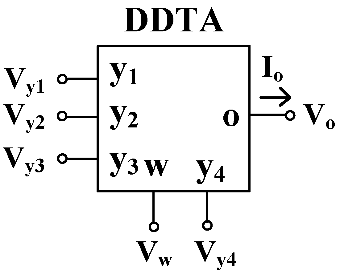
The symbol of the DDTA is shown in Figure 1. In the ideal case, this active component is described by the following equations:
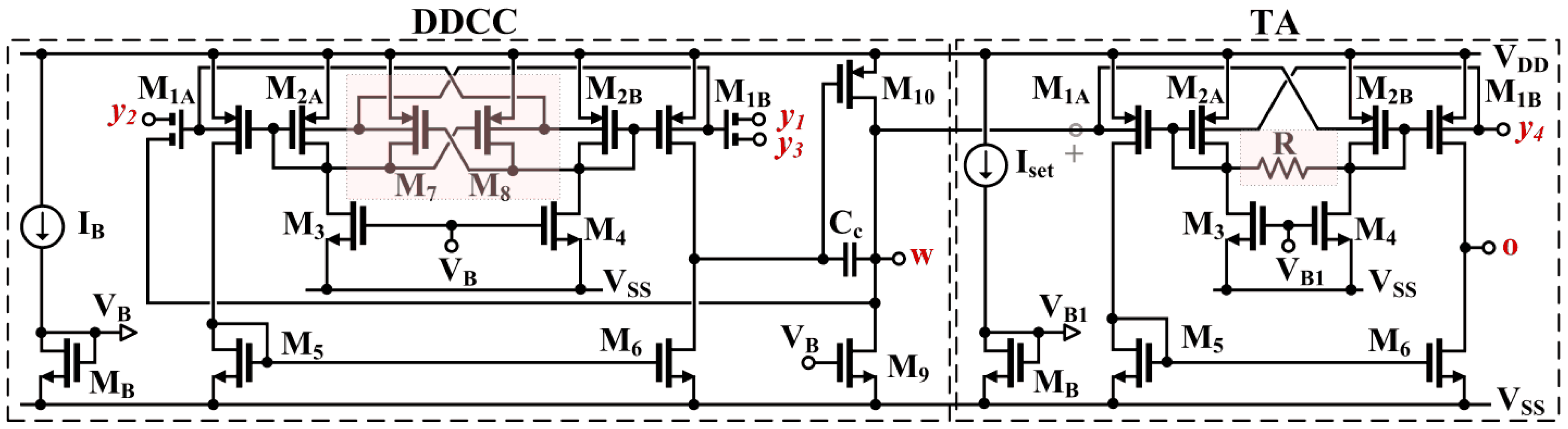
The CMOS structure of the proposed DDTA is shown in Figure 2. The circuit consists of two main blocks, namely, the differential-difference amplifier operating in a unity feedback configuration, thus forming a differential-difference current conveyor (DDCC), and the transconductance amplifier (TA). Both circuits are based on non-tailed differential amplifiers [1], which allow for operation in an ultra-low-voltage environment with rail-to-rail input swing.
The DDCC block consists of two stages, the input differential amplifier, M1–M6, and the class-A output stage, M9–M10. The capacitance CC is used for frequency compensation. Its value can be calculated in the same way as that for a two-stage operational amplifier. The input stage of the DDCC circuit can be seen as a non-tailed differential pair with an additional partial positive feedback (PPF) circuit. The solution, first presented in [2] and experimentally validated in [3], has been adopted here. The transistors, M7 and M8, generate negative conductances, -gm7 and -gm8, which partially compensate for the positive conductances of the diode-connected transistors, M2A,B (≈gm2), thus increasing the resistances at the gate-drain nodes of these transistors, and consequently the voltage gain from inputs to the gate terminals of M1A,B. This improves the overall transconductance and voltage gain of the first stage.
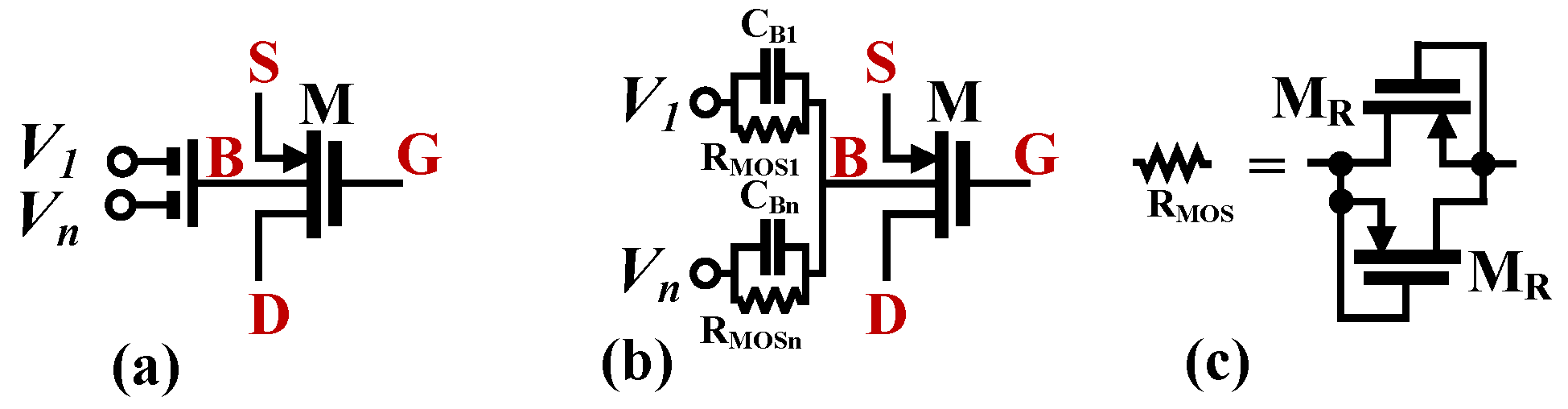
In the proposed realization, the input transistors M1A,B have been replaced by bulk-driven MI-MOST transistors. The symbol and CMOS realization of these devices are shown in Figure 3. This approach allows design simplification and the decreasing of the total dissipation power by removing one differential stage of the conventional DDCC. This is the result of the fact that summation of input signals is realized using the passive voltage divider/summing circuit composed of the capacitances CBi (see Figure 3b). The capacitances are shunted by large resistances, RMOSi, that allow proper DC biasing of the bulk terminals of M1A,B. The resistors are realized as the antiparallel connection of two MOS transistors operating in a cutoff region, as shown in Figure 3c.
The low-frequency open-loop voltage gain of the DDCC, from one differential input, with the second input grounded for AC signals, can be expressed as follows:
where Gm is the transconductance of the input differential stage given by:
where β is the voltage gain of the input capacitive divider, equal to ½ if all capacitances CBi are equal to each other and the input capacitance of the MOS transistor from its bulk terminal can be neglected. The factor m represents the absolute value of the ratio of negative to positive conductances at the gate/drain nodes of M2A,B:
Note that the transconductance Gm as well as the voltage gain Avo tend to infinity, as m tends to unity, namely, when the negative conductances generated by M7 and M8 fully compensate the positive conductances of M2, thus leading to infinite voltage gain from inputs to the drain/gate nodes of M2A,B. However, when the difference between gm2 and gm7,8 is decreasing, namely when m is increasing to unity, then the circuit sensitivity to transistor mismatch is increasing as well, which limits the maximum value of m. The second limitation is associated with the location of the parasitic pole associated with the PPF circuit, which is given by the formula
where C∑ is the total capacitance associated with the gate/drain nodes of M2A,B. Note that the frequency of this pole decreases with increasing m, namely, as the total resistance at the gate/drain nodes of M2 increases with increasing positive feedback. For stable operation, the pole should be located well above the GBW product of the internal DDA, which is
In view of the above considerations, the output signal at the W terminal for low frequencies can be expressed as
Note that accuracy of this function is improved thanks to the impact of the PPF, which enlarges the low-frequency voltage gain Avo. The 3 dB frequency of this function is approximately equal to ωGBW. The low-frequency output resistance at the W terminal is given as follows:
Thus, the resistance routW is also improved (decreased) thanks to the larger value of Avo.
The second block of the proposed DDTA is the linear transconductance amplifier, TA. The circuit applied here was first proposed and validated experimentally in [4]. It can be considered as a non-tailed BD pair [1], linearized with an additional linear resistance R, which significantly improves the linearity of the circuit. Thanks to its non-tailed architecture, the circuit can operate from a very low-voltage supply.
Assuming that transistor MB is identical with M3 and M4, the DC transfer characteristic of the TA in Figure 2 can be described by the formula [4]
where
and np is the subthreshold slope factor for a p-channel MOS, UT is the thermal potential, and η = (np − 1) = gmb1,2/gm1,2 is the bulk-to-gate transconductance ratio for transistors M1 and M2.
As it was shown in [4], if the following condition holds
then the circuit exhibits an optimum linearity. However, even for the non-optimal case, the linearity of Equation (9) is much better than for the original circuit without the resistance, R; therefore, the TA can be tuned using the current source Iset, while still maintaining good linearity of its transfer characteristic.
The small-signal transconductance gm of the TA in the general case is
thus, in the optimum case, (R = 1/gm1,2), it is equal to 4gmb1,2/3.
3. Proposed Applications
3.1. Proposed Universal Filter
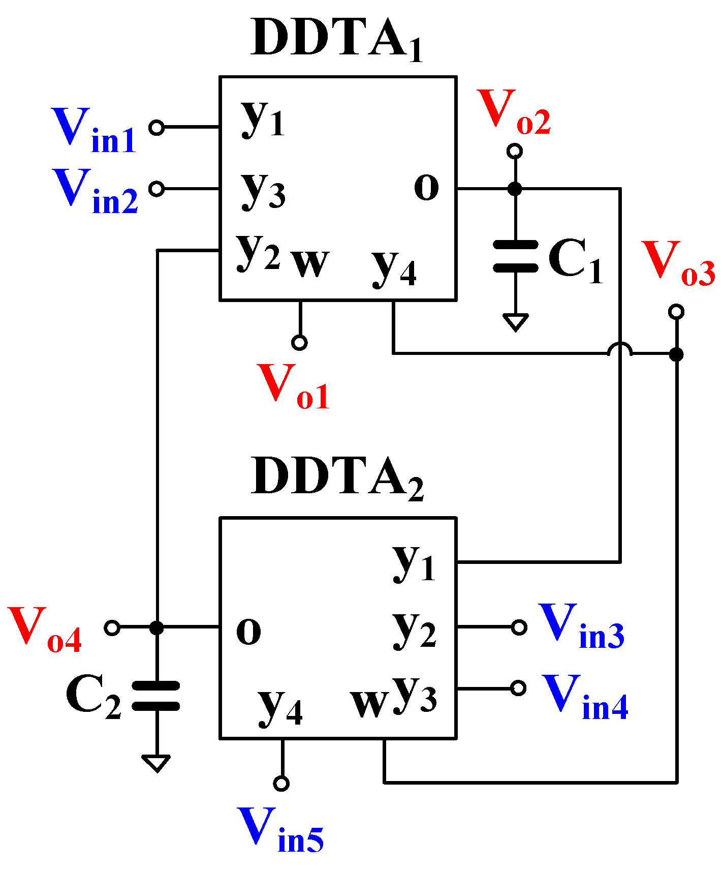
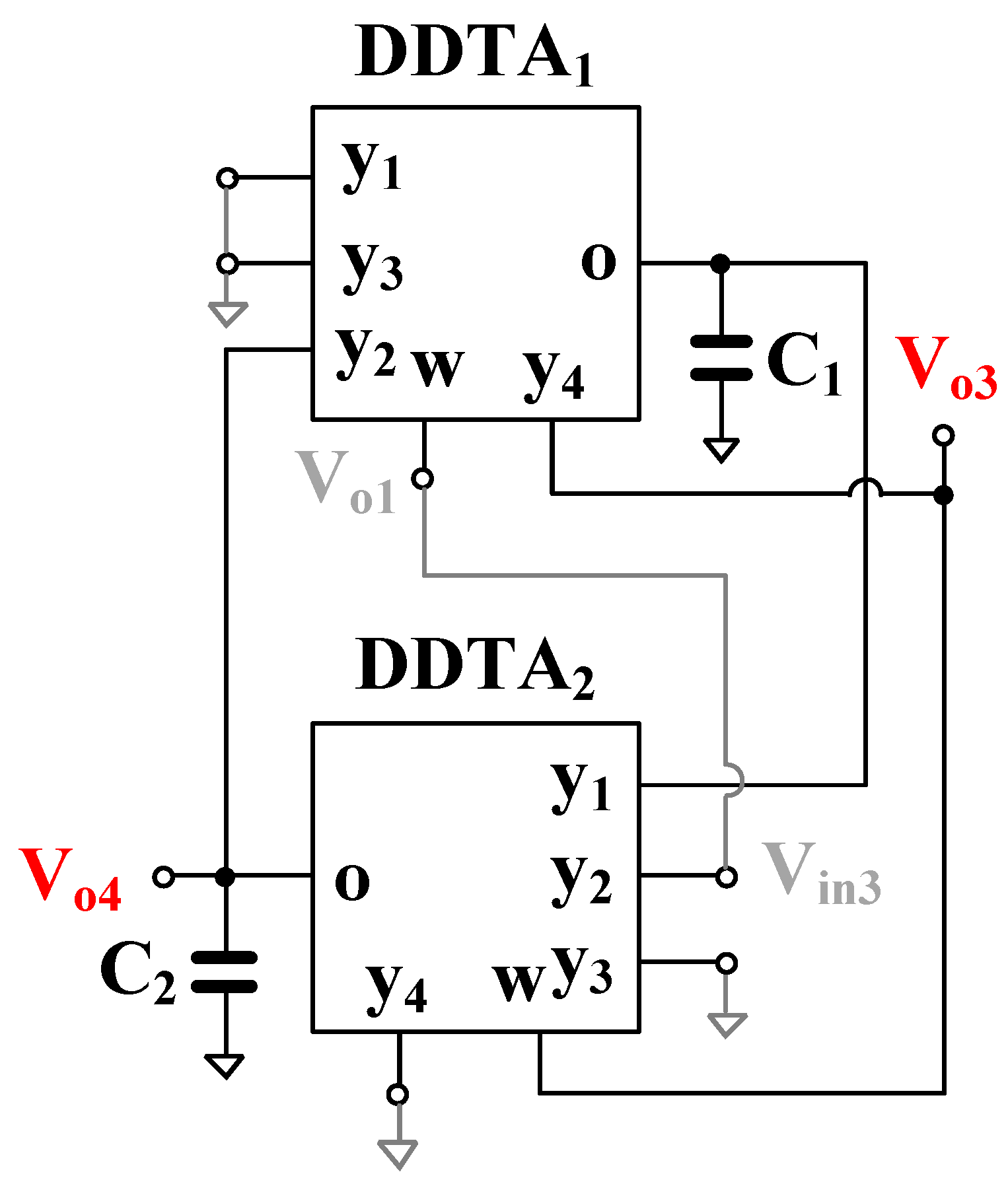
Figure 4 shows the proposed voltage-mode MIMO universal filter. The topology employs two DDTAs and two grounded capacitors. The terminals Vin1, Vin2, Vin3, Vin4, and Vin5 provide high-input impedances, and the terminals Vo1 and Vo3 low-output impedances, whereas the terminals Vo2 and Vo4 require external buffer circuits if a low-impedance load is applied.
From (14)–(17), the low-pass (LP), band-pass (BP), high-pass (HP), band-stop (BS), and all-pass (AP) responses can be obtained by properly applying the input signal and choosing the output terminals as shown in Table 1. The input terminals that are not used should be connected to ground. In the case of the all-pass filtering response, the circuit requires an inverting-type input signal, which can be obtained using additional DDTA.
The natural frequency () and the quality factor () of the filter can be respectively expressed as
From (18) and (19), the natural frequency and the quality factor can be designed, as the quality factor can be given by / by letting = whereas the natural frequency can be obtained electronically by adjusting (= = ).
3.2. Proposed Quadrature Oscillator
The proposed universal filter in Figure 4 was modified to work as a quadrature oscillator as shown in Figure 5. It can be obtained by using a non-inverting BP filtering response and a feedback connection. Using (14), the transfer function between and can be expressed as follows:
Letting = 1, the oscillator characteristic can be derived as
Letting , the condition of oscillation (CO) is
and the frequency of oscillation (FO) is
Thus, the CO of the oscillator can be controlled by and/or , and letting =, the FO can be controlled electronically by (==). Therefore, the FO and CO of the oscillator can be orthogonally controlled. The nodes Vo3 and Vo4 provide quadrature output signals. It can be confirmed by the relationship between Vo3 and Vo4:
Thus, the phase difference between Vo3 and Vo4 is 90°. After setting s = jω0 into (24) and taking into account Equations (22) and (23) and the condition gm1 = gm2, the ratio (24) is one; thus, if oscillation condition (22) is accomplished, the oscillator provides equal amplitudes of both quadrature signals independently of the oscillation frequency.
3.3. Non-Idealities Analysis
Considering non-idealities of the DDTA, (1) can be rewritten as:
where denotes the voltage gain from to of -th DDTA, denotes the voltage gain from to of -th DDTA, and denotes the voltage gain from to of -th DDTA. Ideally, the voltage gains , , and are unity. The is the non-ideal transconductance gain of the DDTA, whose frequency dependence is given by parasitic capacitance Co and resistance Ro at o-terminal. In the frequency range near the cutoff frequency, can be approximated as [48]
where , denotes the first-order pole.
Considering the denominator D(s) of (27)–(30), the modified parameters and can be expressed by:
From (27), the modified oscillator characteristic can be expressed as
The modified CO and FO of the oscillator are then
Since this work is focused on circuits that operate at low frequency, Equation (26) is not taken in consideration. In the case that the universal filter and the quadrature oscillator operate in the frequency range in which the frequency dependence of gm asserts its influence, then (26) should be used to refine the error analysis.
4. Simulation Results
The DDTA circuit and its applications were designed in a Cadence environment, using 130 nm CMOS technology from UMC. The transistor’s aspect ratio and values of passive devices are included in Table 2. The voltage supply is 0.3 V (VDD = −VSS = 0.15 V), the bias current of the DDCC IB = 50 nA, and the nominal value of the setting current of the TA Iset = 500 nA. The nominal power consumption of the DDTA is 357.4 nW (DDCC = 70.21 nW, TA = 287.2 nW). The input and compensation capacitors are highly linear metal–isolator–metal capacitors (MIM). The linear resistor R is a high-resistance poly-resistor.
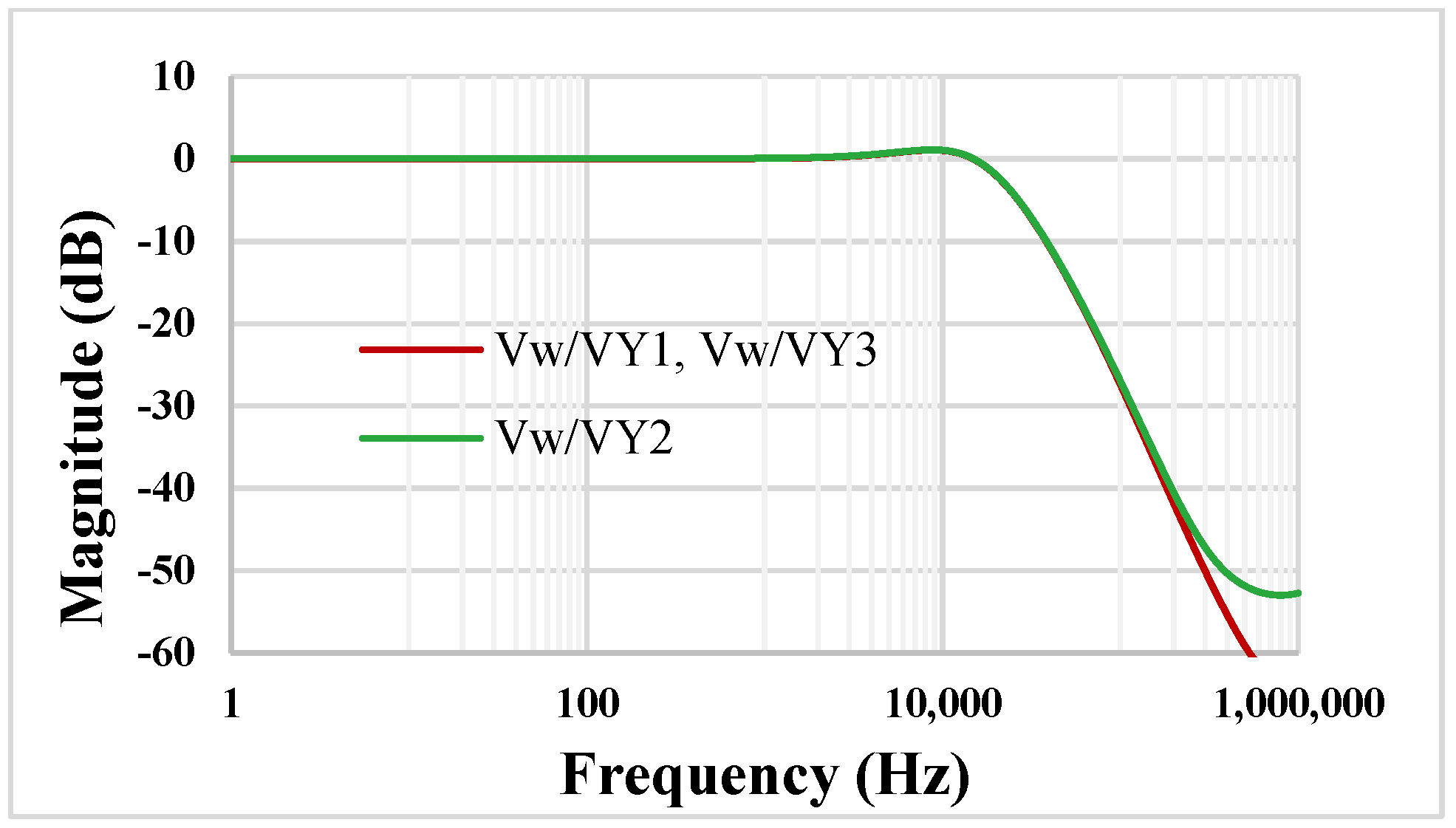
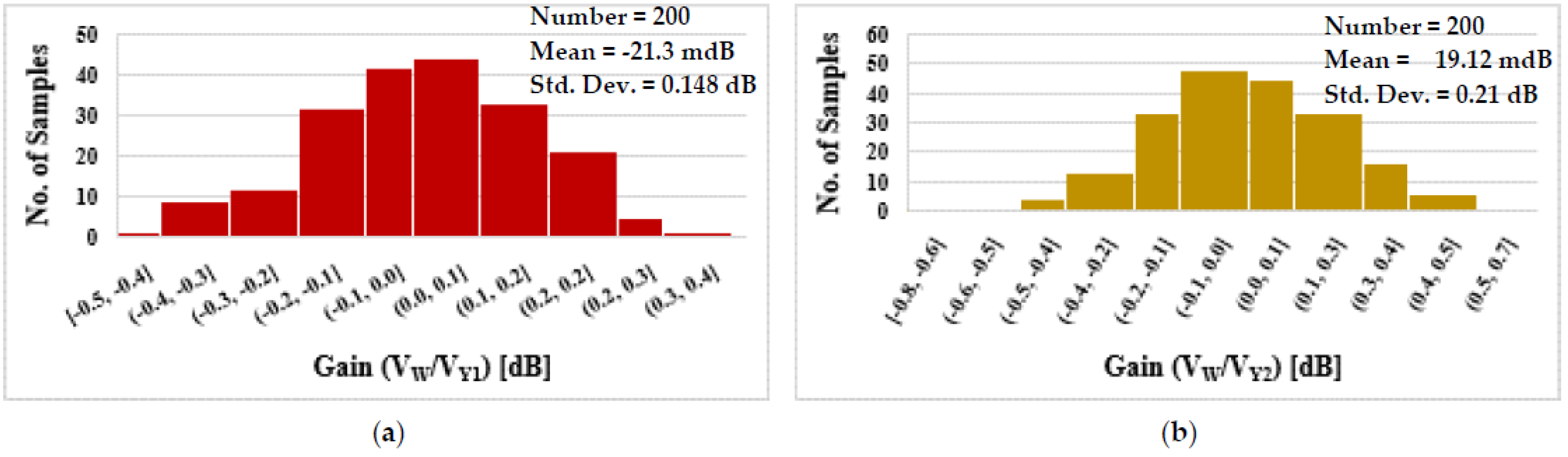
The open-loop gain of the DDCC (i.e., without the unity gain feedback) was simulated as 73.9 dB, and the phase margin was 56.2° for 20 pF load capacitor. The simulated magnitude characteristics of the DDCC are shown in Figure 6. The low-frequency gain for VW/VY1 (=VW/VY3) and VW/VY2 is 14 mdB and 57.29 mdB, while the −3 dB bandwidth is 22.24 kHz and 22.23 kHz, respectively.
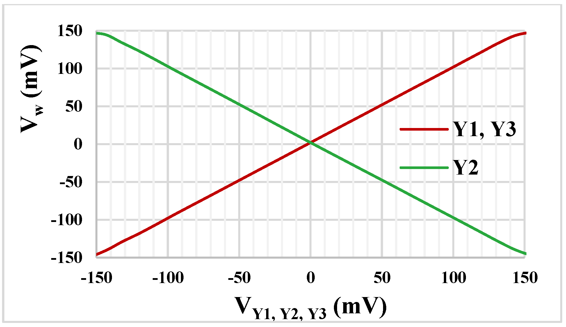
The simulated DC transfer characteristics of the DDCC are shown in Figure 7. As is evident, the DDCC enjoys rail-to-rail operation for all its inverting and non-inverting inputs. This rail-to-rail operation capability is a design achievement.
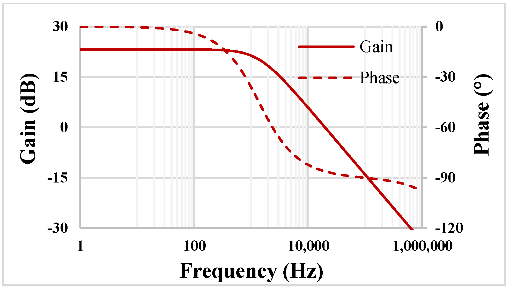
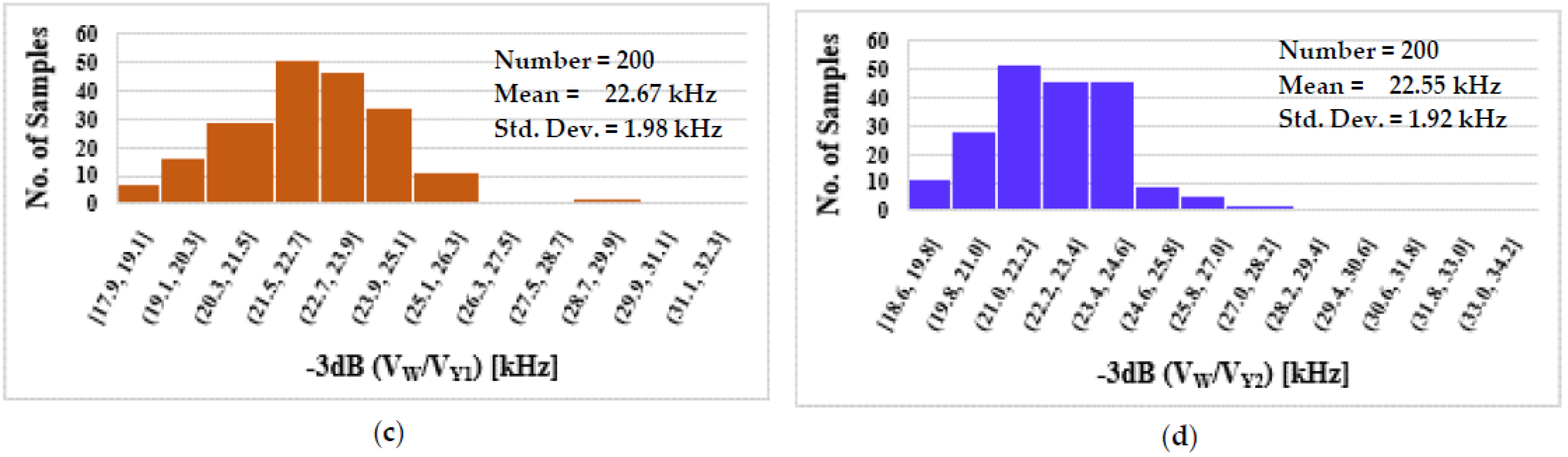
The simulated gain and phase characteristics for the TA with Iset = 0.5 µA and 20 pF load capacitance are shown in Figure 8. The low DC gain is 23.2 dB, and the bandwidth (BW) is 19.65 kHz, while the phase error is 3.8°.
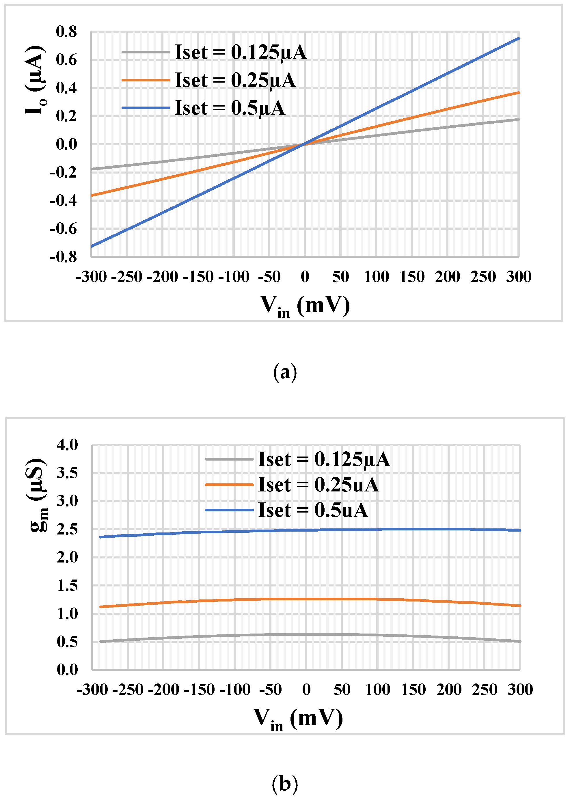
Figure 9a,b shows the DC characteristic of the output current and the transconductance versus fully differential input voltage Vin (Vin = V+ − Vy4) for the TA for Iset = 0.125 µA, 0.25 µA, and 0.5 µA. The rail-to-rail operation with high linearity is evident.
To determine the impact of mismatch and process variation on the circuit’s performance, Monte Carlo (MC) simulations (200 runs) were carried out. As the histograms show in Figure 10, the impact of mismatch and process variation on the gain and −3 dB BW of the DDCC is low. The impact is also low on the gain and phase error of the TA as shown in Figure 11.
The process, voltage, temperature (PVT) corners analysis was also provided on the proposed DDTA. The MOS transistor corners were slow-slow, slow-fast, fast-slow, and fast-fast, the voltage supply corners were (VDD − VSS) ± 10%, and the temperature corners were −20 °C and 70 °C. Table 3 and Table 4 show the results of the minimum, nominal, and maximum values of the gain, −3 dB BW for the DDCC, and gain and phase error for the TA. The impact of the PVT corners in all cases is acceptable.
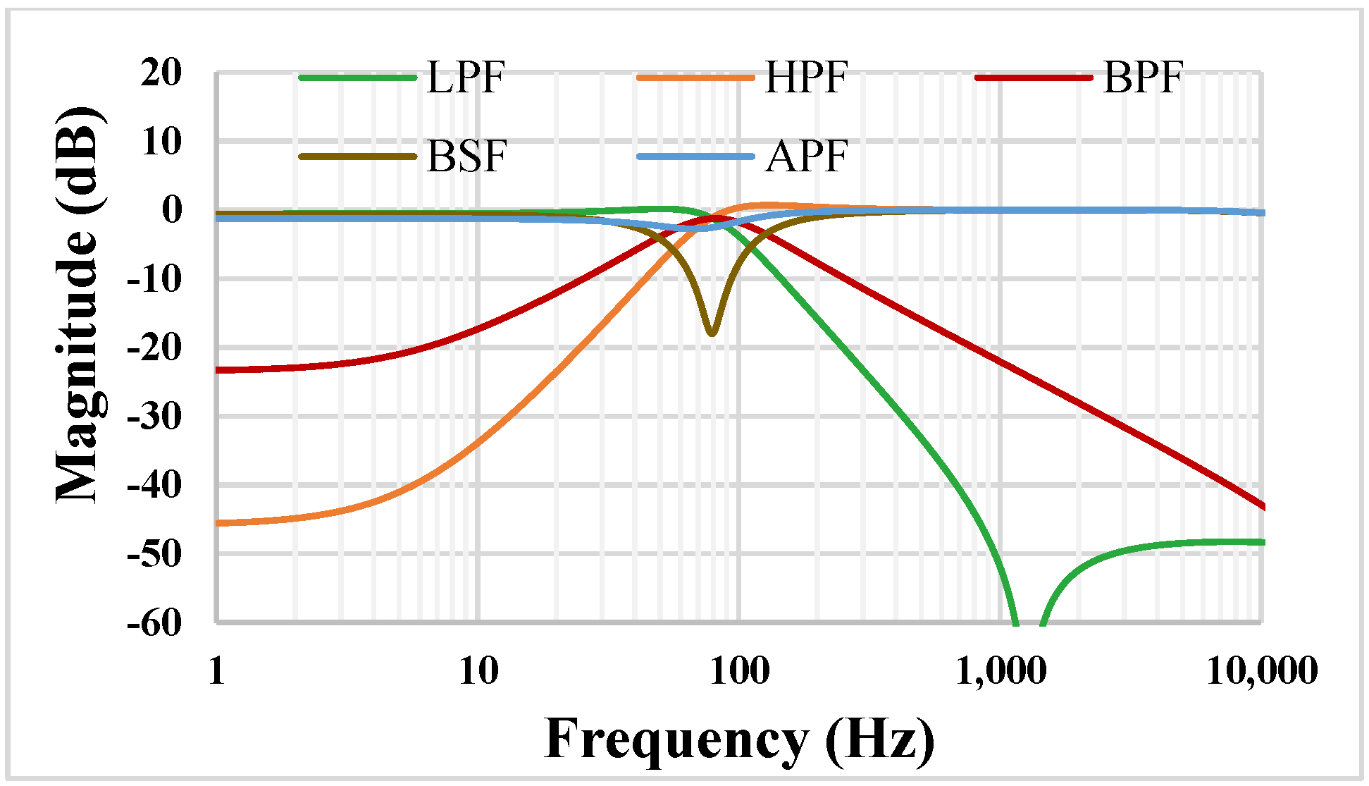
The universal filter in Figure 4 was simulated for C1 = C2 = 5 nF, which are off-chip capacitors. The magnitude characteristics of the LPF, HPF, BPF, BSF, and APF are shown in Figure 12. The simulated natural frequency (fo) is around 81.47 Hz. It is worth mentioning that, due to the limited value of the output resistance of the TA, which is around 5.1 MΩ, the attenuations of the HPF and BPF are degraded at low frequencies. Therefore, if an application demands higher attenuation, then the output resistance could be increased, employing the MOS transistor self-cascode technique.
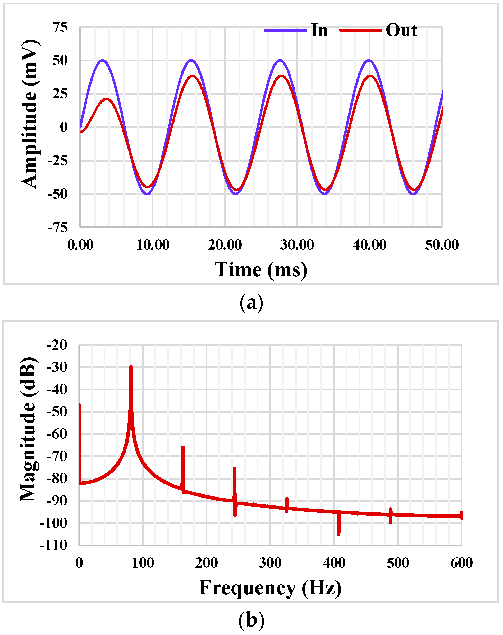
The BPF was tested by applying a sine wave signal Vin = 100 mVpp @ 81.47 Hz. The waveforms of the input and output voltages are shown in Figure 13a. The spectrum of the output signal is shown in Figure 13b, where the total harmonic distortion (THD) of the BPF output is 0.5%.
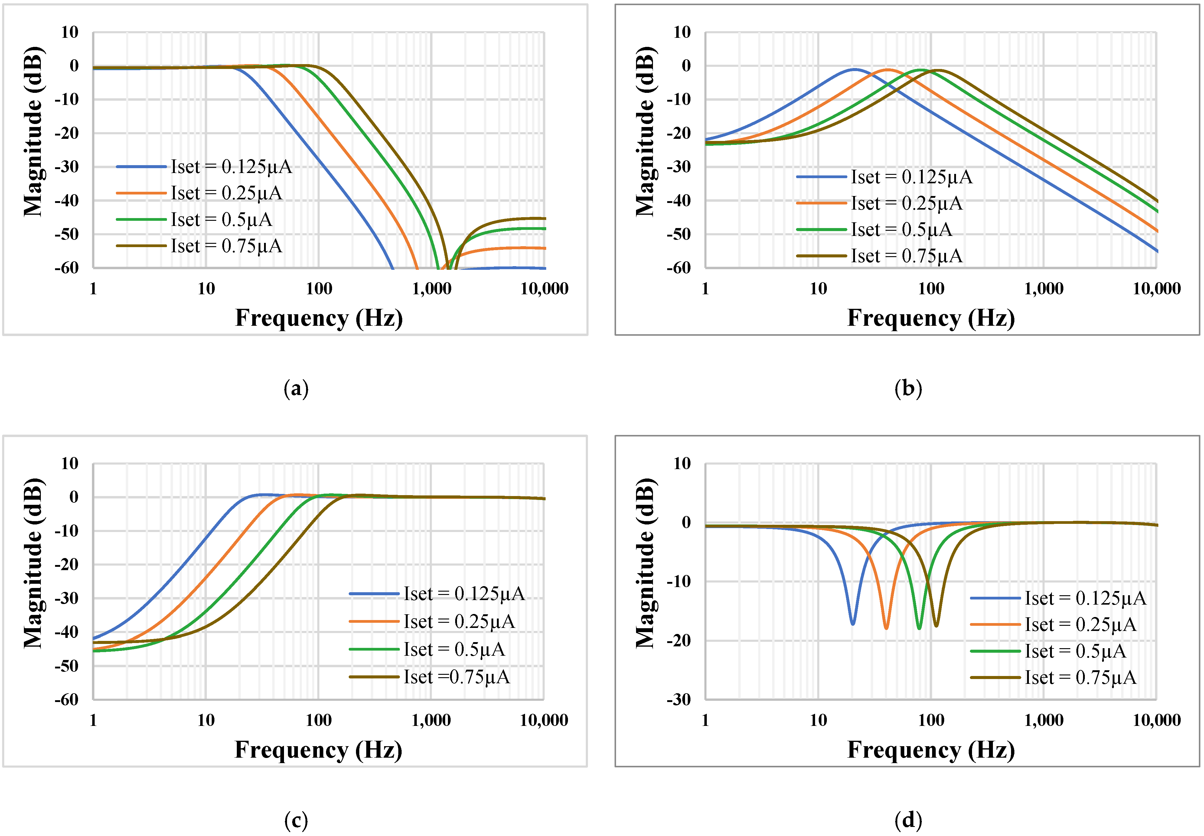
The electronic tuning capability of the LPF, BPF, HPF, and BSF with different bias currents, Iset = 0.125, 0.25, 0.5, and 0.75 µA, is shown in Figure 14. The fo was in the range of 21.11 Hz, 41.63 Hz, 81.47 Hz, and 115.74 Hz, respectively.
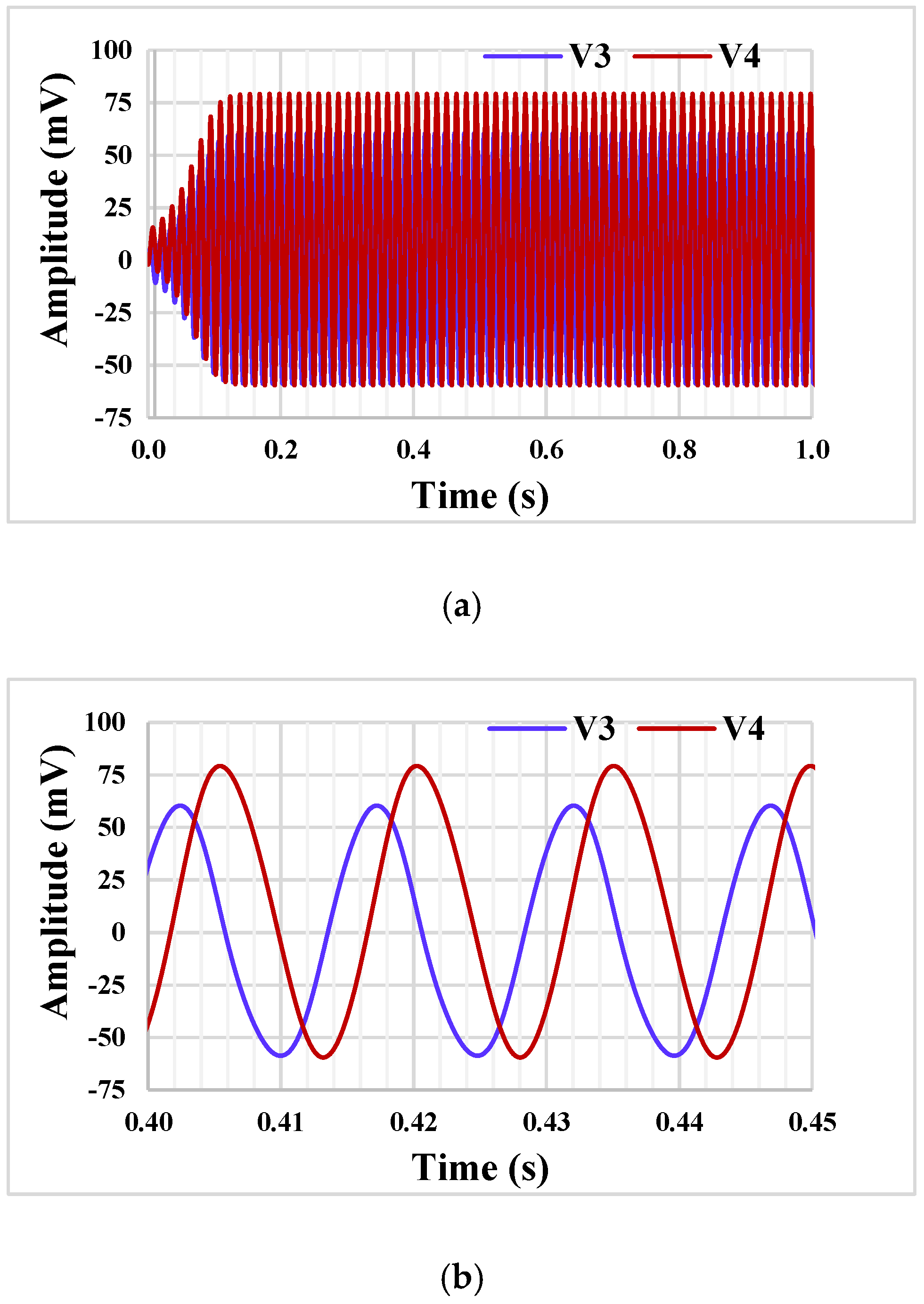
The simulation results showing the start of the oscillation and the steady state of the quadrature oscillator from Figure 5 are given in Figure 15. The oscillation frequency is 67 Hz, and the THD for outputs V3 and V4 are 1.2% and 1.29%, respectively.
Finally, Table 5 provides the comparison of the proposed filter with others in the literature [23,41,42,44,46,47]. It is evident that the proposed filter offers the highest number of filtering functions with lowest power supply and power consumption, thanks to the innovative CMOS structure of the DDTA.
5. Conclusions
This paper presents an innovative structure of a DDTA capable of operating under an extremely low voltage supply of 0.3 V while offering a rail-to-rail input voltage swing. As an application, a universal filter and quadrature oscillator based on two DDTAs and two grounded capacitors are presented. The simulation results including Monte Carlo and PVT analysis confirm the good functionality of the proposed circuits.
Author Contributions
Conceptualization: F.K. and M.K.; Methodology: F.K., M.K., T.K. and D.B.; Validation: F.K., M.K. and T.K.; Formal Analysis: M.K., T.K., F.K. and D.B.; Investigation: F.K. and M.K.; Writing—Original Draft Preparation: F.K., M.K., T.K. and D.B.; Writing—Review and Editing: F.K., M.K., T.K. and D.B. All authors have read and agreed to the published version of the manuscript.
Funding
This work was supported by the School of Engineering, King Mongkut’s Institute of Technology Ladkrabang, under Grant 2565-02-01-005, and by the University of Defence Brno within the Organization Development Project VAROPS.
Conflicts of Interest
The authors declare no conflict of interest.
References
- Kulej, T. 0.5 V bulk driven CMOS operational amplifier. IET Circuits Dev. Syst. 2013, 7, 352–360. [Google Scholar] [CrossRef]
- Kulej, T. 0.4-V bulk-driven operational amplifier with improved input stage. Circuits Syst. Signal Processing 2015, 34, 1167–1185. [Google Scholar] [CrossRef]
- Kulej, T.; Khateb, F. Design and implementation of sub 0.5-V OTAs in 0.18 µm CMOS. Int. J. Circuit Theory Appl. 2018, 46, 1129–1143. [Google Scholar] [CrossRef]
- Kulej, T.; Khateb, F.; Arbet, D.; Stopjakova, V. A 0.3-V high linear rail-to-rail bulk-driven OTA in 0.13 µm CMOS. IEEE Trans. Circuits Syst.—II Express Briefs 2022, 69, 2046–2050. [Google Scholar] [CrossRef]
- Khateb, F.; Kulej, T.; Akbari, M.; Steffan, P. 0.3-V bulk-driven nanopower OTA-C integrator in 0.18 µm CMOS. Circuits Syst. Signal Process 2019, 38, 1333–1341. [Google Scholar] [CrossRef]
- Colletta, G.D.; Ferreira, L.H.C.; Pimenta, T.C. A 0.25-V 22-nS symmetrical bulk-driven OTA for low frequency Gm–C applications in 130-nm digital CMOS process. Analog Integr. Circuits Signal Process 2014, 81, 377–383. [Google Scholar] [CrossRef]
- Cotrim, E.D.; Ferreira, L.H.C. An ultra-low-power CMOS symmetrical OTA for low-frequency Gm-C applications. Analog Integr. Circuits Signal Process 2012, 71, 275–282. [Google Scholar] [CrossRef]
- Carrillo, J.M.; Torelli, G.; Valverde, R.P.; Duque-Carrillo, J.F. 1-V Rail-to-Rail CMOS OpAmp with Improved Bulk-Driven Input Stage. IEEE J. Solid-State Circuits 2007, 42, 508–517. [Google Scholar] [CrossRef]
- Vlassis, S.; Raikos, G. Bulk-driven differential voltage follower. Electron. Lett. 2009, 45, 1276–1277. [Google Scholar] [CrossRef]
- Raikos, G.; Vlassis, S. 0.8 V bulk-driven operational amplifier. Analog Integr. Circ. Signal Process 2010, 63, 425–432. [Google Scholar] [CrossRef]
- Carrillo, J.M.; Torelli, G.; Domínguez, M.A.; Pérez-Aloe, R.; Valverde, J.M.; Duque-Carrillo, J.F. A Family of Low-Voltage Bulk-Driven CMOS Continuous-Time CMFB Circuits. IEEE Trans. Circuits Syst. II 2010, 57, 863–867. [Google Scholar] [CrossRef]
- Raikos, G.; Vlassis, S.; Psychalinos, C. 0.5 V bulk-driven analog building blocks. Int. J. Electron. Commun. (AEÜ) 2012, 66, 920–927. [Google Scholar] [CrossRef]
- Kulej, T.; Khateb, F. 0.4-V bulk-driven differential-difference amplifier. Microelectron. J. 2015, 46, 362–369. [Google Scholar] [CrossRef]
- Khateb, F.; Kulej, T. Design and implementation of a 0.3-V differential difference amplifier. IEEE Trans. Circuits Syst. I Regul. Pap. 2019, 66, 513–523. [Google Scholar] [CrossRef]
- Lopez-Martin, A.J.; Ramirez-Angulo, J.; Carvajal, R.G.; Acosta, L. CMOS Transconductors with Continuous Tuning Using FGMOS Balanced Output Current Scaling. IEEE J. Solid State Circuits 2008, 43, 1313–1323. [Google Scholar] [CrossRef]
- Rico-Aniles, H.D.; Ramirez-Angulo, J.; Lopez-Martin, A.J.; Carvajal, R.G. 360 nW Gate-Driven Ultra-Low Voltage CMOS Linear Transconductor with 1 MHz Bandwidth and Wide Input Range. IEEE Trans. Circuits Syst. II Express Briefs 2020, 67, 2332–2336. [Google Scholar] [CrossRef]
- Khateb, F.; Prommee, P.; Kulej, T. MIOTA-based Filters for Noise and Motion Artifact Reductions in Biosignal Acquisition. IEEE Access 2022, 10, 14325–14338. [Google Scholar] [CrossRef]
- Kumngern, M.; Aupithak, N.; Khateb, F.; Kulej, T. 0.5V Fifth-Order Butterworth Low-Pass Filter Using Multiple-Input OTA for ECG Applications. Sensors 2020, 20, 7343. [Google Scholar] [CrossRef]
- Jaikla, W.; Khateb, F.; Kumngern, M.; Kulej, T.; Ranjan, R.K.; Suwanjan, P. 0.5 V Fully Differential Universal Filter Based on Multiple Input OTAs. IEEE Access 2020, 8, 187832–187839. [Google Scholar] [CrossRef]
- Prommee, P.; Karawanich, K.; Khateb, F.; Kulej, T. Voltage-Mode Elliptic Band-Pass Filter Based on Multiple-Input Transconductor. IEEE Access 2021, 9, 32582–32590. [Google Scholar] [CrossRef]
- Kumngern, M.; Kulej, T.; Stopjakova, V.; Khateb, F. 0.5 V Sixth-order Chebyshev band-pass filter based on multiple-input bulk-driven OTA. AEU-Int. J. Electron. Commun. 2019, 111, 152930. [Google Scholar] [CrossRef]
- Kumngern, M.; Kulej, T.; Khateb, F.; Stopjakova, V.; Ranjan, R.K. Nanopower multiple-input DTMOS OTA and its applications to high-order filters for biomedical systems. AEU-Int. J. Electron. Commun. 2021, 130, 153576. [Google Scholar] [CrossRef]
- Kumngern, M.; Khateb, F.; Kulej, T.; Psychalinos, C. Multiple-Input Universal Filter and Quadrature Oscillator Using Multiple-Input Operational Transconductance Amplifiers. IEEE Access 2021, 9, 56253–56263. [Google Scholar] [CrossRef]
- Khateb, F.; Kulej, T.; Akbari, M.; Kumngern, M. 0.5-V High Linear and Wide Tunable OTA for Biomedical Applications. IEEE Access 2021, 9, 103784–103794. [Google Scholar] [CrossRef]
- Khateb, F.; Kulej, T.; Kumngern, M.; Psychalinos, C. Multiple-input bulk-driven MOS transistor for low-voltage low-frequency applications. Circuits Syst. Signal Processing 2019, 38, 2829–2845. [Google Scholar] [CrossRef]
- Khateb, F.; Kulej, T.; Veldandi, H.; Jaikla, W. Multiple-input bulk-driven quasi-floating-gate MOS transistor for low-voltage low-power integrated circuits. AEU-Int. J. Electron. Commun. 2019, 100, 32–38. [Google Scholar] [CrossRef]
- Khateb, F.; Kulej, T.; Kumngern, M.; Jaikla, W.; Ranjan, R.K. Comparative performance study of multiple-input Bulk-driven and multiple-input Bulk-driven Quasi-floating-gate DDCCs. AEU-Int. J. Electron. Commun. 2019, 108, 19–28. [Google Scholar] [CrossRef]
- Jaikla, W.; Khateb, F.; Kulej, T.; Pitaksuttayaprot, K. Universal Filter Based on Compact CMOS Structure of VDDDA. Sensors 2021, 21, 1683. [Google Scholar] [CrossRef]
- Jaikla, W.; Bunrueangsak, S.; Khateb, F.; Kulej, T.; Suwanjan, P.; Supavarasuwat, P. Inductance Simulators and Their Application to the 4th Order Elliptic Lowpass Ladder Filter Using CMOS VD-DIBAs. Electronics 2021, 10, 684. [Google Scholar] [CrossRef]
- Jaikla, W.; Adhan, S.; Suwanjan, P.; Kumngern, M. Current/voltage controlled quadrature sinusoidal oscillators for phase sensitive detection using commercially available IC. Sensors 2020, 20, 1319. [Google Scholar] [CrossRef] [Green Version]
- Ibrahim, M.A.; Minaei, S.; Kuntman, H.A. A 22.5 MHz current-mode KHN-biquad using deferential voltage current conveyor and grounded passive elements. AEU-Int. J. Electron. Commun. 2005, 59, 311–318. [Google Scholar] [CrossRef]
- Alexander, C.K.; Sadiku, M.K.O. Fundamentals of Electric Circuits, 6th ed.; McGraw-Hill: New York, NY, USA, 2017; pp. 655–661. [Google Scholar]
- Povoa, R.; Arya, R.; Canelas, A.; Passos, F.; Martins, R.; Lourenco, N.; Horta, N. Sub-μW Tow-Thomas based biquad filter with improved gain for biomedical applications. Microelectron. J. 2020, 95, 104675. [Google Scholar] [CrossRef]
- Masuch, J.; Restituto, M.D. Low-power quadrature generators for body area network applications. Int. J. Circuit Theory Appl. 2011, 41, 33–43. [Google Scholar] [CrossRef]
- Hu, H.; Gupta, S.; Schiavenato, M. An 143nW relaxation oscillator for ultra-low power biomedical systems. In Proceedings of the 2016 IEEE SENSORS, Orlando, FL, USA, 30 October–3 November 2016; pp. 1–3. [Google Scholar] [CrossRef]
- Tangsrirat, W.; Channumsin, O. High-Input Impedance Voltage-Mode Multifunction Filter Using a Single DDCCTA and Grounded Passive Elements. Radioengineering 2011, 20, 905–910. [Google Scholar]
- Kumngern, M. DDTA and DDCCTA: New active elements for analog signal processing. In Proceedings of the 2012 IEEE International Conference on Electronics Design, Systems and Applications (ICEDSA), Kuala Lumpur, Malaysia, 5–6 November 2012; pp. 141–145. [Google Scholar]
- Kumngern, M. CMOS differential difference voltage follower transconductance amplifier. In Proceedings of the 2015 IEEE International Circuits and Systems Symposium (ICSyS), Langkawi, Malaysia, 2–4 September 2015; pp. 133–136. [Google Scholar] [CrossRef]
- Yesil, A.; Konal, M.; Kacar, F. Electronically Tunable Quadrature Oscillator Employing Single Differential Difference Transconductance Amplifier. Acta Phys. Pol. A 2017, 132, 843. [Google Scholar] [CrossRef]
- Rana, P.; Ranjan, A. Odd- and even-order electronically controlled wave active filter employing differential difference trans-conductance amplifier (DDTA). Int. J. Electron. 2021, 108, 1623–1651. [Google Scholar] [CrossRef]
- Wang, S.-F.; Chen, H.-P.; Ku, Y.; Yang, C.-M. Independently tunable voltage-mode OTA-C biquadratic filter with five inputs and three outputs and its fully-uncoupled quadrature sinusoidal oscillator application. AEU-Int. J. Electron. Commun. 2019, 110, 152822. [Google Scholar] [CrossRef]
- Wang, S.-F.; Chen, H.-P.; Kuu, Y.; Lee, C.-L. Versatile voltage-mode biquadratic filter and quadrature oscillator using four OTAs and two grounded capacitors. Electronics 2020, 9, 1493. [Google Scholar] [CrossRef]
- Wang, S.-F.; Chen, H.-P.; Ku, Y.; Lin, Y.-C. Versatile tunable voltage-mode biquadratic filter and its application in quadrature oscillator. Sensors 2019, 19, 2349. [Google Scholar] [CrossRef] [Green Version]
- Wang, S.-F.; Chen, H.-P.; Ku, Y.; Zhong, M.-X. Analytical Synthesis of High-Pass, Band-Pass and Low-Pass Biquadratic Filters and its Quadrature Oscillator Application Using Current-Feedback Operational Amplifiers. IEEE Access 2021, 9, 13330–13343. [Google Scholar] [CrossRef]
- Faseehuddin, M.; Herencsar, N.; Albrni, M.A.; Sampe, J. Electronically Tunable Mixed-Mode Universal Filter Employing a Single Active Block and a Minimum Number of Passive Components. Appl. Sci. 2021, 11, 55. [Google Scholar] [CrossRef]
- Faseehuddin, M.; Herencsar, N.; Shireen, S.; Tangsrirat, W.; Ali, S.H.M. Voltage Differencing Buffered Amplifier-Based Novel Truly Mixed-Mode Biquadratic Universal Filter with Versatile Input/Output Features. Appl. Sci. 2022, 12, 1229. [Google Scholar] [CrossRef]
- Namdari, A.; Dolatshahi, M. Design of a low-voltage and low-power, reconfigurable universal OTA-C filter. Analog Integr. Circuits Signal Processing 2022. [Google Scholar] [CrossRef]
- Tsukutani, T.; Higashimura, M.; Takahashi, N.; Sumi, Y.; Fukui, Y. Versatile voltage-mode active-only biquad with lossless and lossy integrator loop. Int. J. Electron. 2001, 88, 1093–1102. [Google Scholar] [CrossRef]
Figure 1.
Symbol of DDTA.

Figure 2.
Proposed CMOS structure of DDTA.

Figure 3.
Bulk-driven MI-MOST: (a) symbol, (b) its realization, and (c) realization of RMOS.

Figure 4.
MIMO universal filter using DDTAs.

Figure 5.
The quadrature oscillator.

Figure 6.
The magnitude characteristics of the DDCC.

Figure 7.
The DC transfer characteristics of the DDCC.

Figure 8.
The gain and phase characteristics of the TA.

Figure 9.
The DC output current (a) and transconductance gm (b) characteristics of the TA versus input voltage.
Figure 9.
The DC output current (a) and transconductance gm (b) characteristics of the TA versus input voltage.

Figure 10.
The DDCC histogram of the gain Vw/VY1 (a), Vw/VY2 (b), and the −3 dB BW Vw/VY1 (c), and Vw/VY2 (d).
Figure 10.
The DDCC histogram of the gain Vw/VY1 (a), Vw/VY2 (b), and the −3 dB BW Vw/VY1 (c), and Vw/VY2 (d).


Figure 11.
The TA histogram of the gain (a) and phase error (b).

Figure 12.
The magnitude characteristics of the universal filter.

Figure 13.
The transient response of the BPF (a) and the spectrum of the output signal (b).

Figure 14.
Magnitude characteristics showing the tuning capability of the LPF (a), BPF (b), HPF (c), and BSF (d) with different bias currents.
Figure 14.
Magnitude characteristics showing the tuning capability of the LPF (a), BPF (b), HPF (c), and BSF (d) with different bias currents.

Figure 15.
Starting the oscillation (a) and the steady state (b).


Table 1.
Obtaining variant filtering functions of the proposed filter.
| Filtering Function | Input | Output | |
|---|---|---|---|
| LP | Non-inverting | ||
| Non-inverting | |||
| Inverting | |||
| Non-inverting | |||
| Non-inverting | |||
| Non-inverting | |||
| Inverting | |||
| BP | Non-inverting | ||
| Inverting | |||
| Non-inverting | |||
| Non-inverting | |||
| Inverting | |||
| Non-inverting | |||
| Non-inverting | |||
| Non-inverting | |||
| Inverting | |||
| Inverting | |||
| HP | Non-inverting | ||
| Inverting | |||
| Non-inverting | |||
| BS | Non-inverting | ||
| AP | Non-inverting | ||
Table 2.
Transistor aspect ratios of the DDTA.
| Device | W/L (µm/µm) |
|---|---|
| M1A, M2A, M1B, M2B | 20/3 |
| M7, M8 | 15/3 |
| M3–M6, MB | 10/3 |
| M9 | 6 × 10/3 |
| M10 | 6 × 20/3 |
| MR | 5/3 |
| MIM capacitor: CB = 0.2 pF, Cc = 4 pF | |
| Poly-resistor R = 90 kΩ | |
Table 3.
The PVT corner analysis results for the DDCC.
| DDCC | min. | nom. | max. |
|---|---|---|---|
| P/V/T | P/V/T | ||
| Gain VW/VY1 [mdB] | −75.3/9.8/−224 | 14 | 29.4/14/14 |
| Gain VW/VY2 [mdB] | −14.1/45.8/−75 | 57 | 101/67.3/57 |
| −3 dB VW/VY1 [kHz] | 20.2/22/21 | 22.24 | 25.2/22.1/23.7 |
| −3 dB VW/VY2 [kHz] | 20.1/22/20.8 | 22.23 | 25/22.7/23.4 |
Table 4.
The PVT corner analysis results for the TA.
| TA | min. | nom. | max. |
|---|---|---|---|
| P/V/T | P/V/T | ||
| Gain [dB] | 23/20.6/21.9 | 23.19 | 23.2/25.2/24 |
| Phase error [°] | 3.7/2.9/3.4 | 3.8 | 3.8/5.1/4.3 |
| Gm [µS] | 2.2/2.2/2.2 | 2.48 | 2.5/2.5/2.4 |
Table 5.
Comparison table with other universal filters.
| Features | Proposed | Ref. [23] | Ref. [41] | Ref. [42] | Ref. [44] | Ref. [46] | Ref. [47] |
|---|---|---|---|---|---|---|---|
| Active and passive elements | 2 DDTA, 2 C | 5 OTA, 2 C | 5 OTA, 2 C | 4 OTA, 2 C | 3 CFOA, 2 C, 4 R | 3 VDBA, 2 C, 1 R (Figure 2) | 8 OTA, 2 C (Figure 3) |
| Realization | CMOS structure (130 nm) | CMOS structure (180 nm) & commercial IC | commercial IC | commercial IC | CMOS structure (180 nm) | CMOS structure (180 nm) | CMOS structure (180 nm) |
| Filter type | MIMO | MISO | MIMO | MIMO | MOMO | MISO | MIMO |
| Number of filtering functions | 22 (VM) | 11 (VM) | 13 (VM) | 9 (VM) | 5 (VM) | 20 (Mixed-mode) | 20 (Mixed-mode) |
| Offer universal filter and oscillator | Yes | Yes | Yes | Yes | Yes | No | No |
| Electronic control of parameter | Yes | Yes | Yes | Yes | No | Yes | Yes |
| Natural frequency (kHz) | 0.08147 | 1 | 217 | 144.7 | 757.88. | 16.631 × 10³ | 5.77 |
| Total harmonic distortion (%) | 0.5@100 mVpp | 1.67@600 mVpp | 1.93@200 mVpp | 3.83@170 mVpp | [email protected] Vpp | <3@500 mVpp | <2@200 mVpp |
| Power supply voltages (V) | 0.3 | 1.2 | ±15 | ±15 | ±0.9 | ±1.25 | ±0.3 |
| Simulated power consumption (µW) | 0.715 | 96 | 860 × 103 | 0.92 × 10⁶ | 5.4 × 10³ | 5.482 × 10³ | 5.77 |
| Verification of result | Sim | Sim/Exp | Sim/Exp | Sim/Exp | Sim/Exp | Sim/Exp | Sim |
Note: VDBA = voltage differencing buffered amplifier, VM = voltage-mode.
Publisher’s Note: MDPI stays neutral with regard to jurisdictional claims in published maps and institutional affiliations. |
© 2022 by the authors. Licensee MDPI, Basel, Switzerland. This article is an open access article distributed under the terms and conditions of the Creative Commons Attribution (CC BY) license (https://creativecommons.org/licenses/by/4.0/).
Share and Cite
MDPI and ACS Style
Khateb, F.; Kumngern, M.; Kulej, T.; Biolek, D. 0.3-Volt Rail-to-Rail DDTA and Its Application in a Universal Filter and Quadrature Oscillator. Sensors 2022, 22, 2655. https://doi.org/10.3390/s22072655
AMA Style
Khateb F, Kumngern M, Kulej T, Biolek D. 0.3-Volt Rail-to-Rail DDTA and Its Application in a Universal Filter and Quadrature Oscillator. Sensors. 2022; 22(7):2655. https://doi.org/10.3390/s22072655
Chicago/Turabian StyleKhateb, Fabian, Montree Kumngern, Tomasz Kulej, and Dalibor Biolek. 2022. "0.3-Volt Rail-to-Rail DDTA and Its Application in a Universal Filter and Quadrature Oscillator" Sensors 22, no. 7: 2655. https://doi.org/10.3390/s22072655
Note that from the first issue of 2016, this journal uses article numbers instead of page numbers. See further details here.