1. Introduction
Because of the inherent gain, using linear-mode avalanche photodiodes (APDs) instead of standard pin photodiodes has become attractive in many optical systems where weak optical signal detection is required [
1,
2,
3,
4,
5,
6,
7]. The use of a CMOS process for the production of integrated APDs with electronic circuitry for read-out and signal processing reduces the influence of parasitic effects, and furthermore offers a cost-effective production. Common design approaches towards CMOS-integrated APDs are based on planar n
+/p-well and p
+/n-well junctions. Refs. [
8,
9,
10,
11,
12,
13,
14,
15] present APDs with a thin combined absorption and multiplication region in the order of hundreds of nanometers thickness. These APDs provide a high bandwidth but suffer from low responsivity at long wavelengths (red and near-infrared light) due to their thin detection zone. Refs. [
14,
15] reported APDs that achieve a bandwidth of 8.4 GHz and 12 GHz while their maximum responsivities are 0.56 A/W and 0.03 A/W, respectively, at a wavelength of 850 nm.
In order to achieve a higher responsivity, the so-called reach-through APD was presented, which possesses a separate space-charge region with a larger thickness [
16,
17,
18,
19,
20]. A 12 μm thick absorption region was present in [
17,
19,
20]. In these APDs, the photo-generated electrons in the thick absorption zone drift upwards to the multiplication zone and can trigger the avalanche process, resulting in a high responsivity. However, carrier drift time in their thick absorption region generally limits the bandwidth. Based on the reach-through concept, Ref. [
17] presented an APD with the responsivity and bandwidth of 20.5 A/W and 850 MHz at 670 nm. Refs. [
19,
20] used the lateral well modulation-doping technique to improve the bandwidth by manipulating the electric field distribution within the structure.
One of the main drawbacks of the planar structures is that the photo-sensitive area is proportional to the area of the p/n junction. In fact, since the electric field is limited to below the p/n region, only the carriers generated in this area have a chance to cause impact ionization by electrons drifting to the multiplication region. Therefore, to increase the sensitive area, the p/n junction area has to be expanded, which leads to an increase in the junction’s capacitance. Consequently, these APDs typically exhibit the trade-off between detector capacitance and the detection area. In addition, the proportionality of the active area to the p/n junction area results in a limited fill-factor defined as the ratio of the photo-sensitive area to the whole diode area. Moreover, the necessity of a guard ring to avoid premature edge breakdown in such structures causes further fill-factor degradation. This degradation is more noticeable in the scaled-down APD, where the dimensions of the guard ring are comparable to the photos-sensitive area dimensions. Accordingly, the scalability of such APDs to be used in multi-pixel detectors is an issue [
21,
22,
23].
Guiding carriers generated in the peripheral volume towards the multiplication region can provide a near-unity fill-factor and overcome the scalability issue. A current-assisted avalanche photodiode is presented in [
24] consisting of two electrodes at the surface with different potentials to collect photo-generated carriers in the peripheral volume. This APD achieved a near-unity fill-factor and a responsivity of 13 A/W, but its maximum bandwidth reported was 275 MHz at
λ = 830 nm. Ref. [
25] used the field-line crowding concept with a small n
+/n-well structure to form a distributed electric field over the whole diode volume to guide the photo-generated carriers in the peripheral volume. This device was realized in 0.18 µm CMOS with a 24 µm thick low-doped epitaxial layer. A maximum bandwidth of 1.6 GHz and a responsivity of R = 32 A/W at
λ = 675 nm were achieved for an APD with a radius of 19 μm while having a near-unity fill factor.
This paper presents a dot avalanche-based APD that provides a near-unity fill factor and 9.7 A/W responsivity while achieving 1.8 GHz bandwidth at λ = 675 nm. The single dot structure possesses a small hemispherical n+/p-well structure at the center. A spherically uniform high electric field is formed around the n+/p-well junction, which serves as the multiplication region inside the p-well, and a weaker electric field extends radially throughout the diode to guide charge carriers from the entire diode volume towards the multiplication region. For applications that require a larger light-sensitive area, a multi-dot structure is proposed to increase the active area, which is a combination of several cathode/p-well dots with connected cathodes and with a shared anode. In the next sections, the design approach will be discussed in detail.
2. Single-Dot APD
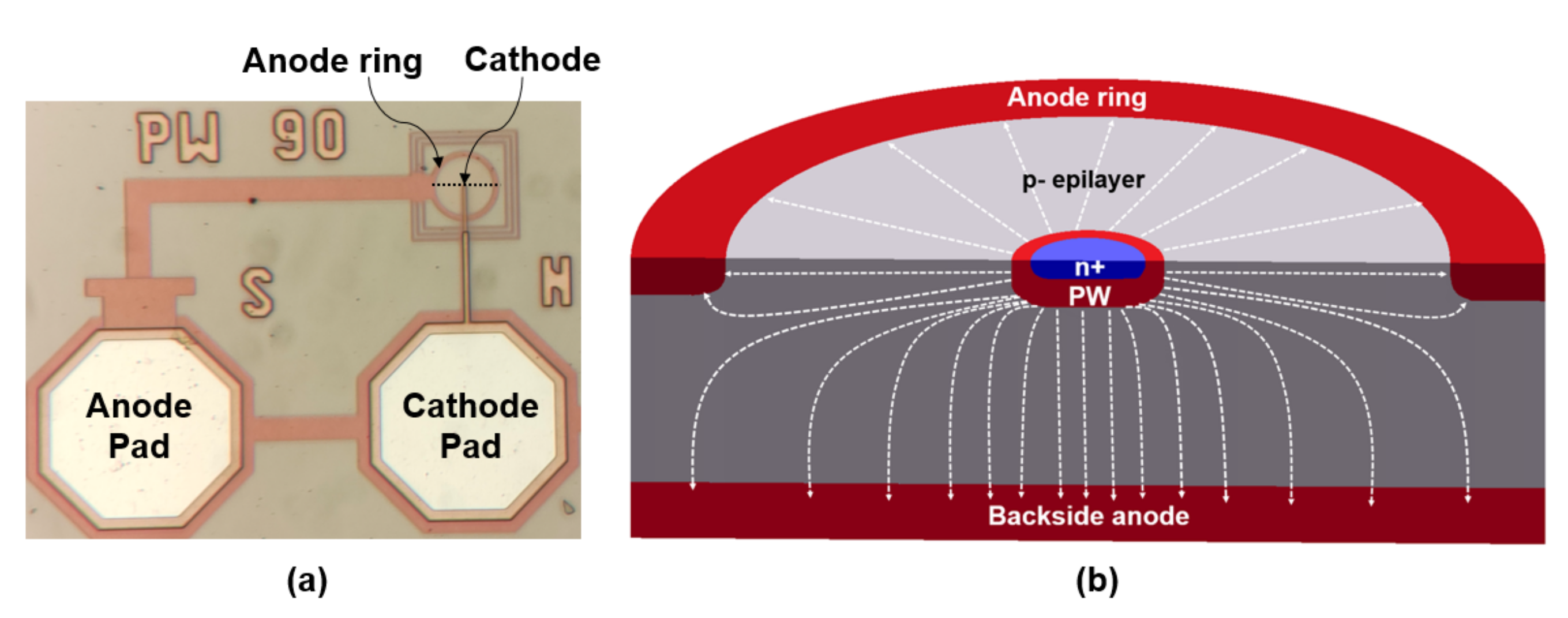
Figure 1 shows the top view (a) and a cross-section (b) of the single-dot APD (SD-APD) fabricated in the 0.35 μm CMOS modular optical sensor technology platform (XO035) of X-FAB semiconductor foundries. A semi-hemispherical high-doped n
+ region embedded in a half-sphere p-well (PW) region as the multiplication region forms the cathode of this APD. The cathode is circularly surrounded by a p
+ and p-well as an anode, which all are formed on a lightly p-doped epitaxial layer (p- epi) with a doping concentration of ∼
cm
and a thickness of ∼12 μm. The p
+ substrate is also used as a backside anode as it is available at the back side of the chip (because the wafers were thinned by mechanical grinding) and can be connected to the anode supply.
In the SD-APD, unlike the planar structures that only have a vertical electric field, the electric field extends radially throughout the diode, which is used for vertical and peripheral charge collection. TCAD simulation is performed to study the electric field distribution inside the structure. According to the cylindrically symmetric geometry of the structure, two-dimensional (2d) simulations of half of the diode are carried out along one radius in the cylindrical coordinate system. In order to enhance the simulation accuracy and to optimize the simulation time, the mesh of grid points in the cathode region (n+/p-well junction) is refined, while it becomes coarser towards the substrate and anode ring.
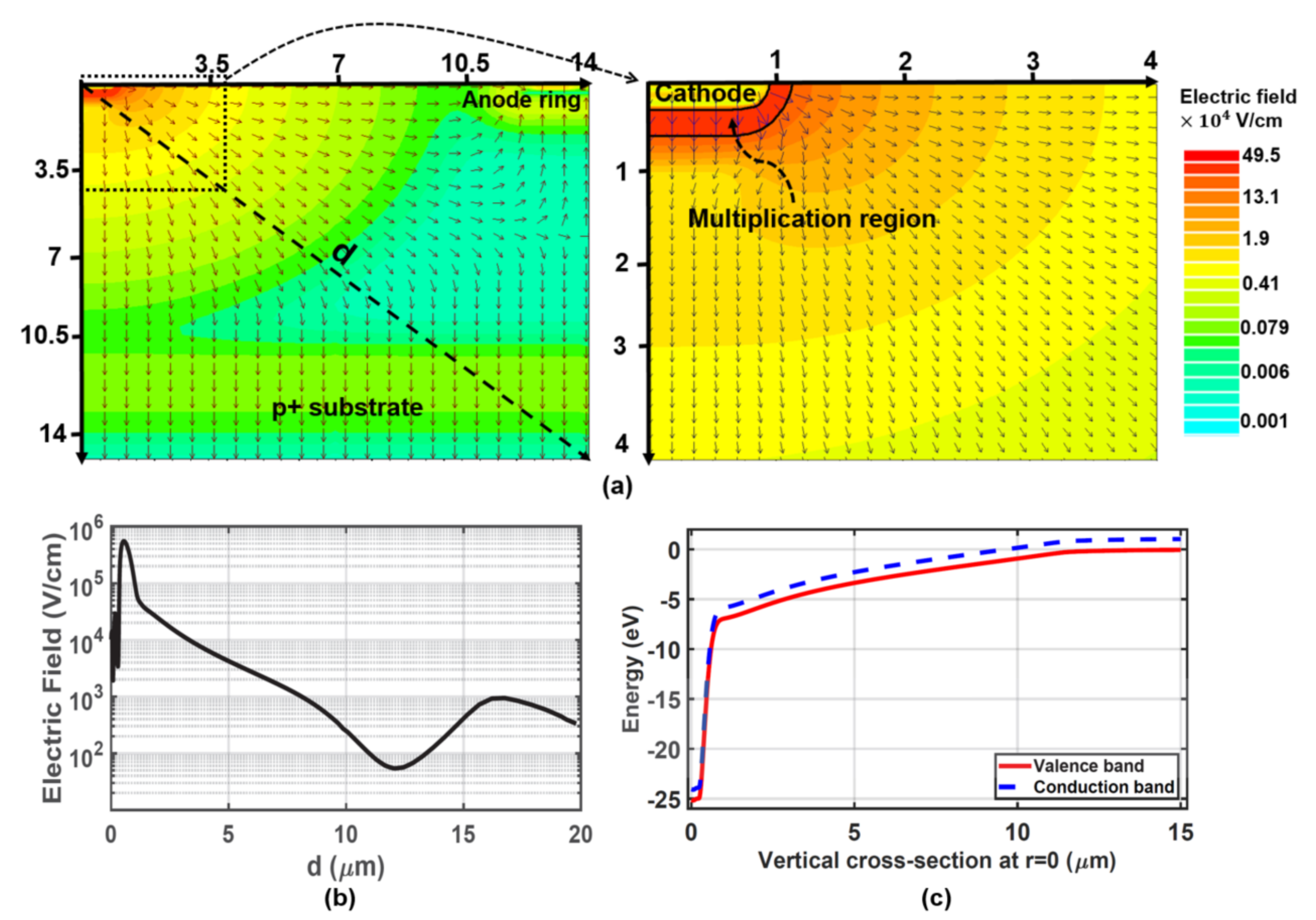
Figure 2a shows a 2d plot of the electric field in the SD-APD at an operating voltage of 24.5 V (breakdown voltage = 25.2 V) simulated using the SILVACO Atlas. It can be seen that a semi-hemispherical multiplication region with a high electric field strength of 4.95 × 10
5 V/cm is formed at the junction of n
+/p-well with a width of ∼0.4 μm at the critical field strength for impact ionization of 2 × 10
5 V/cm. Based on TCAD simulation results and according to the design rules and doping profiles associated with the 0.35 μm XO035 CMOS technology, the n
+ and p-well radii were set to 0.85 μm and 0.9 μm, respectively, to achieve a uniform high-field hemispherical distribution. It should be noted that the 0.85 μm size for the n+ region radius is the minimum size available to form a round n
+ region based on the design rules and doping profiles of the 0.35 μm XO035 CMOS technology. Simulation results indicate that a p-well radius of less than 0.9 μm results in a non-uniform electric field distribution.
The electric field extends but lowers by moving radially away from the cathode towards the substrate, towards the anode ring and in a “diagonal” direction, as shown in
Figure 2b. For example, at a “diagonal” distance of d = 10 μm from the origin of coordinates, the electric field is still ∼200 V/cm.
Figure 2c shows the energy band diagram along a vertical cross-section at r = 0 μm. According to the energy band diagram when a photon is absorbed in the detection region, the generated electron and the hole are promptly separated by the electric field (drifting in opposite directions), and then, the electron drifts into the direction opposite to the electric field vector arrows towards the small multiplication region. This figure also shows that the reverse voltage of 24.5 V splits into about 7.5 V over the thick absorption region and 17 V over the multiplication region. In fact, due to the existence of the lateral component of the electric field, the peripheral carriers also have a chance to reach the multiplication region, where they can start impact ionization. Therefore, the whole diode area acts as the detection zone, which results in a large light-sensitive area. In addition, the drift-based carrier transport mechanism enhances the detector’s speed performance.
Furthermore, since the electric field penetrates deeply into the structure (e.g., the electric field in a depth of 10 μm at r = 0 is ∼400 V/cm), the detection zone extends down to the p
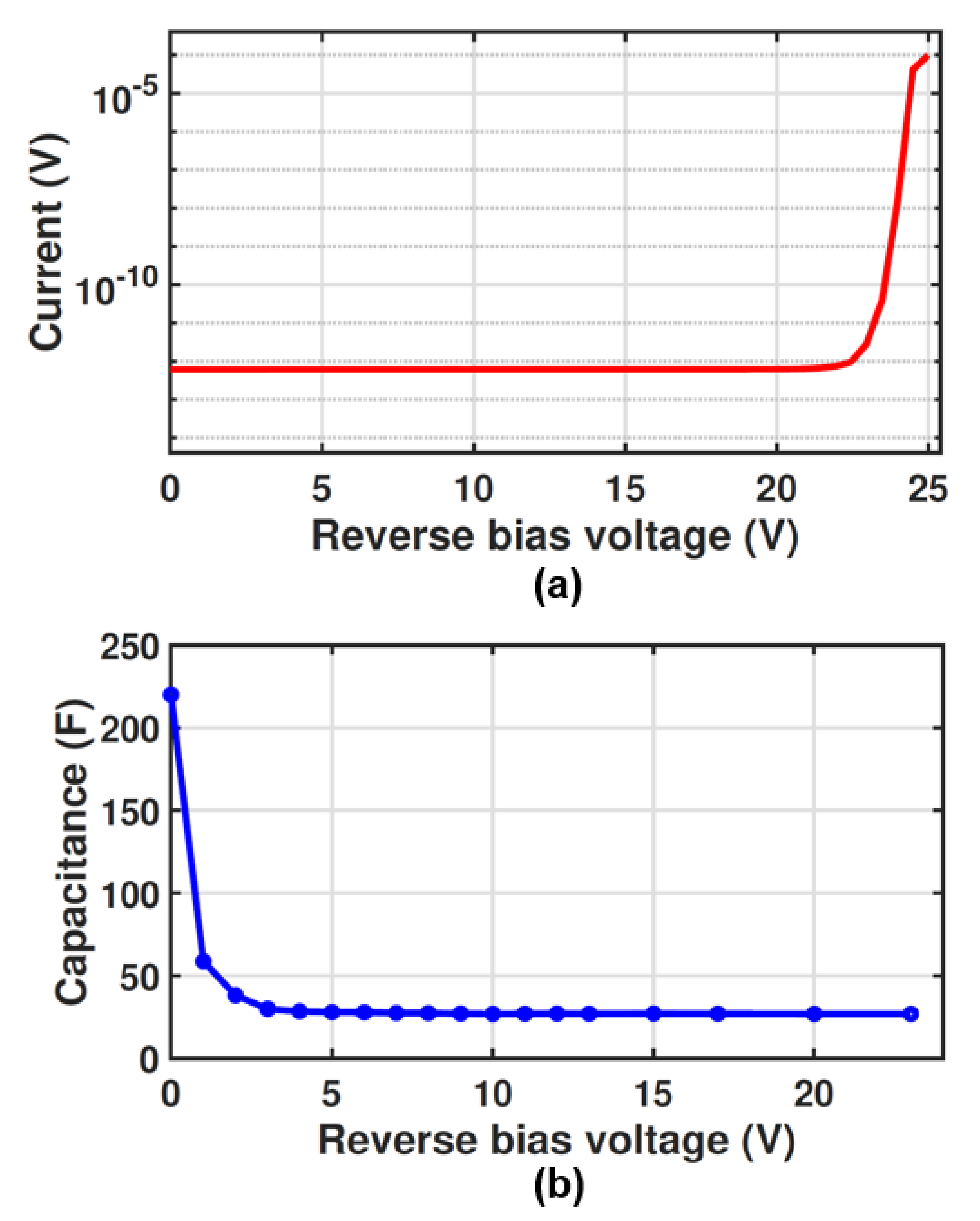
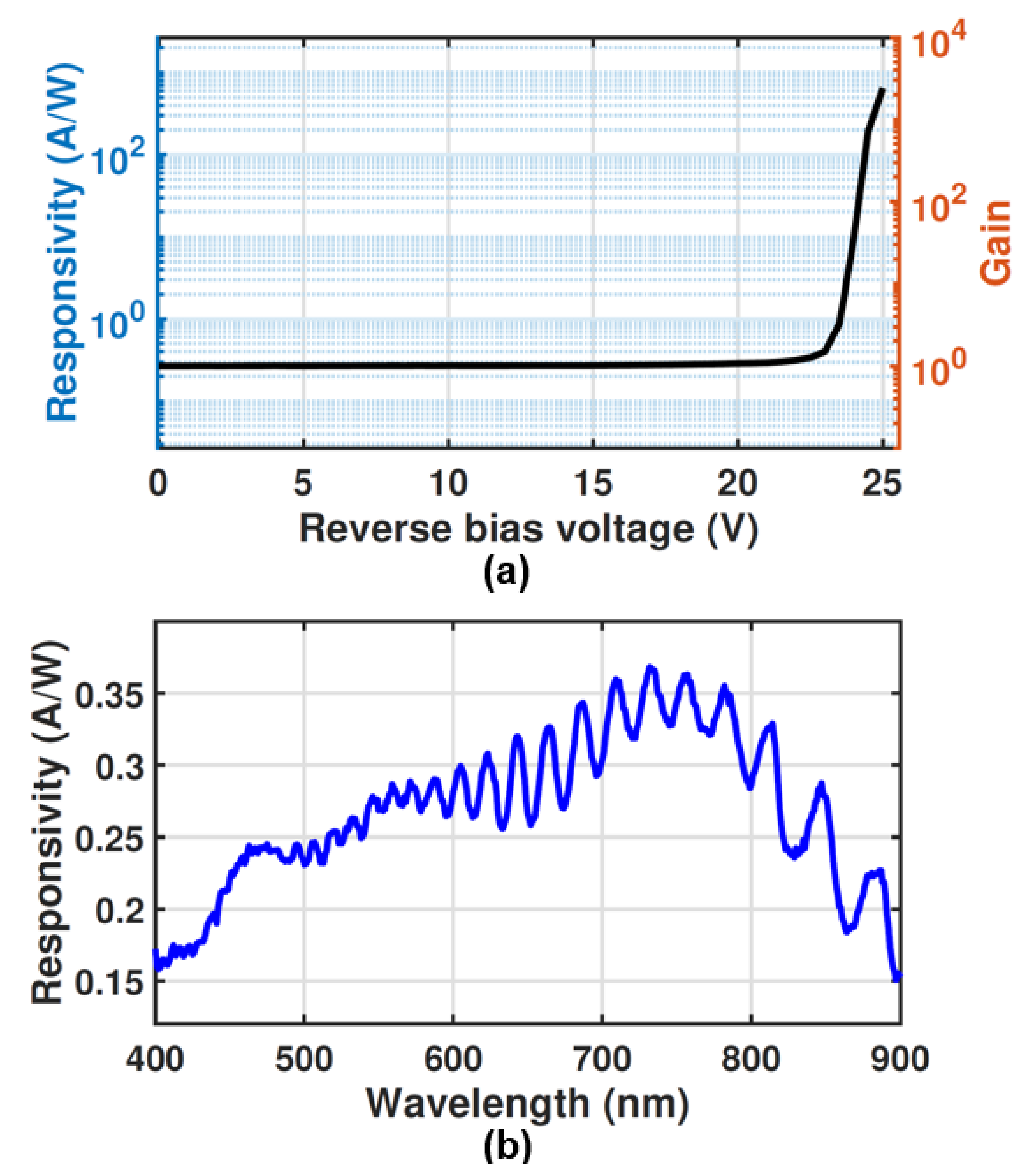
+ substrate, which means the photo-generated carriers in the deep depth can drift towards the multiplication region and trigger an avalanche event. As a result, the large thickness of the detection region provides a high responsivity for long wavelengths. The responsivity and frequency response are assessed through TCAD simulations. The responsivity and bandwidth of 0.27 A/W and 1.25 GHz, respectively, have been obtained for the SD-APD. Such a concentrating electric field distribution causes a breakdown voltage of 25.2 V where the dark current reaches 1 μA [
26] as can be seen in
Figure 3a. However, the breakdown voltage varies as the radius of the p-well changes because the electric field distribution within the structure changes.
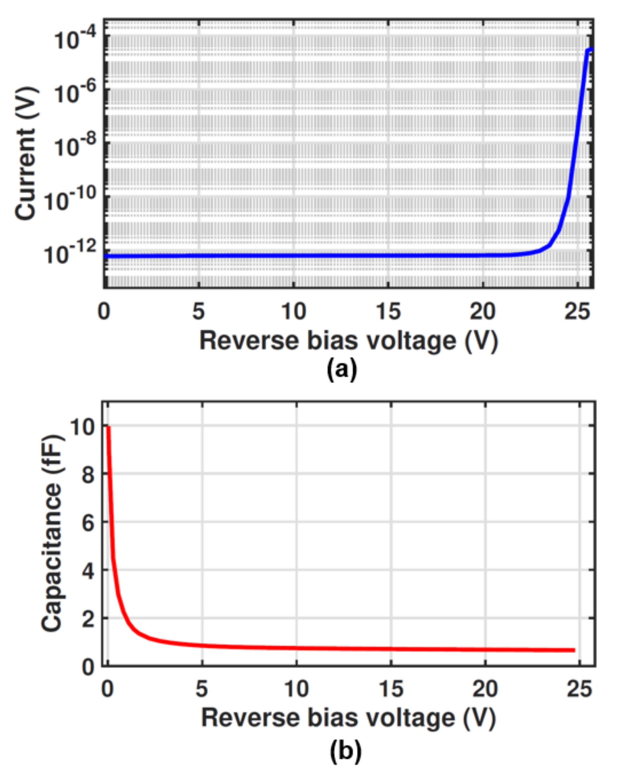
It is worth mentioning that the capacitance of the SD-APD is expected to be low due to the small area of the p/n junction. The capacitance of the SD-APD is evaluated using TCAD simulations as we cannot measure it due to the accuracy of our current equipment.
Figure 3b presents the simulated capacitance of the SD-APD as a function of the reverse bias voltage. It can be seen that the capacitance is ∼10 fF at 0 V bias voltage and quickly drops to sub-Femto Farad values when increasing the reverse bias voltage. At the operating voltage of 24.5 V, the capacitance is 0.65 fF, which is significantly smaller than the typical values of a conventional planar CMOS APDs [
17,
27].
It is important to note that it is not possible to increase the size of the active area only by simply increasing the radius of the surface anode of the diode when a large active area is required (e.g., free space optical communications). Because, as previously shown (
Figure 2), the electric field gradually decreases by moving radially away from the center, and therefore, at distances far from the center, the electric field is very weak or non-existent to drive carriers towards the cathode. Accordingly, the transfer mechanism is no longer carrier drift but carrier diffusion which decreases the responsivity and the bandwidth of the APD. The diffusion transport mechanism leads to a significant reduction in the bandwidth of the APD as the transit time of the photogenerated carriers to reach the cathode strongly increases. However, to increase the active area, a multi-dot structure is proposed, which can provide high responsivity and bandwidth, as detailed below.
3. Multi-Dot APD
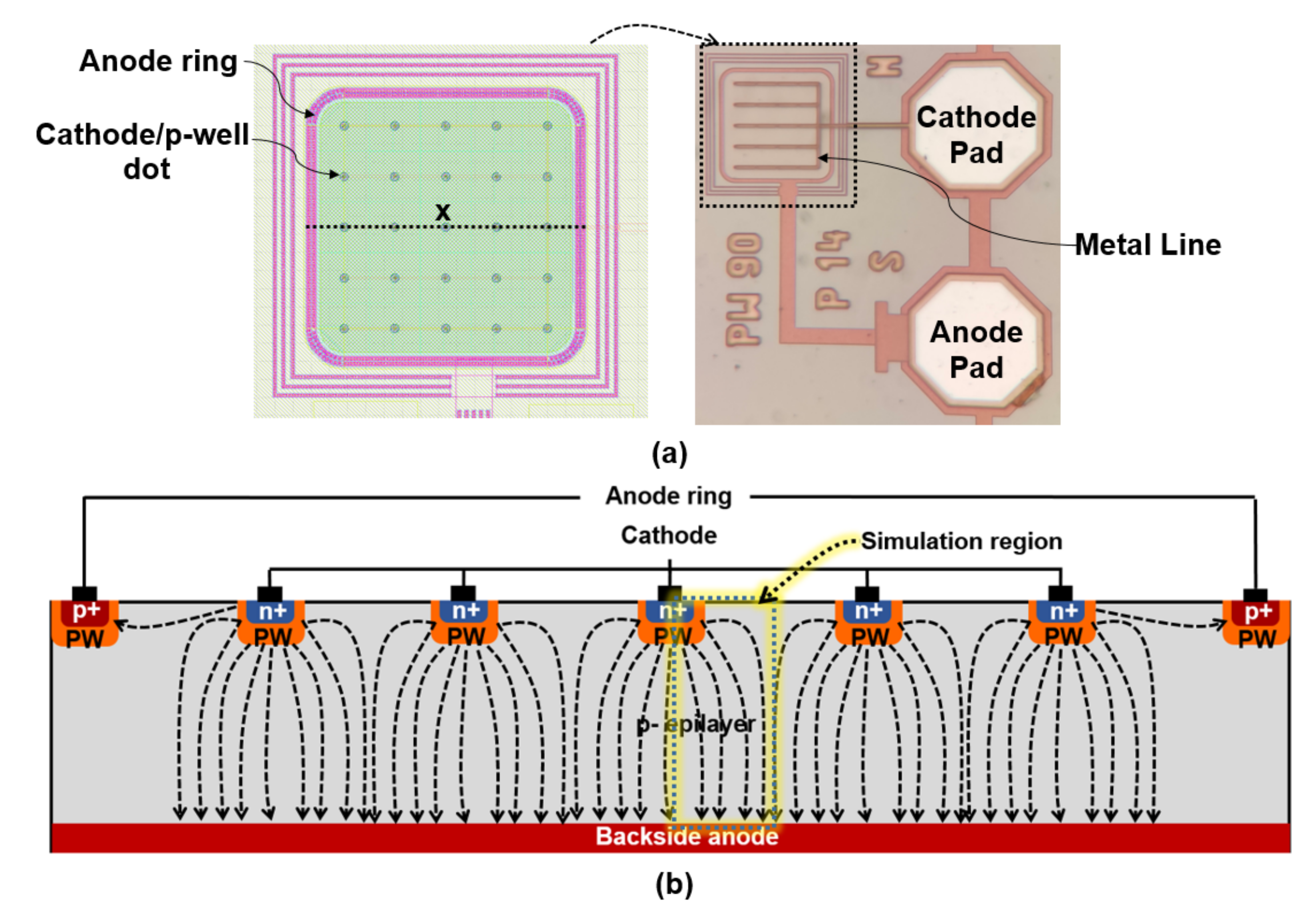
Figure 4 shows the top view (a) and a 2d schematic cross-section (b) of the multi-dot APD (MD-APD) fabricated in the XO035 CMOS technology. The MD-APD is an array (5 × 5) of single-dot cathode/p-well structures, where the single cathodes are connected with tracks in metal layer 4 with a minimum width of 0.6 μm as shown in
Figure 4a. The p
+ substrate is used as a shared backside anode. In addition, the dot cathode array is surrounded by a surface anode where the electric field of the boundary dots terminates, and defines the size of the diode. The APD is covered by the standard isolation and passivation stack to protect the fabricated device from environmental influences.
When the MD-APD is reversely biased, the hemispherical multiplication region is formed around each cathode dot. The area between the dots is fully depleted. The longest electric-field lines with the weakest electric field strength (between two dots) are high-lighted in
Figure 4b. Therefore, the region under and between each cathode acts as a detection zone so that the photo-generated carriers are accelerated towards a cathode according to the local electric field direction. As a result, this structure achieves a large active area, while having a high responsivity and bandwidth.
Based on this approach, the active area can be easily enlarged by expanding the cathode dot array. In fact, the active area can be enlarged by increasing the number of cathode dots arrays and also by increasing the distance between the cathode dots (i.e., the array’s pitch size). However, the pitch size of the array is an important parameter that affects the performance.
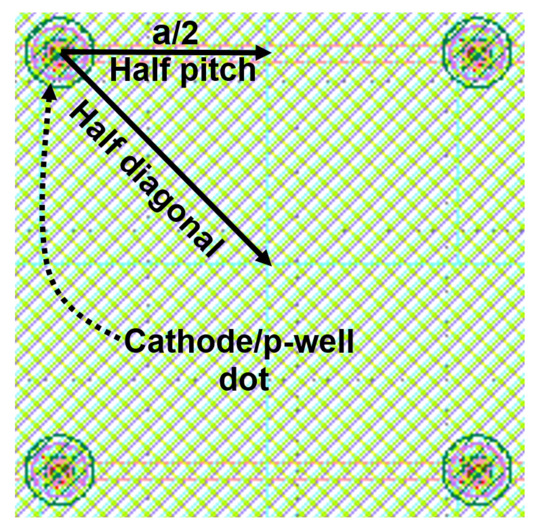
Figure 5 is a zoomed top view of a cathode/p-well dot adjacent to other cathode/p-well dots in the array to visualize a half pitch and a half diagonal from the cathode center. The slowest response is expected if a photon is absorbed exactly in the center between four cathode/p-well dots, because this is where the longest drift distance along the silicon surface appears. This maximum lateral drift distance is
, where
a is the pitch of the n
+/p-well dot array.
If the cathode dots are too far apart, there may not be a large enough electric field in the entire area between two cathodes to drive the photo-generated carriers to the cathode spot. Because, as discussed earlier, the electric field gradually drops by moving away from the center (multiplication region). Therefore, one cannot say that the entire area between two cathode/p-well dots is the detection zone, if the dots are too far apart. In addition, increasing the array’s pitch size results in a lower bandwidth. This is due to the fact that the frequency response is determined by the transit time of photogenerated electrons to reach the cathode. The transit time depends on the carrier drift distance as well as the drift velocity, which is proportional to the local electric field strength. Accordingly, the transit time is expected to be higher in MD-APD with a larger array pitch size because the carrier drift distance increases and, additionally, the intensity of the electric field decreases over the larger distance from the cathode dots.
On the other side, in the case where the distance between two neighboring cathodes is small, more cathode dots are required to achieve the same active area compared to that of the MD-APD with larger pitch sizes. Increasing the number of cathode dots leads to an increase in the MD-APDs capacitance due to the fact that the MD-APDs capacitance is the sum of the capacitance of all single dots in the array plus parasitic capacitance (of metal tracks). In addition, in the MD-APDs with small pitch sizes, more metal lines are needed to connect the cathodes together, leading to a larger parasitic capacitance. Furthermore, a larger area of the detection zone is covered by metal, which is an opaque material. Therefore this area is practically no longer called an absorption region because the incident photons are reflected by the metal before reaching the silicon. Accordingly, the pitch size of the array need to be optimized based on the requirements of the intended application.
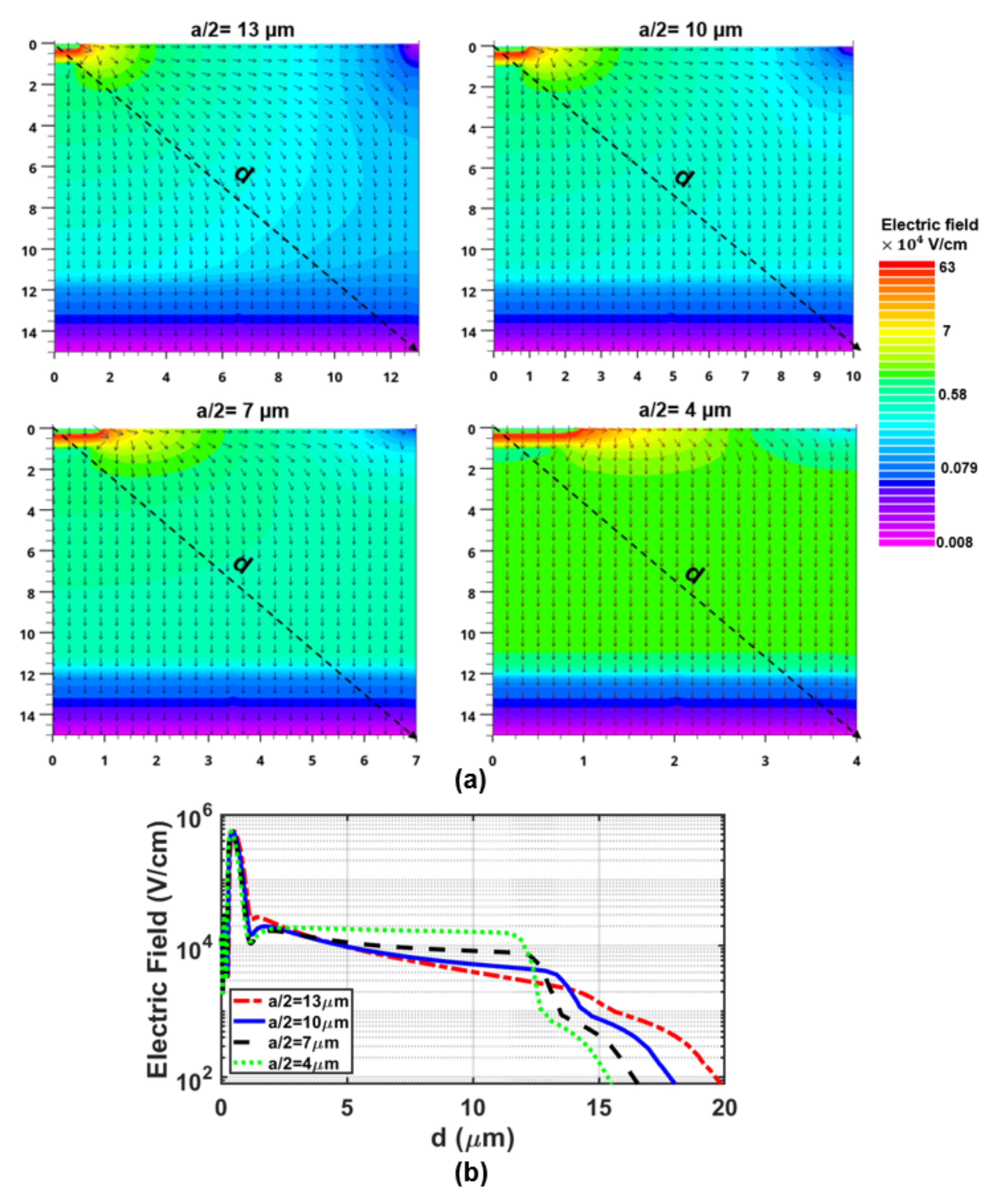
We used TCAD simulations with ATLAS to estimate an optimal array pitch size (a) of the MD-APD. It should be noted that we could not simulate the whole structure of the MD-APD because it requires a 3d simulation. Simulations with Cartesian coordinates are performed for a 2d cross-section indicated in
Figure 4b, which contains a half-cathode dot at the corner of a half-pitch-wide region.
Figure 6 illustrates the electric field distribution for different pitch sizes
a of 13, 10, 7, and 4 μm. These chosen simulation regions are sufficient because of symmetry reasons and boundary conditions of the simulator.
According to the electric field vector arrows, the electric field extends along the surface and then down towards the substrate. It is visualized that the strength of the electric field distributed across the detection zone decreases when the pitch size increases. It can be seen in
Figure 6b that the electric field strength at a “diagonal” distance
d of 10 μm from the origin of coordinates in the structure with a half pitch size of 4, 7, 10, and 13 μm are 16.3 kV/cm, 8.4 kV/cm, 5.3 kV/cm, and 4 kV/cm, respectively. A higher electric field distributed across the detection region in smaller structures is expected to provide faster carrier drift transfer and thus lead to a higher bandwidth.
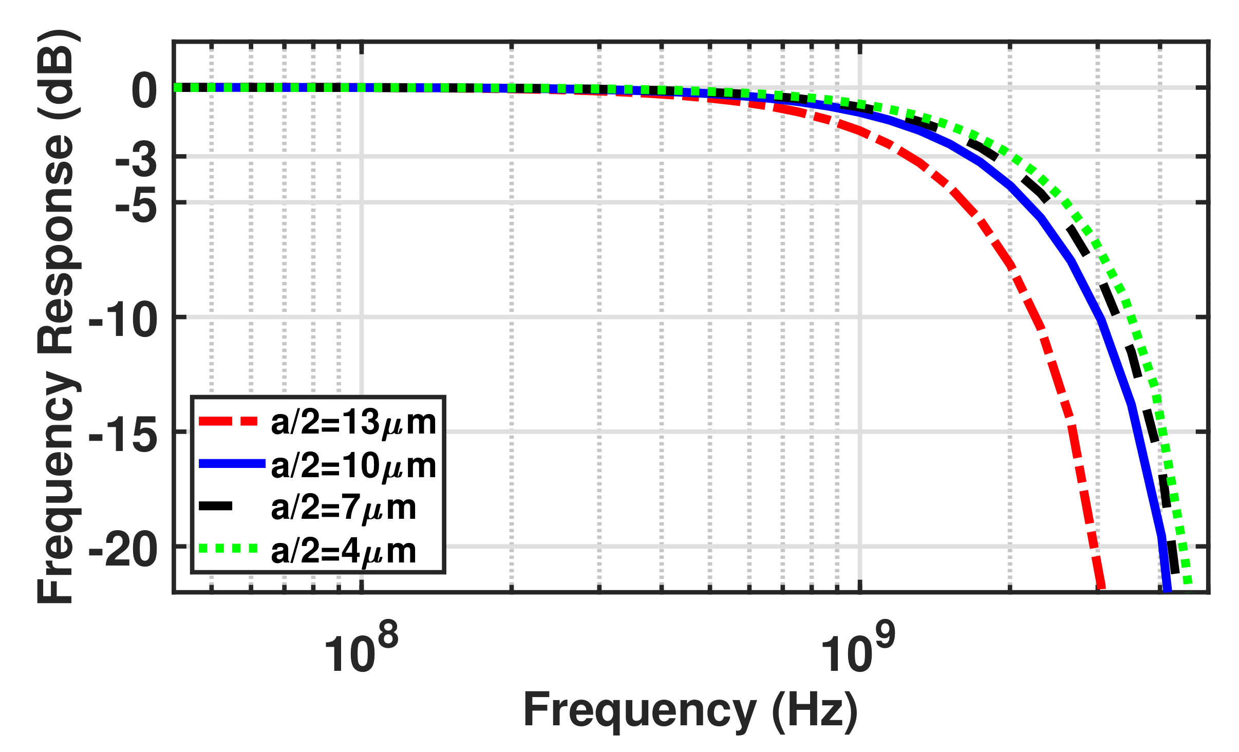
Figure 7 shows the normalized frequency responses for the different half pitch sizes of 13, 10, 7, and 4 μm, at a wavelength of 675 nm and a gain of 40, obtained from TCAD simulations.
Figure 7 demonstrates that a higher bandwidth is achieved by shrinking the distance between cathode dots because of the electron drift time reduction due to the shortening of the radial carrier drift distance and an increase in the electric field strength distributed across the detection zone. It is shown that the structures with an
a/2 of 13, 10, 7, and 4 μm achieve the bandwidth of 1.25 GHz, 1.7 GHz, 1.85 GHz, and 2 GHz, respectively. Taking a closer look at the dependence of the bandwidth on the cathode dots distance, it can be seen that reducing the
a/2 from 13 μm to 10 μm increases the bandwidth from 1.25 GHz to 1.7 GHz, while further reducing the distance provides less bandwidth improvement. This is due to the fact that in smaller structures, the
a/2 is smaller than the depth of the structure, and hence the vertical carriers’ transition from the deep depth (12 μm) limits the bandwidth, and therefore a further reduction of cathode dot distance has less influence on the bandwidth.
Now, the MD-APD can be designed according to TCAD simulation results and the above discussions. In the MD-APD design, a point that should be taken into account is that the bandwidth is limited by photo-generated carriers in the region between two adjacent cathode dots in the diagonal direction because it gives the longest drift distance (see
Figure 5). The longest lateral drift distance along the silicon surface is
. Here, the array pitch size of
a = 14 μm is selected for the MD-APD structure in which the distance between two adjacent diagonal cathode dots is 20 μm. According to the simulated frequency response results for different distances of the cathode dots, it is expected that the MD-APD achieves a bandwidth between 1.7 GHz and 1.85 GHz, corresponding to
a/2 = 7 μm and
a/2 = 10 μm, respectively. Because carriers generated between two adjacent dots on the horizontal/vertical axis (
a/2 = 7 μm) with a shorter drift distance and carriers generated in the area between two adjacent dots on the diagonal axis (
= 10 μm) with a longer drift distance contribute to the current flow (see
Figure 5), so, the pitch
a should be 14 μm. In the case where the pitch size of the array is
a = 20 μm, the bandwidth reduction due to carrier transfer between diagonal cathodes is remarkable (see curve corresponds to
a/2 = 13 μm from
Figure 7) and thus the overall bandwidth significantly decreases. Therefore, an MD-APD shown in
Figure 4 consisting of an array of 5 × 5 cathode dots with a pitch size of 14 μm can achieve a high bandwidth while providing an active area of 70 μm × 70 μm (exact active area: 5
−
4858 µm
2). However, MD-APDs with a smaller pitch size can achieve a slightly higher bandwidth, but at the cost of reducing the active area and increasing the capacitance.
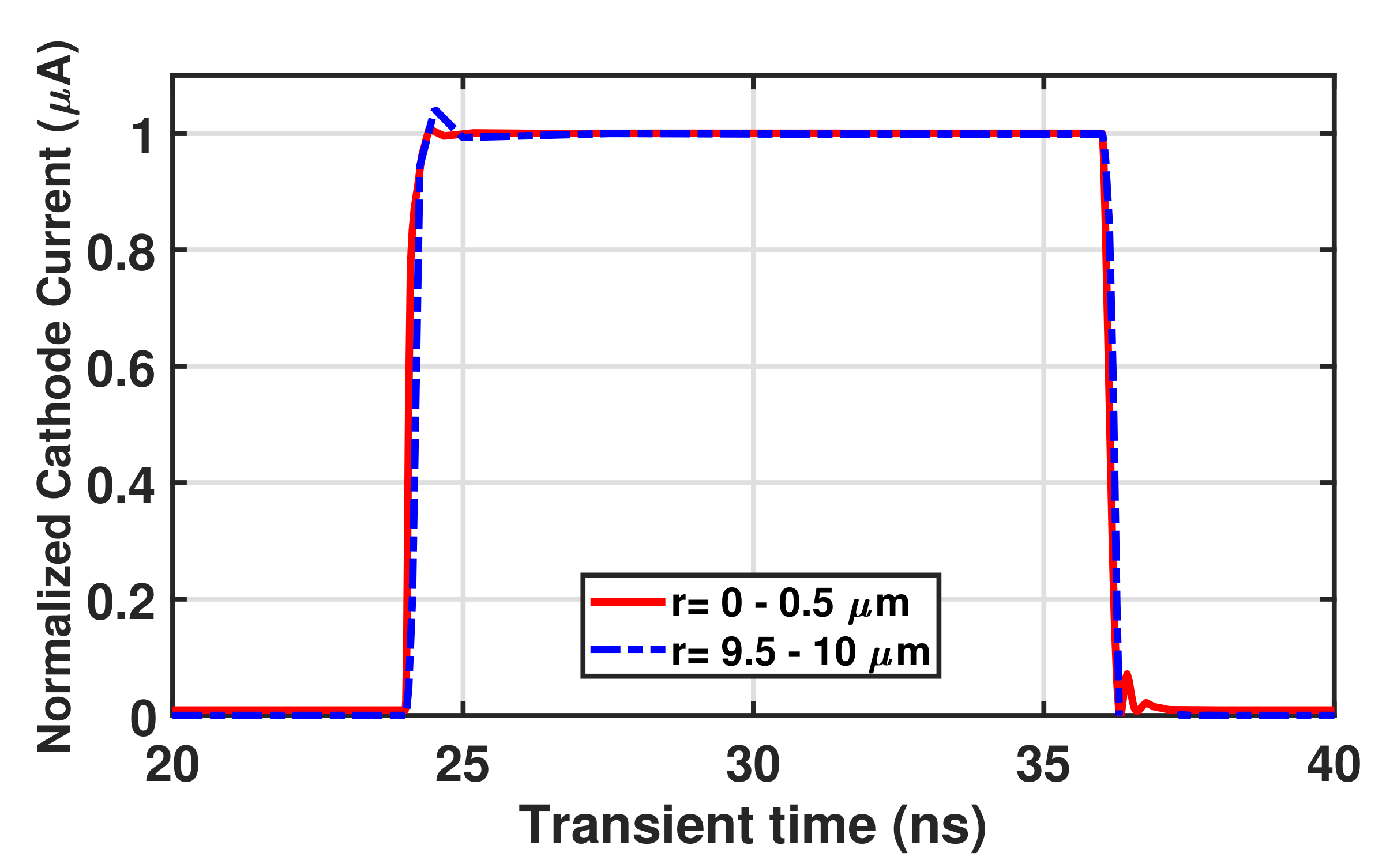
Since there are different drift carrier path lengths in the MD structure, we should care about the timing jitter performance evaluation of the MD-APD. However, accurately calculating the jitter based on the transit time is challenging due to the variations in the electric field strength along the carrier’s drift path. Therefore, we have conducted transient simulations under different conditions to estimate the largest possible jitter in the MD-APD. In the first simulation case, we have limited the incident light to the center of the structure (r = 0 to r = 0.5 μm), and therefore only the photogenerated carriers in the center reach the cathode with the shortest drift length. As a result, the rise time of the transient response corresponds to the shortest carrier transit time. The transient response (
Figure 8) for this condition shows a rise time of 160 ps. In the second simulation case, we have limited the light irradiation to the edge of the half diagonal of the MD diode (r = 9.5 μm to r = 10 μm; analogously to the frequency response simulations of the MD structure above), resulting only in the photogenerated carriers with the longest drift path reaching the cathode. Accordingly, the rise time of the transient response corresponds to the longest carrier transit time. A rise time of 240 ps is obtained from the transient response results in this condition (
Figure 8). The difference between these two values provides an estimation of the maximum jitter in the MD-APD, which is approximately 80 ps.
5. Discussion
The research work presented in this study focuses on the development of a dot avalanche photodiode (APD) that overcomes the trade-off between the light-sensitive area and capacitance of planar APDs commonly used in optical communication systems. One of the main challenges with planar APDs is the need to decouple the light-sensitive area from the P/N-junction area to reduce the capacitance while maintaining the light-sensitive area. The proposed dot APD achieves this by using the lateral distribution of the electric field throughout the diode, enabling vertical and peripheral charge collection.
The innovative aspect of this work lies in enlarging the light-sensitive area by expanding the cathode dot array by offering low capacitance. The base for this is the very low capacitance of a single-dot APD at a large light-sensitive area. The performance of the multi-dot APD compared with various Si CMOS APDs shows a significant improvement in the responsivity-bandwidth product (R-BW product) of 17.46 GHz, corresponding to the responsivity and bandwidth of R = 9.7 A/W and BW = 1.8 GHz, respectively. Additionally, the capacitance of the multi-dot APD is four times smaller than that of planar APDs, while maintaining a comparable active area. Furthermore, the multi-dot APD shows significant improvement in scalability and the ability to maintain its bandwidth and responsivity performance during up/down scaling.
It is worth emphasizing that the responsivity and frequency response of the MD-APD are independent of the array size but are affected by the array pitch size. This is due to the fact that the distribution of the electric field is independent of the number of cathodes in the array, but it changes with the change in the distance between the cathodes. However, the capacitance is proportional to the array size as the number of cathodes and metal connection length changes in different array sizes. In addition, as the drift path of carriers only depends on the array pitch size (i.e., shortest and longest paths) and is independent of the array size, the timing jitter is the same for different array sizes. Therefore, designing MD-APDs with different array sizes follows the same approach. This is one of the advantages of these structures, which makes it possible to easily expand the active area while maintaining the performance. These results demonstrate the superiority of the multi-dot APD over the state-of-the-art APDs and make it a promising candidate for a wide range of applications.
To better highlight, the contribution of this work over the state-of-the-art, the key performance parameters of the MD-APD are compared with various Si CMOS APDs and shown in
Table 1.

 ,
, 


