

A Temperature-to-Frequency Converter-Based On-Chip Temperature Sensor with an Inaccuracy of +0.65 °C/−0.49 °C
1
School of Microelectronics, Shanghai University, Shanghai 201800, China
2
The Shanghai Industrial μTechnology Research Institute, Shanghai 201899, China
*
Author to whom correspondence should be addressed.
Sensors 2023, 23(11), 5169; https://doi.org/10.3390/s23115169
Submission received: 27 March 2023
/
Revised: 26 May 2023
/
Accepted: 26 May 2023
/
Published: 29 May 2023
(This article belongs to the Section Industrial Sensors)
Abstract
:This paper proposes a temperature sensor based on temperature-frequency conversion using 180 nm CMOS technology. The temperature sensor consists of a proportional-to-absolute temperature (PTAT) current generating circuit, a relaxation oscillator with oscillation frequency proportional to temperature (OSC-PTAT), a relaxation oscillator with oscillation frequency independent of temperature (OSC-CON), and a divider circuit cascaded with D flip-flops. Using BJT as the temperature sensing module, the sensor has the advantages of high accuracy and high resolution. An oscillator that uses PTAT current to charge and discharge capacitors to achieve oscillation, and utilizes voltage average feedback (VAF) to enhance the frequency stability of the oscillator is tested. Through the dual temperature sensing process with the same structure, the influence of variables such as power supply voltage, device, and process deviation can be reduced to a certain extent. The temperature sensor in this paper was implemented and tested with a temperature measurement range of 0–100 °C, an inaccuracy of +0.65 °C/−0.49 °C after two-point calibration, a resolution of 0.003 °C, a resolution Figure of Merit (FOM) of 6.7 pJ/K2, an area of 0.059 mm2, and a power consumption of 32.9 μW.
1. Introduction
Over the past 50 years, the semiconductor industry has followed Moore’s Law [1]. With advances in process technology, the device size of circuits has continuously decreased, resulting in increased integration density of circuits within chips. The power density inside chips has also increased, leading to a rise in temperature during normal operation that affects the performance of the circuits [2]. Failure to dissipate heat normally can cause irreversible damage to the chip. Therefore, it is essential to incorporate temperature sensors into chips to monitor their temperature in real time [3].
Different types of sensors have their advantages and disadvantages, and the most suitable temperature sensor should be selected according to different application scenarios. Depending on the temperature sensing device, CMOS temperature sensors can be divided into BJT-type, resistor-type, full MOS transistor-type, and thermal diffusivity (TD) -type [4,5,6,7]. Based on the current mainstream architecture, on-chip integrated CMOS temperature sensors can be roughly divided into two categories: voltage-domain and time-domain temperature sensors. In brief, voltage-domain temperature sensors convert temperature into a corresponding voltage value using their temperature sensing module, and an analog-to-digital converter (ADC) is generally used to convert the voltage signal to a digital signal to transition from temperature to digital output. The specific selection of the ADC type generally depends on the temperature sensing module and system indicators. Time domain temperature sensors convert the voltage or current signal generated by the temperature sensing module into the time domain for processing, such as converting it into temperature-related frequency, period, or duty cycle, and then selecting the appropriate readout circuit to output digital encoding [8]. The different architectures lead to differences in the selection of the analog-to-digital conversion circuit, which directly affects the performance differences of CMOS temperature sensors. Voltage-domain CMOS temperature sensors often face problems such as complex structure, large area, and high power consumption due to the selection of ADCs. However, their accuracy is generally high. On the other hand, time-domain temperature sensors—as they select digital circuits such as time-to-digital converter (TDC) or frequency-to-digital converter (FDC) [9,10]—can often build most circuits using standard cell libraries, and have strong adaptability, simple structure, small area, and low power consumption. Therefore, it is necessary to determine CMOS temperature sensors with different architectures in advance according to different needs.
This article presents an on-chip temperature sensor with a temperature-frequency conversion mode, which can reduce the impact of some interference variables such as power supply voltage, device, and process deviations to a certain extent through a twin-temperature sensing process architecture with the same structure [11]. Based on the time domain, CMOS temperature sensors have a low accuracy and are susceptible to power supply voltage disturbances if external modules such as Low-dropout regulators (LDO) are not used due to their structure. Therefore, this architecture is one of the solutions to address the poor PV (Process-Voltage) characteristics of time-domain CMOS temperature sensors. The temperature sensor can achieve a temperature measurement range of 0–100 °C and, after a two-point calibration, the inaccuracy is +0.65 °C/−0.49 °C, the resolution is 0.003 °C, the area is 0.059 mm2, and the power consumption is 32.9 μW.
Section 1 introduces the type and application environment of on-chip temperature sensors and the advantages of this temperature sensor. Section 2 describes the circuit design principle of the temperature sensor. Section 3 presents the simulation results using simulation tools. Section 4 presents the test results after chip implementation. Finally, Section 5 provides a summary and conclusion.
2. Circuit Design of Temperature Sensor
2.1. Top-Level Architecture
Figure 1 depicts a block diagram of the on-chip temperature sensor principle. The temperature sensor consists of a current generating circuit that is proportional to the absolute temperature, a relaxation oscillator with oscillation frequency proportional to temperature (OSC-PTAT), a relaxation oscillator with oscillation frequency independent of temperature (OSC-CON), and a frequency-to-digital converter circuit. The PTAT current is generated by the temperature sensing circuit and used to charge the OSC-CON and OSC-PTAT modules. The OSC-CON module produces a reference clock independent of temperature, while the OSC-PTAT module generates a clock signal with frequency proportional to temperature. Two digital converters count the signals generated by the two modules, respectively. Both frequency-to-digital converters are controlled by an enable signal for simultaneous counting. When the digital converter of the OSC-CON module reaches its maximum count, it stops counting and triggers the digital converter of the OSC-PTAT module to stop counting as well. At this point, the OSC-PTAT outputs a binary code word proportional to temperature.
2.2. PTAT Current Circuit
The temperature sensing circuit transmits temperature by observing the characteristic of the junction voltage of BJT with temperature variation. Using BJT as the temperature sensing module has the advantages of high precision and high resolution. As shown in Figure 2, PNP triodes, and are connected as diodes, because the number of parallel transistors in two PNP transistors is different, the voltage on is , the voltage on is , and the voltage on resistor is the voltage difference of two PNP transistors, , which can be calculated by Equation (2). It is a voltage proportional to temperature, and divided by yields a current proportional to temperature [12]. Table 1 shows the CMOS parameters of the PTAT current generation circuit.
Here, q represents the electronic charge, k is the Boltzmann constant, IC and IS are, respectively, the collector and saturation currents of the PNP, T is the absolute temperature, and n represents the number of transistors in parallel with . In order to achieve circuit matching, the circuit in this paper was designed with n = 8.
2.3. Principles of OSC Circuit Design
Common oscillation methods include crystal oscillators, traditional RC oscillators, traditional oscillators that use PTAT current to charge and discharge capacitors for oscillation, bandgap-reference ring oscillators, bandgap-reference relaxation oscillators, and hybrid oscillators with peak-holding feedback of both relaxation and ring types [13,14,15,16,17]. However, all of the aforementioned oscillation methods have certain drawbacks. The frequency variation of waveforms generated by crystal oscillators is on the order of ppm, but they are costly and cannot be integrated into a chip. The oscillation frequency variation caused by the circuit structure of traditional RC oscillators, traditional oscillators that use PTAT current to charge and discharge capacitors for oscillation, bandgap-reference ring oscillators, bandgap-reference relaxation oscillators, and hybrid oscillators with peak-holding feedback of both relaxation and ring types exceeds ±1% with changes in voltage and temperature.
In traditional oscillator circuits that use PTAT current to charge and discharge capacitors to achieve oscillation, variations in the delay of comparators and RS flip-flops result in frequency changes with respect to voltage and temperature. The aging of current sources can degrade the accuracy of the slope and cause frequency changes. The flicker noise of current sources accumulates jitter. This paper introduces the concept of Voltage Average Feedback (VAF) [18], proposes oscillators’ structure with VAF, and implements oscillation by charging and discharging capacitors with PTAT current—as shown in Figure 3—to adjust the output voltage of the VAF circuit based on the size of the delay time of comparators and RS flip-flops, thereby achieving oscillator stability independent of comparator and RS flip-flop delays, and eliminating cumulative jitter in the circuit. When the temperature varies from 0 to 100 °C, the output frequency of the oscillator changes by 0.08%, thereby improving the frequency stability of the relaxation oscillator.
Taking OSC-PTAT as an example, the mechanism of the oscillation waveform generation is described as shown in Figure 3a: Assuming that the RS trigger composed of the NAND gate is in the reset state, when R = “1” and S = “0”, Q outputs “0” and Q’ outputs “1“, M1, M5, M6, and M7 are cut off while M2, M3, M4, and M8 are turned on, and the left comparator circuit of the circuit works. The current source charges capacitor C1, causing to rise, and is transmitted as to the reverse input of the VAF circuit. The right comparator circuit of the circuit does not work, and the output is 0 V. At the same time, when the circuit starts to work, the active filter composed of R3 and C3 makes the output voltage a constant value. When exceeds , the left comparator outputs “0”, while the right comparator still outputs “1”. At this time, R = “0” and S = “1”, the RS trigger is in the set state, Q outputs “1”, Q’ outputs “0”, M1, M5, M6, and M7 are turned on while M2, M3, M4, and M8 are cut off, and the right comparator circuit of the circuit works. The current source charges capacitor C2, causing to rise, and is transmitted as to the negative input of the VAF circuit. The left comparator circuit of the circuit does not work, and the output is 0 V. When exceeds , the RS trigger returns to the reset state. Therefore, the RS trigger is always in the alternating state of reset and set, and the waveforms of and alternately transmit to the reverse output of the VAF circuit, thereby generating a stable oscillation waveform. Similarly, the oscillation mechanism of OSC-CON is roughly the same as that of OSC-PTAT, so it is not repeated here.
Temperature-to-frequency conversion in OSC:
By substituting Equation (3) into Equation (5), the following expression is obtained:
As shown in Figure 3a, , which can be substituted into the above equation to obtain a signal oscillation frequency that is directly proportional to the temperature for the OSC-PTAT circuit. As shown in Figure 3b, , which can be substituted into the above equation to obtain a signal oscillation frequency that is independent of temperature for the OSC-CON circuit.
The circuit diagrams of the operational amplifier and the comparator in both the OSC-PTAT and OSC-CON circuits are presented in Figure 4a and b, respectively. The operational amplifier uses a symmetric OTA (Operational Transconductance Amplifier) architecture, providing higher bandwidth. The comparator uses a two-stage operational amplifier structure, offering elevated DC gain. Table 2 and Table 3 show the parameters of the CMOS transistors in operational amplifiers and some performance indicators of operational amplifiers, and the parameters of the CMOS transistors in comparators and some performance indicators of comparators, respectively.
2.4. Frequency-to-Digital Converter
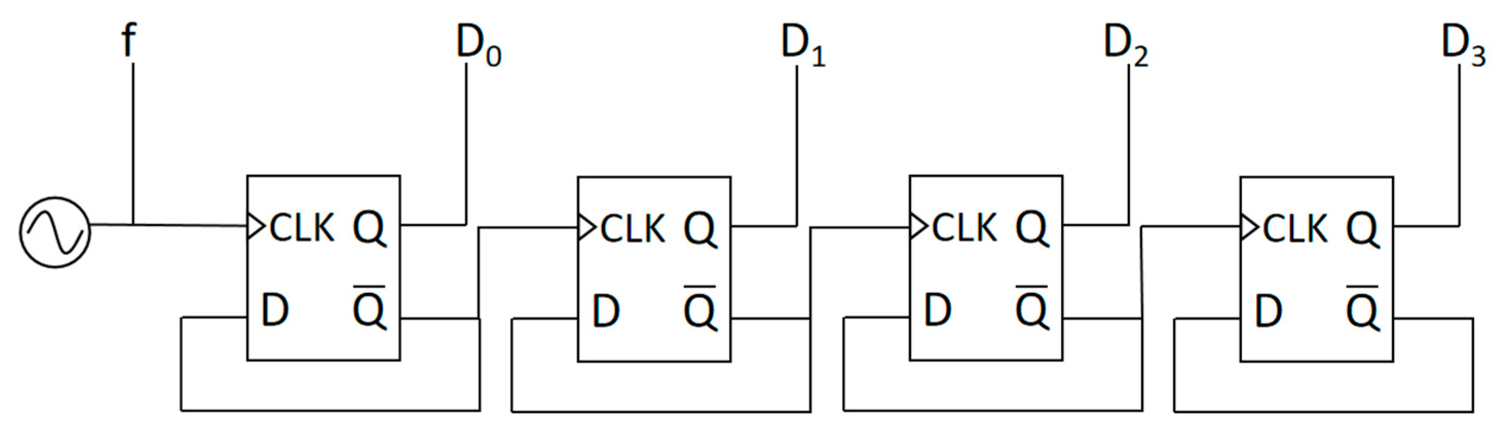
The square wave signals generated by OSC-PTAT and OSC-CON are, respectively, input into cascaded D flip-flops shown in Figure 5 as the clock signal of the first D flip-flop. When a clock pulse arrives, the first D flip-flop sends the D input data to the Q output and the inverted data of Q to the Q’ output, which serves as the clock signal of the next stage D flip-flop. The same process is repeated for the next clock pulse, but with the input data already inverted. This results in the Q output changing its state every two clock pulses, achieving a halving of the frequency. By cascading D flip-flops, a frequency divider circuit is implemented which converts the signal frequency into a binary counting function. The counting value of OSC-CON is taken as a reference to observe the counting value of OSC-PTAT at this time.
The designed counter in this paper is 16-bit, and a 4-bit counter is taken as an example to explain the principle of circuit counting. The square wave signals generated by OSC-CON and OSC-PTAT are input into the digital frequency converter and the outputs are DC [0]-DC [3] and DP [0]-DP [3], respectively. Since the output frequency of the OSC-CON signal is independent of temperature, the counting time is fixed when the number of counting bits is determined. The 4-bit overflow value of DC [0]-DC [3] is taken as the counting reference to observe the counting value of DP [0]-DP [3]. DP is output in 4-bit binary complement form, and its value is exactly the difference between the two counters. Finally, the corresponding decimal number of DP [0]-DP [3] and the temperature are in a first-order linear relationship.
3. Simulation Results
The circuit design was implemented using the SMIC 180 nm mixed signal CMOS technology in Cadence 6.17, and the circuit was simulated using the spectre tool. Under the TT process corner, Figure 6a shows that the PTAT current output of the temperature sensing circuit is proportional to the temperature ranging from 0 °C to 100 °C. Figure 6b shows that, as the temperature varies from 0 °C to 100 °C, the frequency of remains relatively constant, while the frequency of varies in direct proportion to the temperature. The output code is proportional to the temperature.
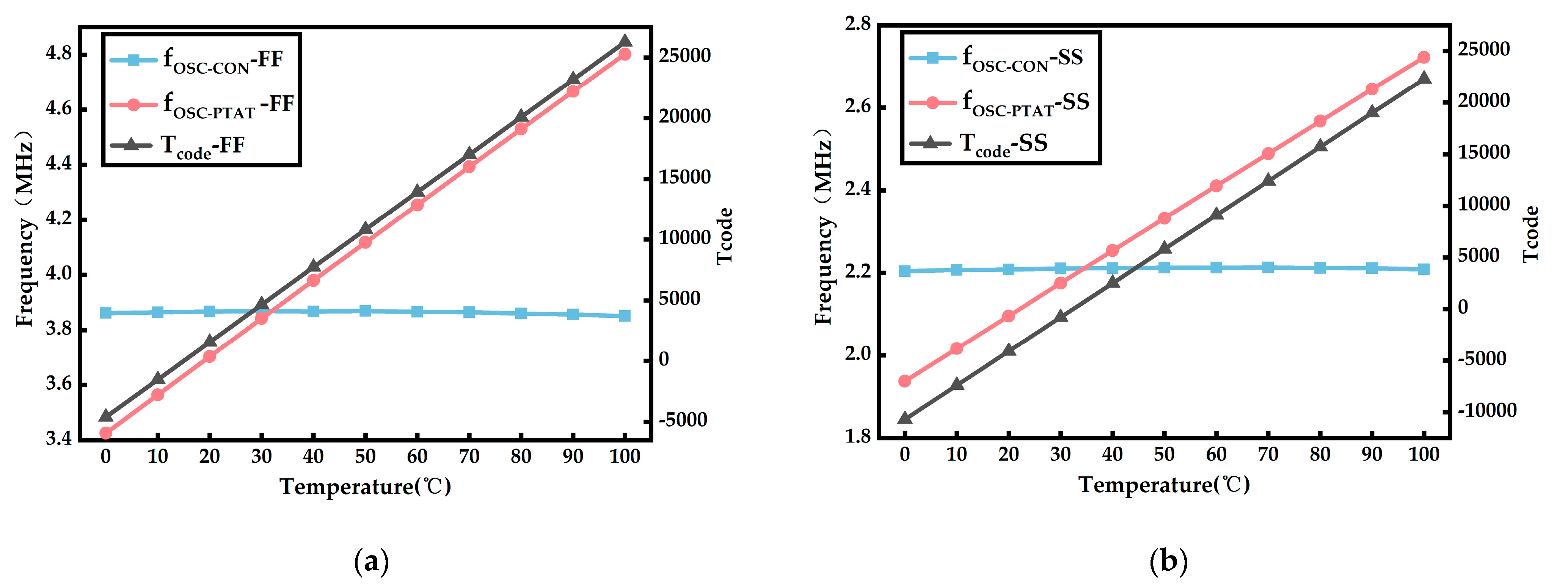
As shown in Figure 7, the outputs of , , and change as the temperature changes from 0 °C to 100 °C for the FF and SS process corners.
As shown in Figure 8, the temperature measurement error of the temperature sensor is evaluated when the temperature is varied from 0 to 100 °C under different process corners; namely TT, SS, and FF. At 40 °C, the temperature measurement error of the temperature sensor under various corners varies at different supply voltages of 1.5–1.8 V.
The circuit is subjected to five Monte Carlo simulations with temperature information added under the TT process corner. The result after two-point calibration is shown in Figure 9.
4. Test Results
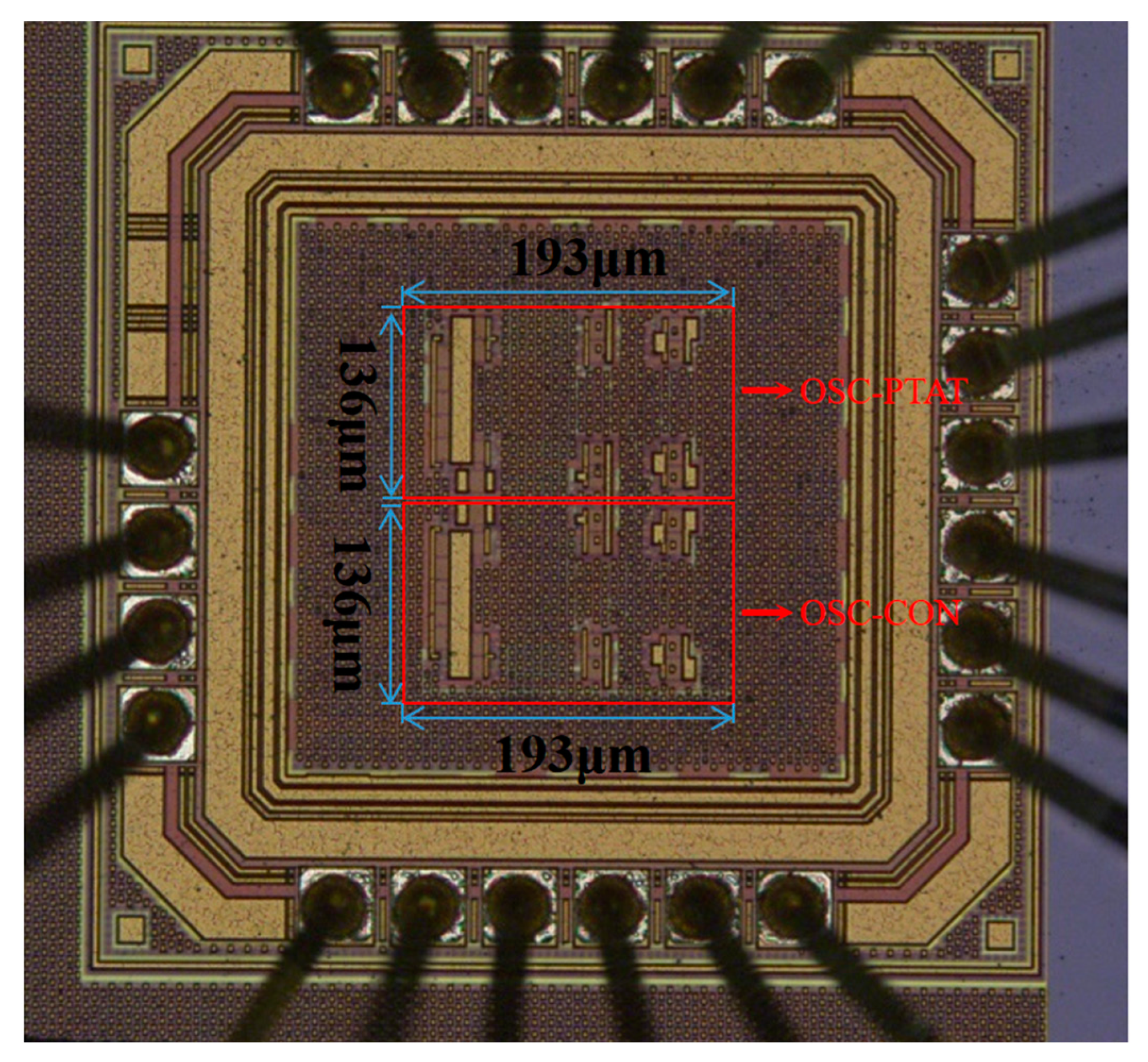
The on-chip temperature sensor proposed in this paper was designed and implemented in SMIC standard 180 nm CMOS process. The core area of the circuit was 0.059 mm2, as shown in the microphotograph in Figure 10.
Five test chips were packaged in QFN and tested in high and low temperature chambers. Among them, DS18B20 was used for chip reference temperature measurement to obtain sufficient accuracy of the temperature of the chip environment. At the same time, a single-chip microcontroller development board was used to obtain and record the output code words. The operating voltage was 1.5 V, the temperature measurement range was 0–100 °C, and the temperature measurement step was 10 °C. Figure 11 shows the temperature of the test signal and the final output code word for the five chips. The output frequency of the chip test is linearly related to the temperature, and the output code word range is approximately −10688 to 26266 for a temperature range of 0–100 °C, corresponding to a resolution of 0.003 °C.
As shown in Figure 12, five temperature sensor chips were tested. The final output code is a function of temperature: . Then, the output signal amplitude under any two temperature points (, ) is determined, assuming that the temperature measurement error is 0 at these two points. This determines the coordinates of the two points, which are used to obtain the calibrated “ideal curve”. Finally, the temperature measurement error at each point can be obtained based on the definition of temperature measurement error. By performing two-point calibration, the temperature measurement error is within +0.65 °C/−0.49 °C.
Table 4 summarizes the performance parameters of the CMOS temperature sensor designed in this paper and compares them with the performance of other sensors.
5. Conclusions
In this paper, we have presented an on-chip temperature sensor based on temperature-frequency conversion for real-time temperature monitoring of the chip. By using BJT for temperature sensing, VAF for debouncing, and a dual-sensing process architecture, the impact of variables such as power supply voltage, device, and process deviations have been reduced, generating a stable oscillation frequency. Finally, the signal frequency is converted into binary numbers by a frequency-to-digital converter. The temperature sensor was tested after being fabricated using a 180 nm CMOS process with a temperature measurement range of 0°C–100°C, a resolution of 0.003°C, an area of 0.465 mm2, a power consumption of 32.9 μW, a conversion time of 22.75 ms, a resolution of 0.003 °C, a resolution FOM of 6.7 pJ/K2, and an accuracy after two-point calibration of +0.65 °C/−0.49 °C. The proposed design has addressed the problem of low accuracy in traditional temperature-frequency conversion-based temperature sensors.
Author Contributions
Conceptualization, Z.X. and L.Y.; methodology, Z.X., L.Y. and X.Z.; software, Z.X. and X.Z.; validation, Z.X., L.Y. and S.C.; formal analysis, Z.X. and J.C.; investigation, Z.X. and L.Y.; resources, Z.X.; data curation, Z.X. and S.C.; writing—original draft preparation, Z.X.; writing—review and editing, L.Y. and J.C.; visualization, Z.X.; supervision, L.Y., J.C. and X.Z.; project administration, L.Y.; funding acquisition, L.Y. All authors have read and agreed to the published version of the manuscript.
Funding
This research is funded by the National Key R&D Program of China Grants 2021YFB3200600 and 2021YFB3200602.
Institutional Review Board Statement
Not applicable.
Informed Consent Statement
Not applicable.
Data Availability Statement
Not applicable.
Conflicts of Interest
The authors declare no conflict of interest.
References
- Xiu, L. Time Moore: Exploiting Moore’s Law from The Perspective of Time. IEEE Solid-State Circuits Mag. 2019, 11, 39–55. [Google Scholar] [CrossRef]
- Samake, A.; Kocanda, P.; Kos, A. A New Idea of Effective Cooling of Integrated Circuits. In Proceedings of the 2016 International Conference on Signals and Electronic Systems (ICSES), Krakow, Poland, 5–7 September 2016; IEEE: Krakow, Poland, 2016; pp. 179–182. [Google Scholar]
- Matsuda, T.; Yamada, K.; Demachi, H.; Iwata, H.; Hatakeyama, T.; Ishizuka, M.; Ohzone, T. Analysis of Temperature Distribution in Stacked IC With On-Chip Sensing Device Arrays. IEEE Trans. Semicond. Manufact. 2015, 28, 213–220. [Google Scholar] [CrossRef]
- Souri, K.; Chae, Y.; Makinwa, K.A.A. A CMOS Temperature Sensor with a Voltage-Calibrated Inaccuracy of ±0.15 °C (3σ) from −55 °C to 125 °C. IEEE J. Solid-State Circuits 2013, 48, 292–301. [Google Scholar] [CrossRef]
- Ikegami, A.; Arima, H.; Tosaki, H.; Matsuoka, Y.; Mitsuro, A.; Minorikawa, H.; Asahino, Y. Thick-Film Thermistor and Its Applications. IEEE Trans. Comp. Hybrids Manufact. Technol. 1980, 3, 541–550. [Google Scholar] [CrossRef]
- Xie, S.; Theuwissen, A. All-MOS Self-referenced Temperature Sensor. Electron. Lett. 2019, 55, 1045–1047. [Google Scholar] [CrossRef]
- Sonmez, U.; Sebastiano, F.; Makinwa, K.A.A. Compact Thermal-Diffusivity-Based Temperature Sensors in 40-Nm CMOS for SoC Thermal Monitoring. IEEE J. Solid-State Circuits 2017, 52, 834–843. [Google Scholar] [CrossRef]
- Souri, K.; Chae, Y.; Thus, F.; Makinwa, K. 12.7 A 0.85V 600nW All-CMOS Temperature Sensor with an Inaccuracy of ±0.4 °C (3σ) from −40 to 125 °C. In Proceedings of the 2014 IEEE International Solid-State Circuits Conference Digest of Technical Papers (ISSCC), San Francisco, CA, USA, 9–13 February 2014; IEEE: San Francisco, CA, USA, 2014; pp. 222–223. [Google Scholar]
- Tan, Y.; Liu, Z.; Hao, X.; Shen, Z.; Jiang, H.; Tian, F.; Liu, J. A 1.3-ΜW −0.3/+0.27 °C Inaccuracy Fully-Integrated Temperature Sensor Based on a Pre-Charge Relaxation Oscillator for IoT Applications. In Proceedings of the 2019 IEEE Asia-Pacific Microwave Conference (APMC), Singapore, 10–13 December 2019; IEEE: Singapore, 2019. [Google Scholar]
- Yang, W.; Jiang, H.; Wang, Z.; Jia, W. An Ultra-Low Power Temperature Sensor Based on Relaxation Oscillator in Standard CMOS. In Proceedings of the 2018 IEEE International Conference on Electron Devices and Solid State Circuits (EDSSC), Shenzhen, China, 6–8 June 2018; IEEE: Shenzhen, China, 2018; pp. 1–2. [Google Scholar]
- Someya, T.; Islam, A.K.M.M.; Sakurai, T.; Takamiya, M. An 11-NW CMOS Temperature-to-Digital Converter Utilizing Sub-Threshold Current at Sub-Thermal Drain Voltage. IEEE J. Solid-State Circuits 2019, 54, 613–622. [Google Scholar] [CrossRef]
- Szajda, K.S.; Sodini, C.G.; Bowman, H.F. A Low Noise, High Resolution Silicon Temperature Sensor. IEEE J. Solid-State Circuits 1996, 31, 1308–1313. [Google Scholar] [CrossRef]
- O’Shaughnessy, T. A CMOS, Self Calibrating, 100 MHz RC-Oscillator for ASIC Applications. In Proceedings of the Eighth International Application Specific Integrated Circuits Conference, Austin, TX, USA, 18–22 September 1995; IEEE: Austin, TX, USA, 1995; pp. 279–282. [Google Scholar]
- Aita, A.L.; De la Cruz, J.V.; Bashirullah, R. A 0.45V CMOS Relaxation Oscillator with ±2.5% Frequency Stability from −55 °C to 125 °C. In Proceedings of the 2015 IEEE International Symposium on Circuits and Systems (ISCAS), Lisbon, Portugal, 24–27 May 2015; IEEE: Lisbon, Portugal, 2015; pp. 493–496. [Google Scholar]
- Sundaresan, K.; Allen, P.E.; Ayazi, F. Process and Temperature Compensation in a 7-MHz CMOS Clock Oscillator. IEEE J. Solid-State Circuits 2006, 41, 433–442. [Google Scholar] [CrossRef]
- Vilas Boas, A.; Olmos, A. A Temperature Compensated Digitally Trimmable On-Chip IC Oscillator with Low Voltage Inhibit Capability. In Proceedings of the 2004 IEEE International Symposium on Circuits and Systems (IEEE Cat. No.04CH37512), Vancouver, BC, Canada, 23–26 May 2004; IEEE: Vancouver, BC, Canada, 2004; pp. 501–504. [Google Scholar]
- Lasanen, K.; Raisanen-Ruotsalainen, E.; Kostamovaara, J. A 1-V, Self Adjusting, 5-MHz CMOS RC-Oscillator. In Proceedings of the 2002 IEEE International Symposium on Circuits and Systems. Proceedings (Cat. No.02CH37353), Phoenix-Scottsdale, AZ, USA, 7 August 2002; IEEE: Phoenix-Scottsdale, AZ, USA, 2002; Volume 4, pp. 377–380. [Google Scholar]
- Tokunaga, Y.; Sakiyama, S.; Matsumoto, A.; Dosho, S. An On-Chip CMOS Relaxation Oscillator with Voltage Averaging Feedback. IEEE J. Solid-State Circuits 2010, 45, 1150–1158. [Google Scholar] [CrossRef]
- Yousefzadeh, B.; Makinwa, K.A.A. A BJT-Based Temperature-to-Digital Converter With a ±0.25 °C 3σ -Inaccuracy from −40 °C to +180 °C Using Heater-Assisted Voltage Calibration. IEEE J. Solid-State Circuits 2019, 55, 369–377. [Google Scholar] [CrossRef]
- Qin, C.; Huang, Z.; Liu, Y.; Li, J.; Lin, L.; Tan, N.; Yu, X. An Energy-Efficient BJT-Based Temperature Sensor with ±0.8 °C (3σ) Inaccuracy from −50 to 150 °C. Sensors 2022, 22, 9381. [Google Scholar] [CrossRef] [PubMed]
- Wang, X.; Wang, P.-H.P.; Cao, Y.; Mercier, P.P. A 0.6 V 75 nW All-CMOS Temperature Sensor with 1.67 m°C/MV Supply Sensitivity. IEEE Trans. Circuits Syst. I 2017, 64, 2274–2283. [Google Scholar] [CrossRef]
- Jeong, S.; Foo, Z.; Lee, Y.; Sim, J.-Y.; Blaauw, D.; Sylvester, D. A Fully-Integrated 71 NW CMOS Temperature Sensor for Low Power Wireless Sensor Nodes. IEEE J. Solid-State Circuits 2014, 49, 1682–1693. [Google Scholar] [CrossRef]
- Li, J.; Lin, Y.; Ning, N.; Yu, Q. A +0.44 °C/−0.4 °C Inaccuracy Temperature Sensor with Multi-Threshold MOSFET-Based Sensing Element and CMOS Thyristor-Based VCO. IEEE Trans. Circuits Syst. 2020, 68, 1102–1113. [Google Scholar] [CrossRef]
- Yang, W.; Jiang, H.; Wang, Z. A 0.0014 Mm2 150 NW CMOS Temperature Sensor with Nonlinearity Characterization and Calibration for the −60 to +40 °C Measurement Range. Sensors 2019, 19, 1777. [Google Scholar] [CrossRef] [PubMed]
- Tang, Z.; Fang, Y.; Yu, X.-P.; Shi, Z.; Tan, N. A CMOS Temperature Sensor with Versatile Readout Scheme and High Accuracy for Multi-Sensor Systems. IEEE Trans. Circuits Syst. 2018, 65, 3821–3829. [Google Scholar] [CrossRef]
- Chuang, M.-C.; Tai, C.-L.; Hsu, Y.-C.; Roth, A.; Soenen, E. A Temperature Sensor with a 3 Sigma Inaccuracy of ±2 °C without Trimming from −50 °C to 150 °C in a 16 nm FinFET Process. In Proceedings of the ESSCIRC Conference 2015—41st European Solid-State Circuits Conference (ESSCIRC), Graz, Austria, 14–18 September 2015; IEEE: Graz, Austria, 2015; pp. 271–274. [Google Scholar]
Figure 1.
Block diagram of the temperature sensing principle of the temperature sensor.

Figure 2.
PTAT current circuit of temperature sensor.

Figure 3.
The circuit diagrams of relaxation oscillators. (a) The circuit diagram of a relaxation oscillator with oscillation frequency proportional to temperature (OSC-PTAT). (b) The circuit diagram of a relaxation oscillator with oscillation frequency independent of temperature (OSC-CON).
Figure 3.
The circuit diagrams of relaxation oscillators. (a) The circuit diagram of a relaxation oscillator with oscillation frequency proportional to temperature (OSC-PTAT). (b) The circuit diagram of a relaxation oscillator with oscillation frequency independent of temperature (OSC-CON).

Figure 4.
Operational amplifiers and comparators in the OSC-PTAT and OSC-CON circuits. (a) Circuit diagram of the operational amplifier. (b) Circuit diagram of the comparator.
Figure 4.
Operational amplifiers and comparators in the OSC-PTAT and OSC-CON circuits. (a) Circuit diagram of the operational amplifier. (b) Circuit diagram of the comparator.

Figure 5.
Cascaded D flip-flops are used to implement circuit counting.

Figure 6.
Under the TT process corner, the simulation results of the circuit when temperature varies from 0 to 100 °C. (a) Graph of the relationship between output current of the bias circuit and temperature. (b) The variation of , , and with temperature.
Figure 6.
Under the TT process corner, the simulation results of the circuit when temperature varies from 0 to 100 °C. (a) Graph of the relationship between output current of the bias circuit and temperature. (b) The variation of , , and with temperature.

Figure 7.
Variation of parameters at different process angles. (a) Under the FF process corner. (b) Under the SS process corner.
Figure 7.
Variation of parameters at different process angles. (a) Under the FF process corner. (b) Under the SS process corner.

Figure 8.
The temperature measurement error of the temperature sensor. (a) The temperature error curves of the temperature sensor under various corners. (b) At 40 °C, the temperature measurement error of the temperature sensor under various corners.
Figure 8.
The temperature measurement error of the temperature sensor. (a) The temperature error curves of the temperature sensor under various corners. (b) At 40 °C, the temperature measurement error of the temperature sensor under various corners.

Figure 9.
The Monte Carlo simulation temperature error after two-point calibration.

Figure 10.
Microphotograph of the temperature sensor chip.

Figure 11.
The temperature and output code of five test chips.

Figure 12.
Temperature measurement error of the chip after two-point calibration.


Table 1.
Parameters of the CMOS transistors in the PTAT current circuit.
| CMOS Parameters | |||
|---|---|---|---|
| Instance Name | W (μm)/ L (μm) | Finger | Multiplier |
| M1, M2 | 1/4 | 1 | 2 |
| M3, M4, M5, M6, M9, M10 | 2/4 | 1 | 2 |
| M7, M8, M11, M12 | 2/4 | 1 | 8 |
Table 2.
The parameters of the CMOS transistors in the operational amplifier and performance indicators of the operational amplifier.
Table 2.
The parameters of the CMOS transistors in the operational amplifier and performance indicators of the operational amplifier.
| CMOS Parameters | |||
|---|---|---|---|
| Instance Name | W (μm)/ L (μm) | Finger | Multiplier |
| M1, M2 | 1/0.5 | 1 | 2 |
| M3, M4, M5, M6 | 1/1 | 1 | 2 |
| M7, M9 | 2/1 | 1 | 2 |
| M8 | 2/1 | 1 | 4 |
| M10 | 2/1 | 1 | 2 |
| Circuit Performance Parameters | |||
| Gain (G) | 42 dB | ||
| 3 dB Bandwidth (BW) | 615 kHz | ||
| Phase margin (PM) | 56 deg | ||
Table 3.
The parameters of the CMOS transistors in the comparator and performance indicators of the comparator.
Table 3.
The parameters of the CMOS transistors in the comparator and performance indicators of the comparator.
| CMOS Parameters | |||
|---|---|---|---|
| Instance Name | W (μm)/ L (μm) | Finger | Multiplier |
| M1, M2, M3, M4, M5 | 2/4 | 1 | 2 |
| M6 | 4/4 | 1 | 2 |
| M7 | 4/4 | 1 | 4 |
| M8 | 4/4 | 1 | 1 |
| Circuit Performance Parameters | |||
| Gain (G) | 81.4 dB | ||
| 3 dB Bandwidth (BW) | 43.1 kHz | ||
Table 4.
Comparison of performance parameters for CMOS temperature sensors.
| Parameters | [19] | [20] | [21] | [22] | [23] | [24] | [25] | [26] | This Work |
|---|---|---|---|---|---|---|---|---|---|
| Technology | 160 nm | 180 nm | 180 nm | 180 nm | 130 nm | 130 nm | 130 nm | 16 nm | 180 nm |
| type | CMOS | CMOS | CMOS | CMOS | CMOS | CMOS | CMOS | FinFET | CMOS |
| Area (mm2) | 0.15 | 0.13 | 0.45 | 0.09 | 0.07 | 0.0014 | 0.29 | 0.0126 | 0.059 |
| Supply (V) | 1.8 | 1.8/3.3 | 0.6 | 1.2 | 0.95 | 0.85 | 2–3.6 | 1.8 | 1.8 |
| Temp. range (°C) | −40–180 | −50–150 | 0–100 | 0–100 | 0–80 | −60–40 | −40–125 | −50–150 | 0–100 |
| Inaccuracy (°C) | ±0.2 | ±0.8 | +0.62/−1.33 | +1.5/−1.4 | +0.44/−0.4 | ±2 | ±0.47 | ±2 | +0.65/−0.49 |
| Calibration | 1-point | 1-point | 2-point | 2-point | 2-point | 2-point | 1-point | 0-point | 2-point |
| Resolution (°C) | 0.023 | 0.04 | 0.1 | 0.3 | 0.1 | 0.5 | 0.016 | 0.38 | 0.003 |
| Power (μW) | 9.7 | 45.7 | 0.075 | 0.071 | 0.196 | 0.15 | 313.5 | 1210 | 32.9 |
| Conversion rate (ms) | 20 | 10.24 | 254 | 30 | 59 | 1000 | 5.12 | 0.27 | 22.75 |
| Resolution *FOM (pJ/K2) | 103 | 748 | 190 | 190 | 120 | 37500 | 411 | 47175 | 6.7 |
[22].
Disclaimer/Publisher’s Note: The statements, opinions and data contained in all publications are solely those of the individual author(s) and contributor(s) and not of MDPI and/or the editor(s). MDPI and/or the editor(s) disclaim responsibility for any injury to people or property resulting from any ideas, methods, instructions or products referred to in the content. |
© 2023 by the authors. Licensee MDPI, Basel, Switzerland. This article is an open access article distributed under the terms and conditions of the Creative Commons Attribution (CC BY) license (https://creativecommons.org/licenses/by/4.0/).
Share and Cite
MDPI and ACS Style
Xu, Z.; Zhang, X.; Chen, S.; Cheong, J.; Yao, L. A Temperature-to-Frequency Converter-Based On-Chip Temperature Sensor with an Inaccuracy of +0.65 °C/−0.49 °C. Sensors 2023, 23, 5169. https://doi.org/10.3390/s23115169
AMA Style
Xu Z, Zhang X, Chen S, Cheong J, Yao L. A Temperature-to-Frequency Converter-Based On-Chip Temperature Sensor with an Inaccuracy of +0.65 °C/−0.49 °C. Sensors. 2023; 23(11):5169. https://doi.org/10.3390/s23115169
Chicago/Turabian StyleXu, Zicong, Xuan Zhang, Sili Chen, Jiahao Cheong, and Lei Yao. 2023. "A Temperature-to-Frequency Converter-Based On-Chip Temperature Sensor with an Inaccuracy of +0.65 °C/−0.49 °C" Sensors 23, no. 11: 5169. https://doi.org/10.3390/s23115169
Note that from the first issue of 2016, this journal uses article numbers instead of page numbers. See further details here.