Article

Synthesis of WS2 Ultrathin Films by Magnetron Sputtering Followed by Sulfurization in a Confined Space

National Institute of Materials Physics, Atomistilor 405A, 077125 Magurele, Romania
*
Author to whom correspondence should be addressed.
Surfaces 2024, 7(1), 108-119; https://doi.org/10.3390/surfaces7010008
Submission received: 7 January 2024 / Revised: 4 February 2024 / Accepted: 8 February 2024 / Published: 11 February 2024
(This article belongs to the Collection Featured Articles for Surfaces)

Abstract

:
In the quest for advanced materials suitable for next-generation electronic and optoelectronic applications, tungsten disulfide (WS2) ultrathin films have emerged as promising candidates due to their unique properties. However, obtaining WS2 directly on the desired substrate, eliminating the need for transfer, which produces additional defects, poses many challenges. This paper aims to explore the synthesis of WS2 ultrathin films via physical vapor deposition (PVD) followed by sulfurization in a confined space, addressing the challenge of film formation for practical applications. Precursor layers of tungsten and WS2 were deposited by RF magnetron sputtering. Subsequent sulfurization treatments were conducted in a small, closed, graphite box to produce WS2 films. The physical and chemical properties of these precursor and sulfurized layers were thoroughly characterized using techniques such as X-ray reflectometry (XRR), X-ray diffraction (XRD), Raman spectroscopy, scanning electron microscopy (SEM), and X-ray photoelectron spectroscopy (XPS). The findings reveal notable distinctions in film thickness, structural orientation, and chemical composition, attributable to the different precursor used. Particularly, the sulfurized layers from the tungsten precursor exhibited a preferred orientation of WS2 crystallites with their (00L) planes parallel to the substrate surface, along with a deviation from parallelism in a small angular range. This study highlights the necessity of precise control over deposition and sulfurization parameters to tailor the properties of WS2 films for specific technological applications.

1. Introduction

The exploration of atomically layered crystalline materials has surged in recent years, driven by their unique physical properties and potential applications in various technological domains [1,2,3,4]. These materials consist of identically ordered monolayers of atoms arranged in a planar parallel fashion. Strong, predominantly covalent bonds exist within each monolayer, while the layers themselves are held together by weaker van der Waals interactions. A single atomic layer represents a two-dimensional crystal (2D) if it is one atom thick, as in the case of graphene [5] and hexagonal boron nitride (h-BN) [6]. Conversely, quasi-two-dimensional crystals (quasi-2D) are formed from at least two atomic planes, typical of materials such as group IVA monochalcogenides of S and Se [7], transition metal dichalcogenides (TMDs) [8], trichalcogenides like ZrS3 and TiS3 [9], and graphite-like carbon nitride (g-C3N4) [10].
Graphene, with its bandgap of a maximum of 0.4 eV [11], has been a significant catalyst in this research domain [5]. However, its limited bandgap poses challenges for its use in electronic devices such as transistors. Therefore, the development of other 2D or quasi-2D materials with wider bandgaps has become a strategic approach in searching for materials for next-generation electronic devices. Transition metal dichalcogenides (TMDs), a sub-category of layered crystalline materials with semiconductor properties [8], have emerged as a promising solution. Among these materials, MoS2 is the most frequently reported in the literature, while WS2 belongs to the same group, VIB, as MoS2, and research on WS2 is less extensive than other TMD materials. Although graphene boasts excellent thermal conductivity and electron mobility over a hundred times greater than silicon, its lack of a bandgap limits its integration into logic electronic devices that require low-power operation at room temperature. In contrast, WS2 semiconductors, produced with their (00L) planes parallel to the substrate and in ultrathin layers down to the thickness of a single monolayer, emerge as a solution to overcome graphene’s mentioned disadvantage.
The atomic-level structure of hexagonal WS2 (2H-WS2) is a part of the larger family of dichalcogenide materials formed from loosely bonded monolayers. Each layer consists of two hexagonal planes of sulfur atoms with an intercalated hexagonal plane of tungsten atoms. The tungsten atoms are covalently bonded to six sulfur atoms in a regular triangular prism structure, with the base side approximately equal to the prism’s height. The primitive cell of 2H-WS2 embodies a segment of two adjacent monolayers, comprising six atoms in total (two atoms of W and four atoms of S). The lattice parameters for this structure are a = 3.153 Å and c = 12.323 Å [11]. The bond length of W-S is 2.408 Å, while the height of the prism is 3.142 Å [12].
The energy band structure of WS2 flakes undergoes significant changes with variation in the number of layers. This variation is manifested as a transition from a direct bandgap in a monolayer to an indirect bandgap in thicker layers, demonstrating the presence of energetic coupling between the layers. Experimental values for the bandgap (Eg) of WS2 show variability: the Eg for a WS2 monolayer ranges between 1.98 and 2.05 eV [13], while for bulk WS2, it is reported to be between 1.3 and 1.4 eV [13,14]. Near the absorption edge, the optical properties of WS2 are largely determined by direct optical transitions involving electronic states near the K point of the Brillouin zone and indirect transitions from the Γ point of the valence band requiring phonon coupling. For a thin film of textured 2H-WS2, the absorption coefficient variation with photon energy shows characteristic peaks at 1.95 eV (636 nm) and 2.36 eV (525 nm) [14]. These peaks, identified as excitonic absorption A and B, are attributed to optical transitions involving spin–orbit split valence band levels and degenerate conduction band levels at the K point of the Brillouin zone.
To integrate WS2 into electronic applications, it is crucial to develop a deposition technique on large surfaces compatible with current micro- or nano-fabrication processes. Achieving defect-free ultrathin layers of WS2 necessitates precise thickness control on various substrates. There are two scalable approaches to produce quasi-2D WS2: the top-down approach, involving mechanical and chemical exfoliation [15,16] and the thinning of thin layers to a few monolayers through laser, plasma, or thermal annealing, and the bottom-up approach, using physical vapor deposition (PVD), chemical vapor deposition (CVD), or sulfurization of tungsten oxides [1,17,18,19,20,21].
Each method has its limitations. Among these, PVD and particularly its variant, radio-frequency magnetron sputtering, stand out as the most promising. Magnetron sputtering is a standard industrial manufacturing method that ensures the repeatable, large-scale deposition of high-quality uniform crystalline layers with controlled thickness. This method is advantageous as it can utilize all types of substrates—insulating, semiconducting, or metallic—and is less costly and time-consuming compared to other PVD variants. Since the sputtered atoms or molecules possess high kinetic energy that aids in rearranging on the substrate, this method does not require growth promoters like CVD.
Researchers have adopted two pathways to produce ultrathin films of WS2. In a single-step process, either the tungsten metal target is sputtered in a sulfur atmosphere or the WS2 target is directly sputtered. The latter approach has led to the production of sub-stoichiometric and poor quality WS2 layers, necessitating the sputtering of the WS2 target in a sulfur-rich environment. Sulfur is vaporized from an evaporator into the sputtering chamber. By sputtering in a sulfur-rich medium and optimizing the sputtering parameters that influence deposition, defect-free and impurity-free quasi-2D WS2 is expected to form. The second approach is a two-step process where sputtered films are sulfurized in a controlled atmosphere furnace through a CVD process [17,18,19,20,21].
This study meticulously investigates the synthesis and properties of WS2 ultrathin films using PVD followed by sulfurization in a confined space utilizing two distinct types of precursors, namely, W and WS2. The use of a small, closed graphite box for sulfurization significantly reduces the quantity of sulfur necessary during the process. Through a detailed exploration that encompasses deposition, sulfurization, and comprehensive characterization, we elucidate the complexity of fabricating WS2 films. The tungsten disulfide ultrathin films are obtained directly on Si substrates, eliminating the necessity of transfer, which produces additional defects. Moreover, no toxic gases such as H2S are used during the fabrication process. This work provides important insights into the production of WS2 ultrathin films.

2. Materials and Methods

2.1. Synthesis of Precursor Thin Layers of W and WS2

For the deposition of tungsten (prW) and tungsten disulfide (prWS2) precursor layers, commercial W and WS2 targets (Mateck, Jülich, Germany, 99.9% purity, 5 cm diameter, 3 mm thickness) were used in a custom-built sputtering setup [22]. The silicon substrates with a native SiO2 layer were cleaned consecutively with acetone (20 min), isopropyl alcohol (20 min), and DI water. Before deposition, the vacuum inside the chamber was established at 1.4 × 10⁻⁵ Torr. A constant argon flow of 30 sccm was introduced, and radio-frequency powers of 24 W and 15 W were applied to the W and WS2 targets, respectively, for 208 and 212 s. The power and deposition time were calibrated using a microbalance from Inficon (Bad Ragaz, Switzerland) with a quartz microcrystal, under the control of calibration software (https://www.inficon.com/en). At 24 W and 15 W applied powers, deposition rates of 0.0048 nm/s and 0.0047 nm/s were obtained, resulting a film thickness of approximately 1 nm for the allocated deposition time. Upon plasma generation, the pressure in the deposition chamber increased to 6 × 10⁻³ Torr. To ensure thickness uniformity, the silicon substrates, placed at 12 cm away from the targets, were continuously rotated during deposition.

2.2. Sulfurization Process for prW and prWS2 Layers

The two precursors, prW and prWS2, along with 25 mg of sulfur were placed in a small graphite box (90 mm × 30 mm × 19 mm) with a lid. The closed graphite box was introduced in the quartz tube of a tubular furnace, positioned at the center of the furnace [2]. To begin the sulfurization process, the following steps were undertaken. The air was removed from the sealed quartz tube by pumping, and a constant argon flow of 50 sccm was introduced. The temperature at the center of the furnace was programmed to reach 800 °C at a heating rate of 10 °C/min, and the treatment duration was set to 45 min. The pressure inside the quartz tube was maintained at 30 kPa above atmospheric pressure to reduce the evaporation rate of sulfur.

2.3. Characterization of the Precursor and Sulfurized Films

The morphological and elemental characteristics of the samples were meticulously analyzed using a Gemini 500 Field Emission Scanning Electron Microscope (FE-SEM) from Zeiss, Oberkochen, Germany provided with an energy dispersive X-ray (EDX) spectrometer from Bruker.
For structural analysis, we employed a LabRam HR Evolution spectrometer from Horiba Jobin Yvon, Palaiseau, France, equipped with He-Ne and He–Cd lasers emitting at wavelengths of 633 nm and 325 nm, focused using an Olympus 100× objective (Tokyo, Japan) on the surface of the samples. Grazing-incidence X-ray diffraction (GIXRD) and X-ray diffraction (XRD) were conducted to study the crystalline structure of the samples. We utilized a Rigaku SmartLab diffractometer (Rigaku Corporation, Tokyo, Japan) in a parallel beam configuration, equipped with Cu Kα radiation (λ = 1.54187 Å) and a HyPix-3000 2D Hybrid Pixel Array Detector (Rigaku Corporation, Tokyo, Japan) operating in 0D and 1D modes. In GIXRD measurements, the incidence angle was meticulously set to 0.25° to optimize the diffraction conditions.
Additionally, X-ray reflectometry (XRR) patterns were recorded. To estimate the thickness and mass density of each sample, we applied the Leptos software version 6.01 from Bruker, which facilitates the fitting of simulated XRR curves to the experimentally measured data.
Atomic Force Microscopy (AFM) imaging and lateral thickness measurements were conducted using an NT-MDT Aura Ntegra Prima atomic force microscope in non-contact mode.
Surface analysis was carried out using a Kratos spectrometer operating at 144 W (12 kV × 12 mA) with 40 eV pass energy. Charging effects were compensated for using a charge neutralizer during the measurements as well as correction to the adventitious C-C bonds at 284.6 eV. The deconvolution of the spectra was performed using IGOR Pro 9 software. This involved the application of Voigt profiles, comprising a Gaussian main width with two Lorentzian components for each peak of the doublet, after removing the Shirley background.

3. Results

3.1. Precursor Thin Films

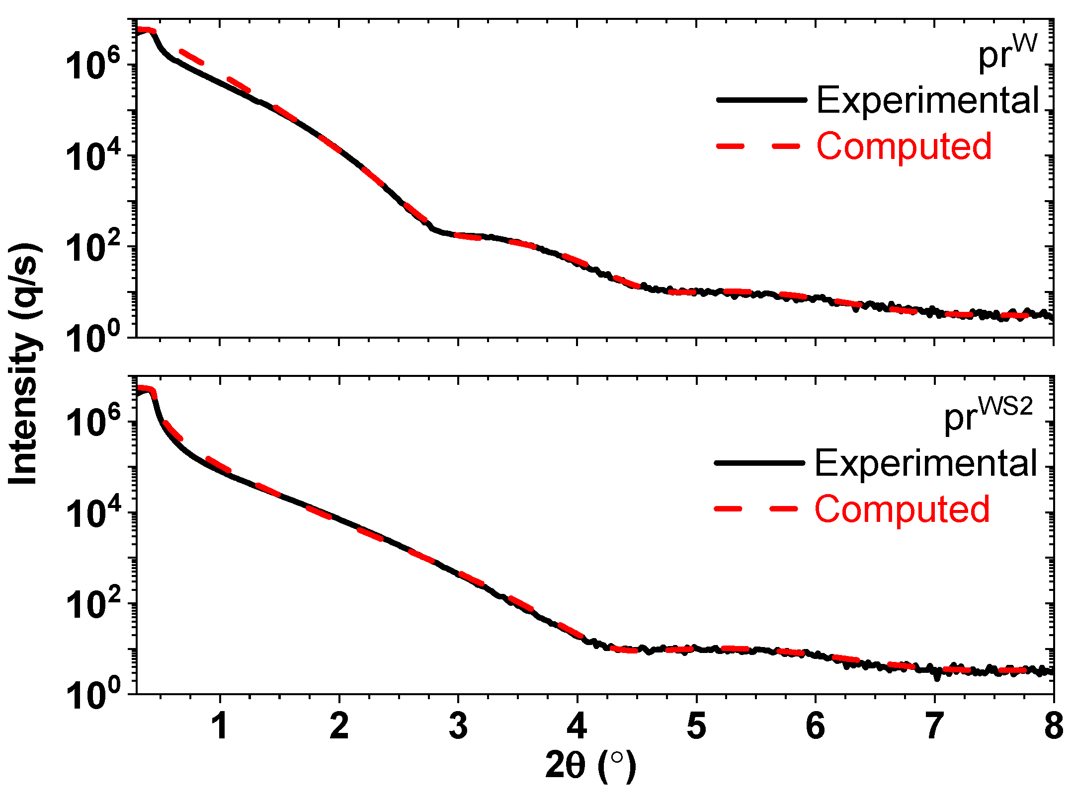
3.1.1. Thickness Determination of prW and prWS2 Precursor Thin Films by XRR

The XRR diagrams for these precursor layers are illustrated in Figure 1. The diagrams show the experimental data (in black) alongside the calculated fits (in red). These fits were generated using the Leptos fitting program, which modeled the films with specific parameters including thickness, electronic density, and surface roughness. For the prW layer, the fitted diagrams estimated a film thickness of 2.9 nm, with a mean mass density of 12.9 g/cm3. This value is notably lower than the density of a bulk W monocrystal, which stands at 19.25 g/cm3. The discrepancy in thickness between the estimated value at deposition and that determined through XRR can be attributed to superficial oxidation of the W film and to its disordered structure. In the case of the prWS2 layer, the estimated thickness was found to be 1.3 nm, with a mean mass density of 7.3 g/cm3. This result is close to the target thickness and to the density of a bulk WS2 monocrystal, which is 7.5 g/cm3.

3.1.2. Structural Determination of prW and prWS2 Precursor Thin Films through XRD

The recorded X-ray diffraction (XRD) patterns for both precursors prW and prWS2 show the absence of distinct diffraction peaks that are typically characteristic of these materials. The absence of the peaks can be primarily attributed to the ultrathin thickness of the films, but also to their amorphous structure since the substrates were not heated during deposition.

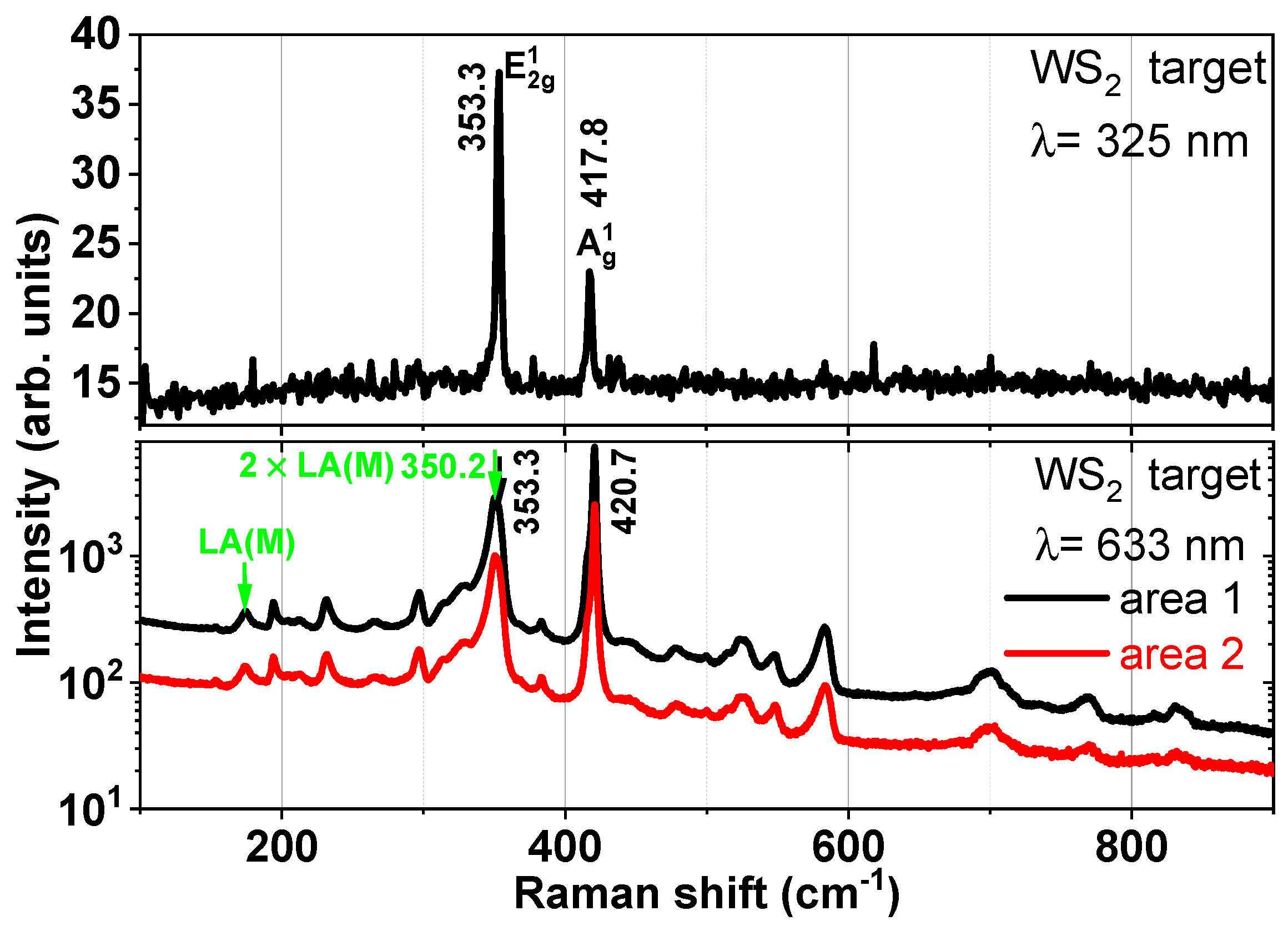
3.1.3. Micro-Raman Spectroscopy Analysis of prW and prWS2 Precursor Thin Films

The first-order Raman active modes in WS2 can be predicted based on its point-group symmetry, making Raman spectroscopy a valuable technique not only for probing the lattice dynamics of but also for highlighting defects within WS2 samples. Unique features in the Raman spectrum, such as double-resonant Raman (DRR) bands associated with phonons within the Brillouin zone activated by defects, are not observed in defect-free samples. DRR processes in WS2 occur between the laser excitation radiation and the direct bandgap at the K point of the Brillouin zone, leading to the creation of excitons and a strong coupling between excitonic states and phononic modes. This coupling amplifies second-order (or even higher order) Raman scattering. The multi-phononic scattering peaks can be categorized into different types, such as the overtone (e.g., 2×), the combination (sum), or the difference between zero-momentum phonons at the Γ point of the Brillouin zone, and similarly the combination of or difference between non-zero momentum phonons, resulting in the creation of two phonons with equal and opposite momentum (e.g., at the M point of the Brillouin zone) [23]. Experimentally, different double-resonant Raman spectra are recorded by varying the excitation energy across the excitonic A and B levels. Excitation with a 532 nm wavelength is in resonance with the excitonic B peak, and 633 nm is in resonance with the excitonic A peak. In a WS2 monolayer, the absence of interlayer coupling and inversion symmetry leads to optical and electronic properties significantly different from those of bulk material [24].
Micro-Raman (m-Raman) spectroscopy was employed to examine the structure of the prW and prWS2 precursor thin films. Utilizing a micron-sized laser spot, the surface of the W target was irradiated in multiple zones to check its uniformity. The m-Raman spectra of prW and prWS2 did not exhibit any Raman peaks, for similar reasons presented in XRD analyses. Therefore, the investigations focused on the W and WS2 sputtering targets in their as-delivered state.
As expected, the W target, due to its cubic-centered lattice containing a single atom per primitive cell, did not exhibit a Raman signal.
In contrast, the Raman spectra for the WS2 target displayed narrow Raman peaks (Figure 2). When using a wavelength of 325 nm, the m-Raman spectrum revealed only first-order Raman modes in the Brillouin zone center, E12g (Γ) at 353.3 cm−1 and A1g (Γ) at 417.8 cm−1 [24,25]. For a 633 nm laser wavelength, the m-Raman spectrum was enriched with additional peaks due to the occurrence of DRR processes. In the vicinity of the E12g (Γ) peak, at around 350 cm−1, a second-order peak of longitudinal acoustic phonons, 2 × LA(M), is prominent [25]. LA(M) is a Raman mode at the Brillouin zone edge—activated by disorder—and it is a collective in-plane movement of the atoms in the lattice, similar to sound waves. It consists of periodic compressions and expansions of the lattice occurring in the direction of propagation. The symbol (M) refers to the specific direction and magnitude of the phonon’s momentum q. In the phonon dispersion (frequency vs. momentum), they appear at the M point of the Brillouin zone. Additional Raman peaks correspond to multi-phononic combinations of these modes.
Berkdemir et al. [24] studied Raman scattering on WS2 flakes, depending on the number of layers and the wavelength of excitation in the visible range (488, 514, and 647 nm). For these three excitation wavelengths, the frequency of the phonon mode A1g(Γ) decreases monotonically with the decrease in the number of layers of a WS2 flake.
The determination of the variation in the E12g(Γ) frequency with the number of layers into a WS2 nanocrystal is difficult to achieve due to its proximity with 2LA(M) peak. This frequency variation in E12g(Γ) is of the order of the error bar when determining the E12g(Γ) and 2LA(M) position by fitting. Frequencies of A1g(Γ), E12g(Γ), 2LA(M), and the intensity ratio I(E12g)/I(A1g), as a function of the number of layers in a WS2 flake, are presented in Table 1 from the work of Berkdemir et al. [24].
In the case of our WS2 target, both the position of the three peaks (A1g(Γ), E12g(Γ), and 2LA(M)) and the ratio I(E12g)/I(A1g) (which is 0.39 and 0.4 for the two tested areas) confirm the bulk state of the WS2 crystallites.

3.1.4. Investigation of the prW and prWS2 Precursor Thin Films by SEM

The scanning electron microscopy (SEM) images reveal a compact and smooth surface for both the prW and prWS2 precursor thin films (images not shown). Utilizing EDX within the microscope setup, the composition of these precursors was approximated as WO0.5 (for prW) and WS0.08 (for prWS2). These findings align with expectations: the prW film exhibits partial oxidation, while the prWS2 film is significantly deficient in sulfur content, and also likely partially oxidized. It is anticipated that these initial discrepancies in the precursor layers’ composition and structure will be effectively improved through a subsequent thermal treatment in a sulfur-rich atmosphere (sulfurization process). The successful correction of these issues is crucial for achieving the desired characteristics and functionality of the final WS2 thin films.

3.2. Sulfurized Thin Films

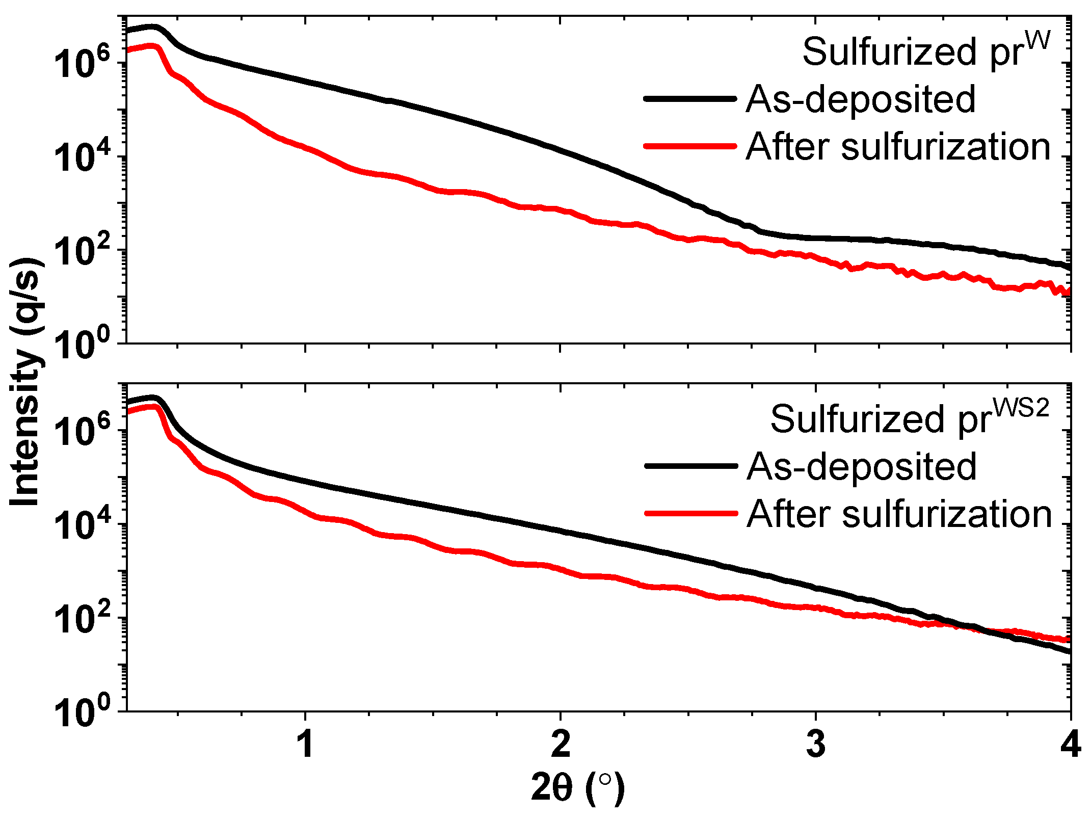
3.2.1. XRR Analysis of Sulfurized prW and prWS2 Thin Films

In exploring the changes after sulfurization, we employed XRR to assess the thickness of the sulfurized prW and prWS2 thin films. The XRR diagrams, depicted in Figure 3, reveal complex details of the sulfurization process’ impact on the films’ thickness. For the sulfurized prW film, the XRR data suggested a bilayer structure with distinct thicknesses of 10 nm and 18 nm. This bilayer formation can be attributed to the differential sulfur incorporation and possibly the presence of intermediate phases or gradients in sulfur concentration. The increased thickness, as compared to the initial precursor, points to significant structural rearrangements and intercalation of sulfur atoms within the tungsten matrix. Similarly, the sulfurized prWS2 film exhibited a dual-layer configuration, with thicknesses measuring 2 nm and 32 nm. This disparity in layer thickness within the same film could indicate areas of varying sulfur content or the formation of distinct phases. The relatively thinner section (2 nm) likely represents a region closer to the ideal WS2 stoichiometry, while the thicker portion (32 nm) may signify regions of excess sulfur or different structural arrangements.

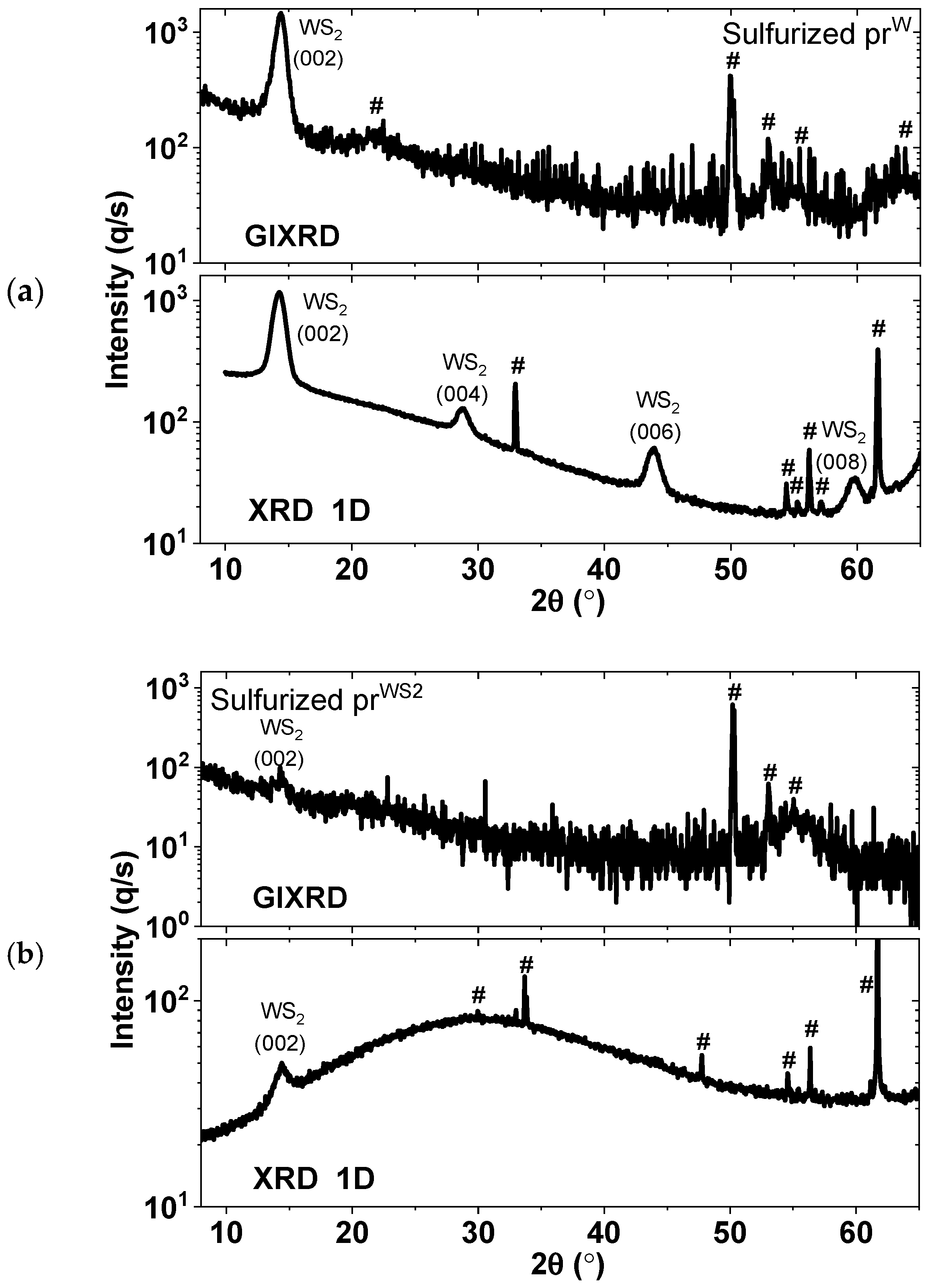
3.2.2. Determining the Structure of Sulfurized prW and prWS2 Thin Films by XRD

The structural analysis of sulfurized prW and prWS2 thin films was conducted using GIXRD (detector in 0D mode) and XRD (Bragg–Brentano geometry with detector in 1D mode). The corresponding diagrams for these films are depicted in Figure 4.
In the sulfurized prW sample, the formation of the hexagonal WS2 phase (h-WS2) is demonstrated (Figure 4a). Moreover, the XRD diagram shows that this phase displayed a preferential orientation of its crystallites, with the (00L) planes parallel to the substrate surface. Furthermore, a deviation from perfect parallelism was inferred from the GIXRD diagram, showing texturing within a range of [−7.2, +7.2]°. The intense maxima of h-WS2 indicate that the prW precursor was not significantly oxidized.
For the sulfurized prWS2 sample, the h-WS2 phase is also demonstrated (Figure 4b). However, due to the extremely thin layer of the sample, it was challenging to ascertain whether there was a preferential orientation of the WS2 crystallites.
In conclusion, the expected result of forming the hexagonal crystalline phase of WS2 with crystallites preferentially oriented with their (00L) planes parallel to the substrate surface was achieved at least for the first precursor.

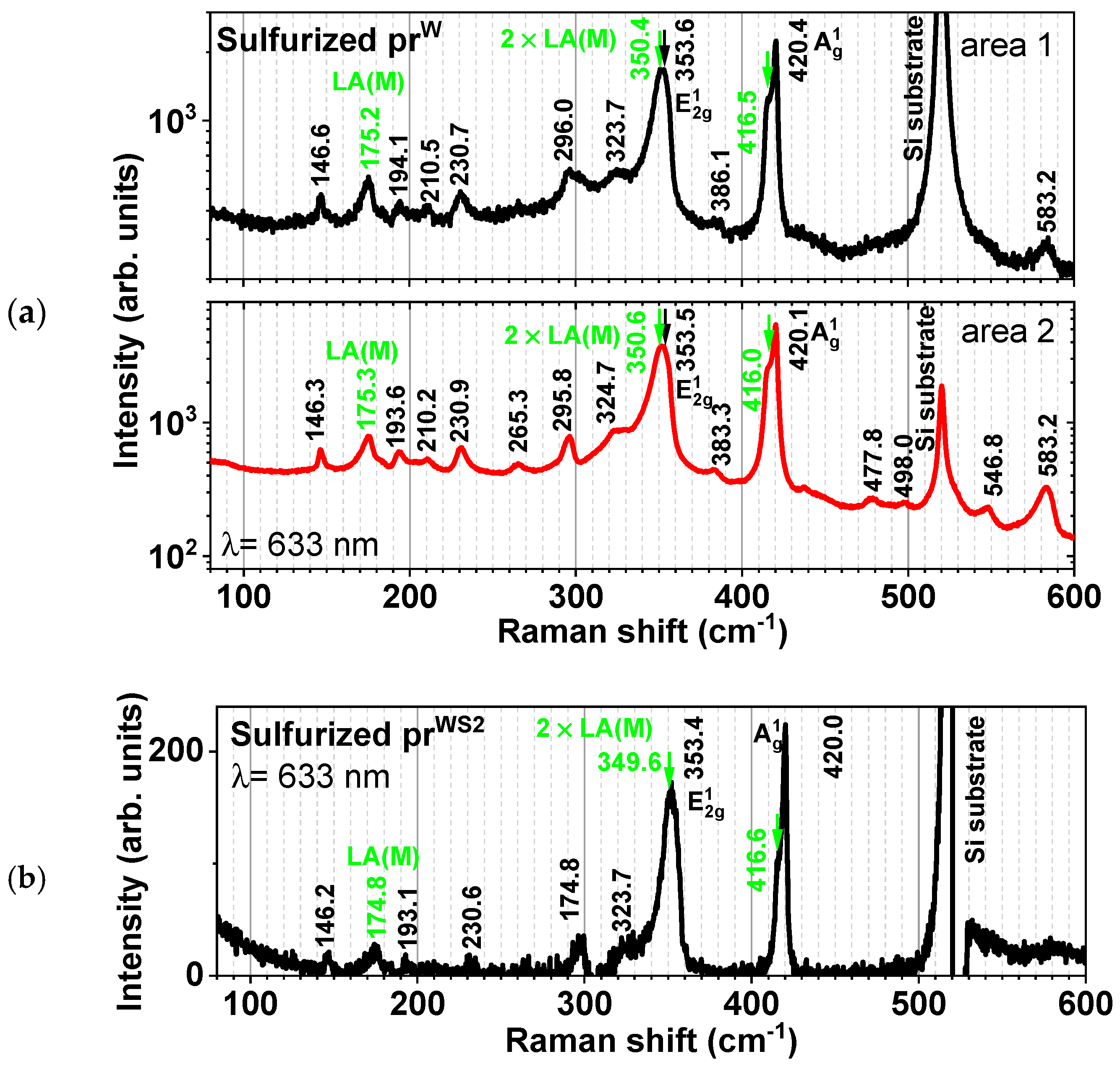
3.2.3. Determining the Structure of Sulfurized prW and prWS2 Thin Films by Micro-Raman Spectroscopy

Upon irradiating the surface of the sulfurized prW and prWS2 samples, in various areas using a micron-sized laser spot, the micro-Raman (m-Raman) spectra were recorded. These measurements, particularly at the excitation radiation wavelength of 633 nm, revealed the presence of double-resonant Raman processes (shown in Figure 5). For a second-order Raman process to meet the requirements for double resonance, the optical excitation energy must match a vertical electronic transition, and the conduction band must contain quasi-isoenergetic electronic states at the difference in momentum corresponding to the phonon’s momentum ±q (or similarly for the valence band in the case of hole–phonon scattering). The momentum dependence of the electronic structure and phonon dispersion must combine to produce a narrow peak in momentum space to yield a narrow double-resonant Raman peak [24]. Analyzing the m-Raman spectra for the prW sample, several observations can be made. Firstly, the sulfurization process resulted in the formation of the hexagonal WS2 crystalline phase, as indicated by the spectrum being almost identical to that of bulk WS2. The intensity variation in the silicon substrate’s peak at 520 cm−1 across different areas of the WS2 layer suggests varying thicknesses, with an intensity ratio higher by 5.3 times in area 1 as compared with area 2. From the frequency value of the A1g peak, we can conclude that WS2 crystallites with more than three layers are formed.
Analyzing the m-Raman spectra of the sulfurized prWS2 sample, we can infer that the formation of the hexagonal WS2 crystalline phase is evident, with peaks aligning with those found in bulk WS2. The silicon substrate’s Raman peak intensity indicates that this sample is thinner than the sulfurized prW sample, with intensity ratios higher by 6.0 to 32.2 times for different analyzed areas. In this case, as well, from the frequency value of the A1g peak, we can conclude that monolayer WS2 was not obtained.

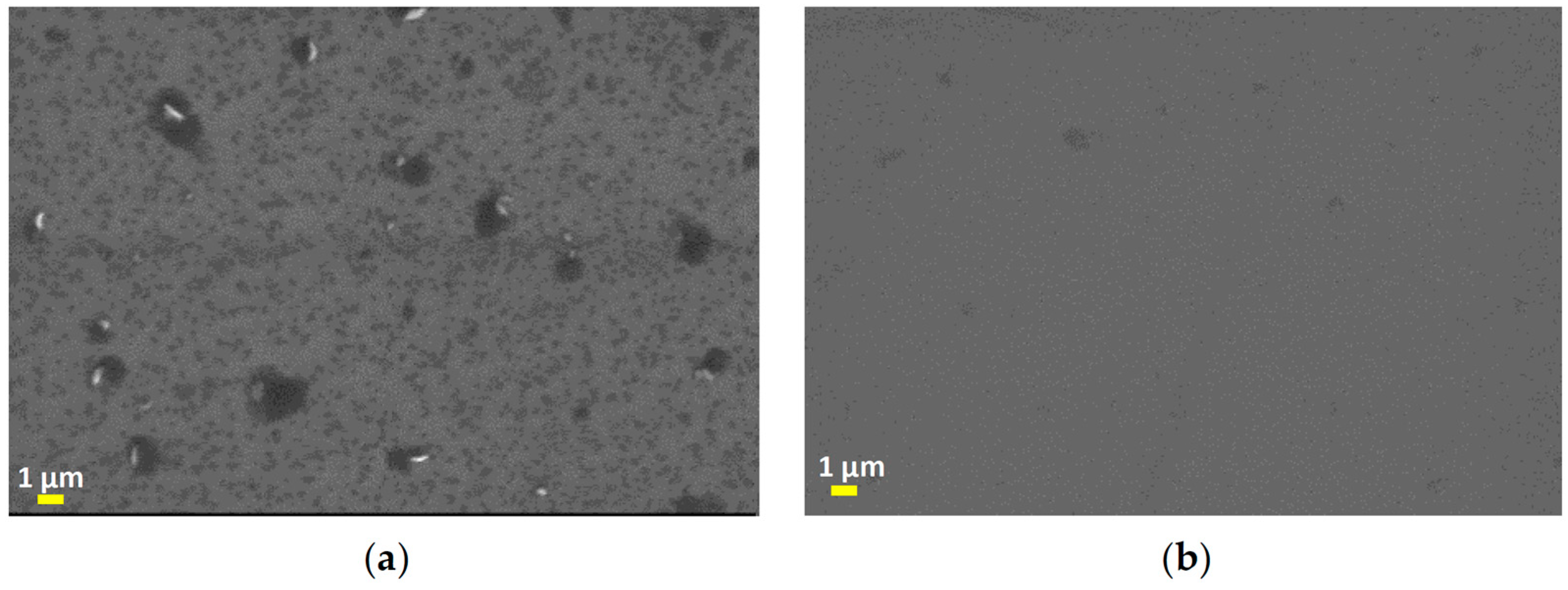
3.2.4. Investigation of Sulfurized prW and prWS2 Thin Films Using SEM and EDX

Scanning electron microscopy provided important insights into the surface morphology and composition of sulfurized prW and prWS2 samples (Figure 6). The SEM images for the sulfurized prW thin film reveal a surface composed of nanometric clusters. These clusters are predominantly planar with an average size of 50 nm, interspersed with fewer vertical clusters averaging 1 μm in size. In contrast, the sulfurized prWS2 thin film shows a smooth uniform surface with few nanometric clusters.
To further elucidate the composition of these sulfurized thin films, energy-dispersive X-ray was employed. The EDX analysis, within the limits of its precision, provided the compositions listed in Table 2. Given that the WS2 phase was confirmed by XRD, it is plausible that a nanometric layer of W (or WSx, where x < 1) that could not be sulfurized remained at the interface with the substrate.

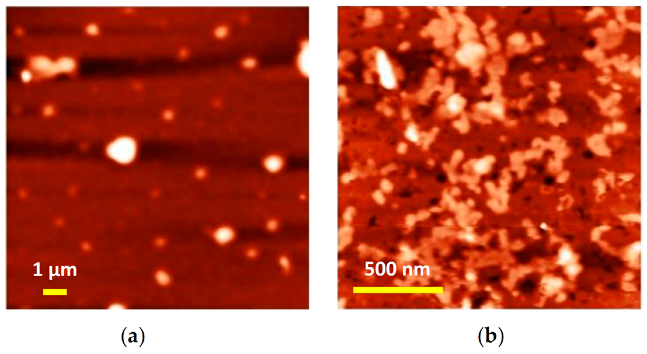
3.2.5. Investigation of Sulfurized prW and prWS2 Thin Layers Using AFM

AFM images reveal that the sulfurized layers comprise non-uniform agglomerations of particles, resulting in a significant increase in surface roughness across the examined areas. The sulfurized prW sample is characterized by an average particle size of approximately 50 nm, with the surface roughness varying between 0.9 nm and 12.3 nm, as shown in Figure 7a. Similarly, the sulfurized prWS2 sample exhibits the same average particle size, but with a surface roughness ranging from 2.2 nm to 4.7 nm, as illustrated in Figure 7b.

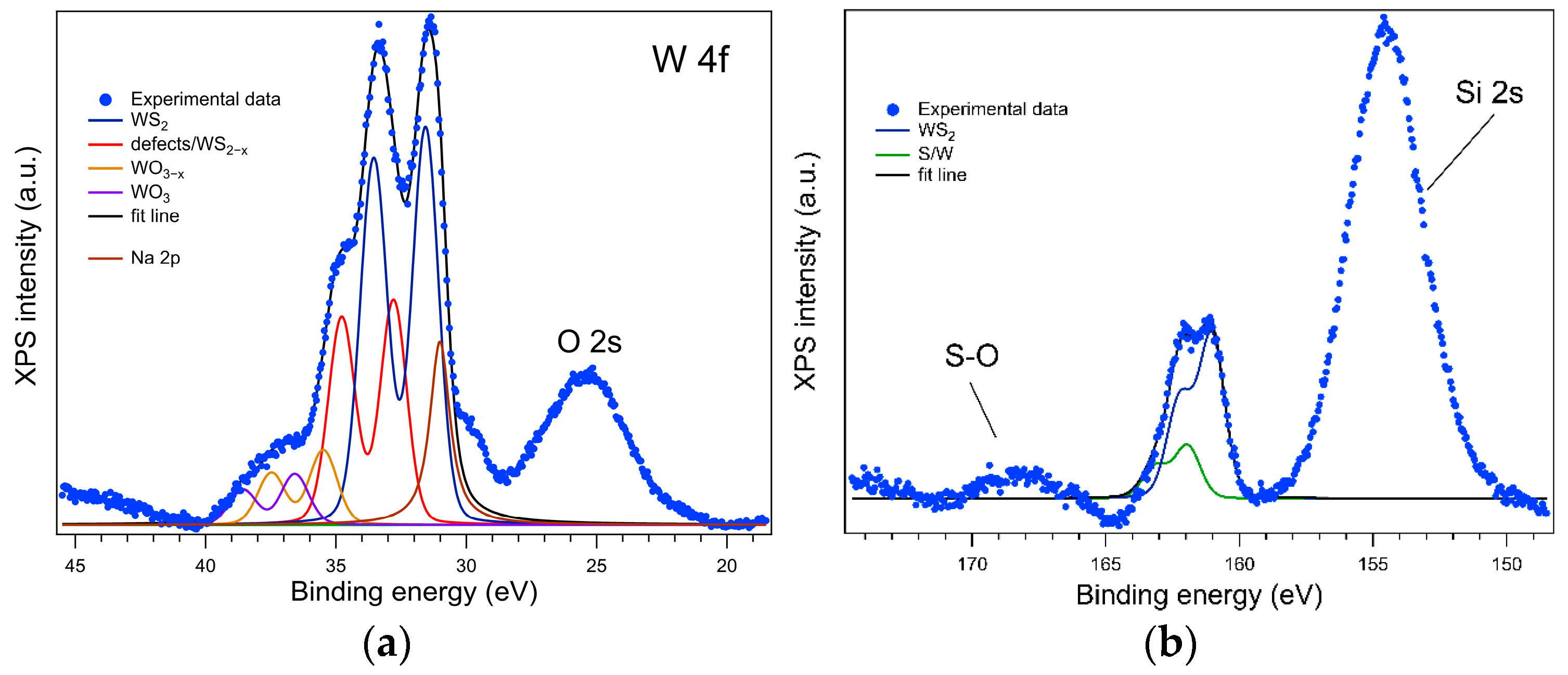
3.2.6. Investigating the Sulfurized prW and prWS2 Thin Films by X-ray Photoelectron Spectroscopy (XPS)

The XPS spectrum for the deep levels of interest of W (4f5/2 and 4f7/2) in the sulfurized prW sample is displayed in Figure 8a. The dominant component in the W 4f spectrum represents WS2, at binding energies of 31.5 eV (4f7/2) and 33.5 eV (4f5/2), accounting for approximately 53% of the integral amplitude. The components at binding energies of 32.8 eV (4f7/2) and 34.8 eV (4f5/2) are associated with W, the undercoordinated WS2, and surface defects. The last two components associated with W-O bonds represent ~16% of the W total. A significant Na 2p contribution overlaps with the W 4f spectrum. This could be due to contamination during sulfurization.
In both the W 4f and S 2p spectra (Figure 8b), the WS2 components are represented with blue lines. The ratio between the integral amplitudes of S/W is 1.9, showing that on the surface the stoichiometry is close to ideal in the compound, while the overall S/W ratio is 1.4. Besides W-S, there is also a contribution from sulfur not bound to W, representing about 20% of the total spectral amplitude. From the S 2p/Si 2s ratio (6.8), after correcting intensities to the photoionization cross-section, it is evident that the substrate coverage is sparse, indicating a non-uniform film.
The XPS spectra for the sulfurized prWS2 film do not exhibit measurable peaks for the deep levels of interest for tungsten and sulfur, and the surface of this sample is dominated by O, Si, and C. In the case of naturally oxidized Si, W-Si interaction is very strong since Si is a very mobile species, so the W atoms tend to migrate deeper in the substrate.

4. Conclusions

This study successfully produced ultrathin films of WS2 from both W and WS2 precursors using a new approach for sulfurization, namely a confined space of a small, closed, graphite box. Better results were obtained through the sulfurization of the W precursor. These thin films were characterized as textured using X-ray diffraction, and the WS2 crystallites grew with their (00L) planes preferentially oriented parallel to the substrate surface. Additionally, a deviation from parallelism in the range of [−7.2, +7.2]° was observed. Micro-Raman spectroscopy provided valuable insights into the crystalline nature of the sulfurized films. For the W precursor, the resulting WS2 phase was identified as being crystallographically similar to bulk WS2, with variable layer thickness across different sample areas. SEM and AFM analyses indicated the presence of nanometric clusters on the surface of the sulfurized films, contributing to increased surface roughness. XPS analysis for the sulfurized W precursor samples revealed that the dominant components in both the W 4f and S 2p spectra are represented by WS2. Overall, this research demonstrates the feasibility of producing ultrathin WS2 layers with potential applications in electronics and optoelectronics. Further investigations into optimizing the sulfurization conditions could lead to improved control over the properties of WS2 layers for specific applications.

Author Contributions

Conceptualization, F.S. and A.V.; methodology, F.S. and A.V.; formal analysis, F.S., I.-D.S., A.-T.B., A.E.B., O.E.K., T.T. and M.Y.Z.; investigation, F.S., I.-D.S., A.-T.B., A.E.B., O.E.K., T.T. and M.Y.Z.; resources, F.S. and A.V.; data curation, F.S.; writing—original draft preparation, F.S. and A.V.; writing—review and editing, F.S., I.-D.S., A.-T.B., A.E.B., O.E.K., T.T., M.Y.Z., C.M. and A.V.; visualization, F.S. and C.M.; supervision, A.V.; project administration, F.S.; funding acquisition, F.S. All authors have read and agreed to the published version of the manuscript.

Funding

This work was funded by the Core Program of the National Institute of Materials Physics, granted by the Romanian Ministry of Research, Innovation and Digitization through the project PC3-PN23080303.

Data Availability Statement

The data presented in this study are available in this article.

Conflicts of Interest

The authors declare no conflicts of interest.

References

  1. Zeng, H.; Wen, Y.; Yin, L.; Cheng, R.; Wang, H.; Liu, C.; He, J. Recent Developments in CVD Growth and Applications of 2D Transition Metal Dichalcogenides. Front. Phys. 2023, 18, 53603. [Google Scholar] [CrossRef]
  2. Buruiana, A.T.; Bocirnea, A.E.; Kuncser, A.C.; Tite, T.; Matei, E.; Mihai, C.; Zawadzka, N.; Olkowska-Pucko, K.; Kipczak, Ł.; Babiński, A.; et al. Layered SnSe Nanoflakes with Anharmonic Phonon Properties and Memristive Characteristics. Appl. Surf. Sci. 2022, 599, 153983. [Google Scholar] [CrossRef]
  3. Buruiana, A.-T.; Sava, F.; Iacob, N.; Matei, E.; Bocirnea, A.E.; Onea, M.; Galca, A.-C.; Mihai, C.; Velea, A.; Kuncser, V. Micrometer Sized Hexagonal Chromium Selenide Flakes for Cryogenic Temperature Sensors. Sensors 2021, 21, 8084. [Google Scholar] [CrossRef] [PubMed]
  4. Mihai, C.; Sava, F.; Galca, A.C.; Velea, A. Low Power Non-Volatile Memory Switching in Monolayer-Rich 2D WS2 and MoS2 Devices. AIP Adv. 2020, 10, 025102. [Google Scholar] [CrossRef]
  5. Novoselov, K.S.; Geim, A.K.; Morozov, S.V.; Jiang, D.; Zhang, Y.; Dubonos, S.V.; Grigorieva, I.V.; Firsov, A.A. Electric Field Effect in Atomically Thin Carbon Films. Science 2004, 306, 666–669. [Google Scholar] [CrossRef] [PubMed]
  6. Zhang, K.; Feng, Y.; Wang, F.; Yang, Z.; Wang, J. Two Dimensional Hexagonal Boron Nitride (2D-hBN): Synthesis, Properties and Applications. J. Mater. Chem. C 2017, 5, 11992–12022. [Google Scholar] [CrossRef]
  7. Sarkar, A.S.; Stratakis, E. Recent Advances in 2D Metal Monochalcogenides. Adv. Sci. 2020, 7, 2001655. [Google Scholar] [CrossRef]
  8. Manzeli, S.; Ovchinnikov, D.; Pasquier, D.; Yazyev, O.V.; Kis, A. 2D Transition Metal Dichalcogenides. Nat. Rev. Mater. 2017, 2, 17033. [Google Scholar] [CrossRef]
  9. Dai, J.; Li, M.; Zeng, X.C. Group IVB Transition Metal Trichalcogenides: A New Class of 2D Layered Materials beyond Graphene. WIREs Comput. Mol. Sci. 2016, 6, 211–222. [Google Scholar] [CrossRef]
  10. Mishra, A.; Mehta, A.; Basu, S.; Shetti, N.P.; Reddy, K.R.; Aminabhavi, T.M. Graphitic Carbon Nitride (g–C3N4)–Based Metal-Free Photocatalysts for Water Splitting: A Review. Carbon 2019, 149, 693–721. [Google Scholar] [CrossRef]
  11. Molina-Sánchez, A.; Wirtz, L. Phonons in Single-Layer and Few-Layer MoS2 and WS2. Phys. Rev. B 2011, 84, 155413. [Google Scholar] [CrossRef]
  12. Roldán, R.; Silva-Guillén, J.A.; López-Sancho, M.P.; Guinea, F.; Cappelluti, E.; Ordejón, P. Electronic Properties of Single-layer and Multilayer Transition Metal Dichalcogenides MX2 (M = Mo, W and X = S, Se). Ann. Phys. 2014, 526, 347–357. [Google Scholar] [CrossRef]
  13. Gusakova, J.; Wang, X.; Shiau, L.L.; Krivosheeva, A.; Shaposhnikov, V.; Borisenko, V.; Gusakov, V.; Tay, B.K. Electronic Properties of Bulk and Monolayer TMDs: Theoretical Study Within DFT Framework (GVJ-2e Method). Phys. Status Solidi (A) 2017, 214, 1700218. [Google Scholar] [CrossRef]
  14. Ballif, C.; Regula, M.; Schmid, P.E.; Remškar, M.; Sanjinés, R.; Lévy, F. Preparation and Characterization of Highly Oriented, Photoconducting WS2 Thin Films. Appl. Phys. A 1996, 62, 543–546. [Google Scholar] [CrossRef]
  15. Li, Y.; Kuang, G.; Jiao, Z.; Yao, L.; Duan, R. Recent Progress on the Mechanical Exfoliation of 2D Transition Metal Dichalcogenides. Mater. Res. Express 2022, 9, 122001. [Google Scholar] [CrossRef]
  16. Voiry, D.; Yamaguchi, H.; Li, J.; Silva, R.; Alves, D.C.B.; Fujita, T.; Chen, M.; Asefa, T.; Shenoy, V.B.; Eda, G.; et al. Enhanced Catalytic Activity in Strained Chemically Exfoliated WS2 Nanosheets for Hydrogen Evolution. Nat. Mater. 2013, 12, 850–855. [Google Scholar] [CrossRef] [PubMed]
  17. Nam, H.; Kim, H.-S.; Han, J.-H.; Kwon, S.J.; Cho, E.S. A Study on the Formation of 2-Dimensional Tungsten Disulfide Thin Films on Sapphire Substrate by Sputtering and High Temperature Rapid Thermal Processing. J. Nanosci. Nanotechnol. 2018, 18, 6257–6264. [Google Scholar] [CrossRef]
  18. Wu, C.-R.; Chang, X.-R.; Chu, T.-W.; Chen, H.-A.; Wu, C.-H.; Lin, S.-Y. Establishment of 2D Crystal Heterostructures by Sulfurization of Sequential Transition Metal Depositions: Preparation, Characterization, and Selective Growth. Nano Lett. 2016, 16, 7093–7097. [Google Scholar] [CrossRef]
  19. Zeng, L.; Tao, L.; Tang, C.; Zhou, B.; Long, H.; Chai, Y.; Lau, S.P.; Tsang, Y.H. High-Responsivity UV-Vis Photodetector Based on Transferable WS2 Film Deposited by Magnetron Sputtering. Sci. Rep. 2016, 6, 20343. [Google Scholar] [CrossRef]
  20. Wu, C.-R.; Chang, X.-R.; Wu, C.-H.; Lin, S.-Y. The Growth Mechanism of Transition Metal Dichalcogenides by Using Sulfurization of Pre-Deposited Transition Metals and the 2D Crystal Hetero-Structure Establishment. Sci. Rep. 2017, 7, 42146. [Google Scholar] [CrossRef]
  21. Jung, Y.; Shen, J.; Liu, Y.; Woods, J.M.; Sun, Y.; Cha, J.J. Metal Seed Layer Thickness-Induced Transition From Vertical to Horizontal Growth of MoS2 and WS2. Nano Lett. 2014, 14, 6842–6849. [Google Scholar] [CrossRef] [PubMed]
  22. Mihai, C.; Sava, F.; Simandan, I.D.; Galca, A.C.; Burducea, I.; Becherescu, N.; Velea, A. Structural and Optical Properties of Amorphous Si–Ge–Te Thin Films Prepared by Combinatorial Sputtering. Sci. Rep. 2021, 11, 11755. [Google Scholar] [CrossRef] [PubMed]
  23. Zhao, W.; Ghorannevis, Z.; Amara, K.K.; Pang, J.R.; Toh, M.; Zhang, X.; Kloc, C.; Tan, P.H.; Eda, G. Lattice Dynamics in Mono- and Few-Layer Sheets of WS2 and WSe2. Nanoscale 2013, 5, 9677. [Google Scholar] [CrossRef] [PubMed]
  24. Berkdemir, A.; Gutiérrez, H.R.; Botello-Méndez, A.R.; Perea-López, N.; Elías, A.L.; Chia, C.-I.; Wang, B.; Crespi, V.H.; López-Urías, F.; Charlier, J.-C.; et al. Identification of Individual and Few Layers of WS2 Using Raman Spectroscopy. Sci. Rep. 2013, 3, 1755. [Google Scholar] [CrossRef]
  25. Sourisseau, C.; Cruege, F.; Fouassier, M.; Alba, M. Second-Order Raman Effects, Inelastic Neutron Scattering and Lattice Dynamics in 2H-WS2. Chem. Phys. 1991, 150, 281–293. [Google Scholar] [CrossRef]
Figure 1. XRR diagrams of the prW and prWS2 precursor thin films. The experimental XRR patterns (in black) for both prW and prWS2 thin films, overlapping with their respective fitted diagrams (in red). The fitted curves are derived based on a specific model of each thin film, accounting for thickness, electronic density, and surface roughness.
Surfaces 07 00008 g001
Figure 2. Micro-Raman spectra for two excitation radiation wavelengths (325 nm and 633 nm) of the WS2 sputtering target. Different areas of the target were examined to check the uniformity. Some of the double-resonant Raman bands, the LA(M) peaks, are highlighted in green.
Surfaces 07 00008 g002
Figure 3. XRR diagrams of sulfurized prW and prWS2 thin films. The XRR diagrams of the as-deposited prW and prWS2 films (in black) are added for comparison.
Surfaces 07 00008 g003
Figure 4. GXRD (detector in 0D mode) and XRD (detector in 1D mode) diagrams of sulfurized thin films: (a) prW and (b) prWS2. Peaks marked with ‘#’ represent diffraction maxima of Si substrate.
Surfaces 07 00008 g004
Figure 5. Micro-Raman spectra at the excitation radiation wavelength of 633 nm for sulfurized (a) prW and (b) prWS2 thin films. Some of the double-resonant Raman bands are highlighted in green.
Surfaces 07 00008 g005
Figure 6. SEM images of the surfaces of (a) prW and (b) prWS2 sulfurized samples.
Surfaces 07 00008 g006
Figure 7. AFM images of the surface of sulfurized samples: (a) prW and (b) prWS2.
Surfaces 07 00008 g007
Figure 8. XPS spectrum for the deep levels of (a) W (4f5/2 and 4f7/2) and (b) sulfur (2p1/2 and 2p3/2) in the prW sulfurized thin films.
Surfaces 07 00008 g008
Table 1. Frequencies and intensity ratios of Raman active modes A1g(Γ), E12g(Γ), and 2LA(M) as a function of the number of layers in WS2 thin films [24].
λ (nm)PhononsMonolayer (cm−1)Bilayer (cm−1)Trilayer (cm−1)Bulk (cm−1)
647A1g(Γ)417.2418.7419.2420.5
E12g(Γ)355.3354.2354354.7
2LA(M)350.4349.5349.5351.1
I(E12g)/I(A1g)0.50.80.80.4
Table 2. The composition of the sulfurized thin films determined by EDX.
SampleComposition
Sulfurized prWW76S24
Sulfurized prWS2W93S7
Disclaimer/Publisher’s Note: The statements, opinions and data contained in all publications are solely those of the individual author(s) and contributor(s) and not of MDPI and/or the editor(s). MDPI and/or the editor(s) disclaim responsibility for any injury to people or property resulting from any ideas, methods, instructions or products referred to in the content.

