

Abstract
Using numerical integration of the Boltzmann transport equation, depth distributions of recoil-implanted Ga and N atoms in Mg-implanted GaN are studied. Mg implantation into GaN is found to produce significant nonuniform stoichiometric distribution as a consequence of the recoil process, as compared to other III–V materials of GaP, GaAs and GaSb. Our calculation also indicates that the stoichiometric imbalance introduced by Mg implantation in GaN is insensitive to the changes in the implanted ion energy and the atom density of the target material. These results suggest that stoichiometric imbalance may be one of the principal reasons why the electrical activation of implanted Mg acceptors in GaN is rather difficult as compared to that in other III–V semiconductors.
Export citation and abstract BibTeX RIS

Content from this work may be used under the terms of the Creative Commons Attribution 4.0 license. Any further distribution of this work must maintain attribution to the author(s) and the title of the work, journal citation and DOI.
1. Introduction
GaN-based transistors are expected as essential devices for low-loss and high-voltage power applications. 1–5) Above all, GaN-based vertical transistors are receiving significant attention as high-voltage and high-current-density power switching devices. 6–17) Since only layered structures are prepared by standard epitaxial techniques, local junction structures have to be formed via dry etching and/or selective regrowth technique, leading to non-planar device structures with associated damage issues. In order to avoid these difficulties, magnesium (Mg) ion implantation into GaN is now extensively studied to make p-type channel and low-resistivity p-type contact layers. 18–27) It was verified by optical characterization that acceptor centers were formed after thermal annealing of Mg-implanted GaN. 18–20) However, with the exception of recent experimental results using ultra-high-pressure annealing, 24–27) only partial electrical activation of Mg has been observed by using conventional activation annealing procedures. 22)
Ion implantation is known as a reproducible and high-yield doping technique. Using this technology, complicated planar semiconductor structures can be prepared with well-defined lateral controllability for both p-type and n-type conductivities. This is due to its potential capability of selective-area processing with a precise doping concentration. Using a well-known analytical statistical theory of Lindhard, Scharff and Schiott, one can calculate the ion range profile by using tabulated values of the average projected range and its standard deviation. 28–33) Contrary to the ion implantation into Si, it was predicted that ion implantation into compound semiconductors induces local stoichiometry disturbance in addition to the generation of the damaged lattice. Such additional difficulties might apply to GaN and result in unsatisfactory electrical activation of Mg acceptors implanted into GaN.
Christel and Gibbons proposed an algorithm to calculate momentum distributions of moving atoms in various materials by numerically solving the Boltzmann transport equation. 34,35) In this method, the kinetic energy and the direction of moving atoms, including both primary ions and recoil-implanted atoms, are numerically traced with respect to the depth from the semiconductor surface, thus enabling the calculation of displaced atoms distribution in the target material. In this way, one can calculate in-depth information on local stoichiometry imbalance after ion implantation into compound semiconductors. Although various examples of such calculations on local stoichiometry disturbance have been reported, 35) there have been no calculations reported on ion-implanted GaN.
In this work, this approach was applied to the calculation of momentum distributions of recoil-implanted Ga and N atoms in Mg-implanted GaN. As a result, it was found that the effect of implantation-induced stoichiometry disturbance was of appreciable significance in GaN, as compared to that induced in other III–V compound semiconductors. Possible mechanisms for the serious stoichiometry imbalance in GaN are discussed.
2. Calculation procedure
Following the approach proposed by Christel and Gibbons, 34,35) the time-integrated momentum distribution functions of moving atoms, including primary and recoil-implanted atoms, were calculated stepwise as a function of depth z normal to the target surface. The distribution function of each type of particle moving in the material is represented by the Boltzmann transport equation:
Here, F( p ) denotes the momentum distribution function of atoms with momentum p , dσ is the scattering cross section, and N is the number density of the target atoms. In our calculation, momentum p was represented by the kinetic energy E of the atom and the angle θ of its moving direction with respect to the target surface normal direction. Q( p ) is the generation term, corresponding to the distribution of recoil atoms created from rest. For simplicity, the target material was assumed amorphous, and thus no channeling effects were incorporated. With initial conditions at z = 0, the transport equation was numerically integrated in z, thus determining the momentum distributions at all depths. The procedure to calculate the depth dependent distribution function of each atom is schematically illustrated in Fig. 1.

Fig. 1. (Color online) Illustration of momentum distributions for Mg, Ga, and N atoms at depth z.
Download figure:
Standard image High-resolution imageNuclear collisions (elastic) and electronic stopping process (inelastic) were considered as two independent scattering mechanisms. The elastic nuclear event was assumed as classical two-body mechanics, in which angular deflections of both incident and recoil atoms occurred with energy transfer between those atoms. Thus, only nuclear events generated recoil atoms. As for the form of the elastic nuclear cross section, the analytical expression developed by Christel and Gibbons was adopted. 34,35) The electronic stopping was introduced as a drag force causing only energy reduction with no angular deflections of the moving atoms. 28)
Each particle was assumed stopped when its kinetic energy was reduced to less than some critical value (Es) or when the particle was directed toward the semiconductor surface. In this way, the range distributions of both primary and recoil particles were determined at each depth in the target material.
3. Results
In this section, the calculated results for the local stoichiometric disturbance in Mg-implanted GaN are presented.
Figure 2 shows the concentrations of net vacancies and net displaced atoms of Ga and N as a function of the depth, together with the implanted Mg atom profile (220 keV, 1015 cm−2). Open squares and triangles indicate a net vacancy distribution, while closed squares and triangles indicate a net displaced atom distribution. The latter distribution is obtained by subtracting the vacancy distribution from the calculated recoil atom distribution. The average projected range of the Mg profile is 0.21 μm when it is defined as the depth of the peak Mg concentration. This value is slightly smaller than the value of 0.26 μm calculated by SRIM, 36) probably due to different collision parameters employed. Note that a rather flat profile of net vacancies (Ga and N) is generated in the shallow region, while recoil-implanted atoms are accumulated in the deeper region as interstitial atoms. Careful observation reveals that N atoms have much larger concentrations in both profiles of net vacancies and displaced atoms. This is because, in principle, the lighter atoms have greater ranges than the heavier atoms of the same energy. This trend and mechanism have been discussed by Christel and Gibbons, 35) in which they concluded that the effect of stoichiometric imbalance was greatest when the mass ratio of the constituent elements of the compound was high. As a measure of estimating such stoichiometric imbalance between group III and group V lattice atoms, we define the peak density ratio (PDR) as the peak density of net displaced N atoms divided by that of net displaced Ga atoms. From Fig. 2, we see that PDR reaches as high as 2.6 in GaN. The higher PDR is well correlated with the formation of higher-density profile of N vacancies near the surface region. Considering that implanted Mg should occupy Ga sites as acceptors, the formation of higher-density N vacancies in the shallow region (less than 0.15 μm) is not beneficial for achieving increased electrical activation of acceptors by Mg implantation into GaN.
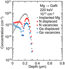
Fig. 2. (Color online) Stoichiometric distribution in GaN implanted with 220 keV Mg.
Download figure:
Standard image High-resolution imageFigure 3 shows the concentrations of net vacancies and net displaced atoms in GaP implanted with Mg (220 keV, 1015 cm−2) as a function of the depth from the surface. Since the atomic number and mass of P is still much smaller than those of Ga, the general trend of recoil-implanted atom distribution in GaP is similar to the distribution in GaN, resulting in a high PDR value of 1.8.

Fig. 3. (Color online) Stoichiometric distribution in GaP implanted with 220 keV Mg.
Download figure:
Standard image High-resolution imageFigure 4 shows the calculated distributions of vacancies and displaced atoms in GaAs implanted with Mg (220 keV, 1015 cm−2). Since the atomic number and mass of Ga are very similar to those of As in GaAs, the effect of stoichiometric imbalance is almost negligible in both shallower (with high density of vacancies) and deeper (with high density of displaced atoms) regions. Therefore, the calculated PDR is nearly 1.0 for GaAs. Although the effect of local stoichiometric disturbance is minimal in GaAs, the displaced lattice atoms in the deeper region generate a significant amount of interstitial defects by occupying the normally unoccupied lattice sites. It was reported that the hole concentration profile in 80 keV Mg-implanted GaAs, which was rapid-thermally annealed at 900 °C, exhibited a characteristic double-hump profile, in which the locally reduced hole concentration region well corresponded to the peak position of the generated interstitial defects. 37,38)
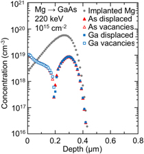
Fig. 4. (Color online) Stoichiometric distribution in GaAs implanted with 220 keV Mg.
Download figure:
Standard image High-resolution imageFigure 5 shows the calculated distributions of vacancies and displaced atoms in GaSb implanted with Mg (220 keV, 1015 cm−2). In contrast to the profiles of the former 3 materials, Mg implantation into GaSb generated a lower concentration profile of net Sb vacancies and net displaced Sb atoms than those for the group III atom of Ga. This is because the atomic number and mass of Sb are larger than those of Ga. Reflecting the smaller concentration of net displaced Sb atoms, the PDR is calculated to be 0.7, indicating Ga-rich stoichiometric imbalance becomes significant in GaSb.

Fig. 5. (Color online) Stoichiometric distribution in GaSb implanted with 220 keV Mg.
Download figure:
Standard image High-resolution imageIn Fig. 6, the calculated values of PDR are plotted as a function of the atomic number of group V atoms in III–V semiconductors (GaN, GaP, GaAs, and GaSb), which are implanted with 220 keV Mg. The results show that the magnitude of PDR becomes highest in GaN and then decreases with the increase in the atomic number of constituent group V element. Similar calculations were also performed for these III–V semiconductors while varying the primary Mg ion energy from 100 to 330 keV. Nevertheless, the calculated trend of PDR was essentially the same as that in Fig. 6 with only a small deviation of 3%. These results imply that Mg implantation into GaN is most complicated in view of defect formation associated with local stoichiometric disturbance. This may be one of the reasons why the electrical activation of Mg acceptors is rather difficult by post-implantation annealing.

Fig. 6. (Color online) Peak density ratio (PDR) as a function of group V atomic number for GaN, GaP, GaAs, and GaSb.
Download figure:
Standard image High-resolution image4. Discussion
In the calculation of PDR, the atom density was precisely chosen for GaN, GaP, GaAs and GaSb as 8.8 × 10²², 4.9 × 10²², 4.6 × 10²², 3.5 × 1022 cm−3, respectively. From Fig. 6, we see that the atom density gradually decreases with increasing the atomic number. To see if there is a correlation between the decrease in PDR and the atom density, PDR was again calculated by assuming that each atom density was fixed at 8.8 × 1022 cm−3 (corresponding to the atom density of GaN). Nevertheless, PDR was found to be almost unchanged by varying the atom density with only a slight deviation within 4%. From these calculations, it was confirmed that the magnitude of PDR was primarily determined by the atomic number of group V atoms, and not by the atom density of the target material.
To further investigate the effect of group V atoms on PDR, a similar calculation was performed while assuming a hypothetical material of GaX, in which the atomic number of X (corresponding to group V atom) was virtually varied between 2 and 20. Figure 7 plots the calculated PDR for such hypothetical GaX materials, together with the results for the real materials of GaN, GaP, GaAs and GaSb. In all calculations, the atom density of each material was fixed at 8.8 × 1022 cm−3 to avoid any effects coming from the atom density. Contrary to the initial expectation, PDR was found to first saturate and then decrease with decreasing the atomic number of X. A maximum PDR of 2.65 was calculated at a virtual atomic number of 6. These results demonstrate that GaN is indeed the III–V material where essentially the most significant stoichiometric imbalance is generated by ion implantation.
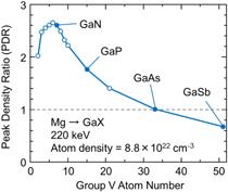
Fig. 7. (Color online) Peak density ratio (PDR) as a function of group V atomic number for hypothetical semiconductor material of GaX.
Download figure:
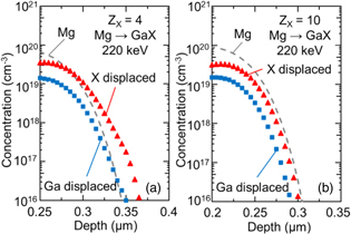
Standard image High-resolution imageFigures 8(a) and 8(b) show the recoil-displaced atom concentrations produced by 220 keV Mg implantation as a function of the depth, calculated for a hypothetical semiconductor material of GaX, in which a group V atomic number was assumed to be 4 and 10, respectively. The profile of the implanted Mg was also plotted as a reference. When the atomic number of X is 4 (ZX = 4), the profile of displaced X atoms shifts to a deeper range, which is beyond the primary Mg ion range. A similar calculation was reported in 400 keV Se implanted InP, in which the density of net displaced P atoms exceeded that of the primary Se ions in the deeper range. 35) Meanwhile, when the atomic number of X is increased to 10 (ZX = 10), the displaced X atoms are within the Mg profile. This is because the lattice atoms with a smaller atomic number are easier to be knocked into a deeper region, thus making a rather broadened atom profile with a reduced peak density. This is the plausible reason why PDR presented a saturated trend at an atomic number of around 7 and then started to decrease again when the atomic number of X was further decreased to less than 7, as shown in Fig. 7.
Fig. 8. (Color online) Recoil-displaced atom distribution in GaX for (a) ZX = 4 and (b) ZX = 10.
Download figure:
Standard image High-resolution image
Since the electrical activation of implanted ions is well-known to be greatly affected by the way of post-implantation annealing, it is not possible to make a reasonable prediction of the activation efficiency through our simulation. However, we believe that PDR would be a good quantitative measure for such a purpose because the knowledge of lattice disorder including stoichiometric disturbances by ion implantation is of primary importance to predict the difficulty in electrical activation.
5. Conclusions
We have calculated local stoichiometric imbalances in GaN implanted with Mg by using a stepwise numerical approach, developed by Christel and Gibbons, for integrating the Boltzmann transport equation. In the calculation, elastic nuclear stopping and inelastic electronic stopping were considered as two independent scattering mechanisms. The results indicated that the effect of local stoichiometric disturbance by implanting Mg ions became most significant in GaN, as compared to other well-known III–V materials, such as GaP, GaAs, and GaSb. As a measure of stoichiometric imbalance introduced by ion implantation, we defined the PDR as a ratio between peak densities of net displaced N and Ga atoms. It was found that PDR increased with the decrease in the atomic number of group V atom and reached 2.6 in GaN. The trend was insensitive to the changes in the implanted ion energy and the atom density of the target material. These results suggested that the significant stoichiometric imbalance induced in GaN may be the possible reason why achieving high electrical p-type activation in Mg-implanted GaN is rather difficult as compared to the cases for other III–V semiconductors.
Acknowledgments
This work was partially supported by Grant-in-Aid for Scientific Research (A) (No.19H00761) from JSPS.