
Abstract
We recently invented a method called the flux-film-coated technique for purifying a GaN wafer with low dislocation density grown from point-seed crystals. In this study, we investigated the mechanism behind the reduction of dislocation density in the GaN wafer by evaluating the three-dimensional behavior of dislocations using multiphoton-excitation photoluminescence images. We made the surprising discovery that dislocations more than 50 μm away disappeared by annihilating each other as growth proceeded, and this is one of the mechanisms underlying the dislocation density reduction. The moving distance of dislocations before annihilation is uncommon and a unique phenomenon in the Na-flux method.
Export citation and abstract BibTeX RIS

Content from this work may be used under the terms of the Creative Commons Attribution 4.0 license. Any further distribution of this work must maintain attribution to the author(s) and the title of the work, journal citation and DOI.
GaN substrates are widely anticipated to enable high-performance optoelectronic and electronic power devices.1–7) To make widespread use of such GaN devices possible, however, the production cost of GaN substrates must be reduced. Moreover, the threading dislocation density (TDD) in those substrates should be further reduced. To achieve these goals and promote mass production, procedures are needed which allow faster growth of thicker and larger-diameter bulk GaN crystals with low TDD that can be sliced. In order to achieve such ideal GaN crystals, various growth techniques—such as the hydride vapor phase epitaxy (HVPE) method, the ammonothermal method, or a combination of both—have been studied by many researchers.8–13) We also attempted HVPE homoepitaxial thick growth on a seed GaN wafer produced with a multi-point-seed (MPS) technique by the Na-flux method.14) Large-diameter (>2'') GaN wafers with low TDD on the order of 103–105 cm−2 could be obtained after the coalescence of crystals grown from individual small seeds.15) However, the lattice constant of the seed wafer expands due to the high concentration of oxygen impurities in {10 1}-facet planes, which always appear during growth on point seeds. As a result of the lattice mismatch, a large number of cracks and threading dislocations (TDs) are generated in the HVPE GaN layer.
Therefore, we recently invented an advanced point-seed technique based on our the flux-film-coated (FFC) technique.16,17) In the advanced point-seed technique, a thin layer of Ga–Na melt is maintained in a V-shaped valley between {10 1} the facets of GaN crystals by pulling up the wafer from the melt in a crucible, which permits growth only along the lateral direction. Consequently, {10
 1} facets were suppressed and 2 inch GaN wafers fully composed of c-planes were successfully realized with low oxygen concentration. This new technique enabled thick HVPE growth,18) and opened up the possibility of obtaining bulk GaN wafers.
On the other hand, the mechanisms by which the TDD is reduced in the point-seed technique have not been sufficiently investigated, although it has been reported that low TDD GaN can be grown from point seeds. In studies using a conventional method of selective area growth such as the epitaxial lateral growth (ELO) technique, it has been reported that TDs with high density over 106 cm−2 exist at the coalescence boundary of grains.19,20) Shida et al. recently reported that in the case of the FFC technique, TDs were estimated to gather around the coalescence boundary, as well as from nanobeam X-ray diffraction measurement.21) Nevertheless, the TDD values at the surface were not as high as in other growth techniques, and the mechanism of TD reduction was unclear. In this study, we therefore carefully evaluated the three-dimensional (3D) behavior of TDs from the inside to the surface around the coalescence region by directly capturing TDs using multiphoton excitation photoluminescence (MPPL).
An MPS-GaN substrate was produced by the selective area growth of 5 μm thick c-plane GaN crystals in a circular shape with 250 μm diameter, on a 4 inch diameter (0001) sapphire substrate by the metal organic vapor phase epitaxy technique. Those GaN crystals "point seeds" were arranged at regular intervals in a hexagon area with a diagonal of 93 mm. As starting materials, metallic Ga (purity: 6N), metallic Na (purity: 4N), and granular graphite (purity: 4N) were added to a ceramic crucible in an Ar-filled glovebox. Granular graphite was added to suppress polycrystal generation on the crucible wall, and to improve the growth rate and yield.22,23) The growth was carried out for 236 h at 860 °C–880 °C, 3.4 MPa through the FFC process. More details regarding the growth conditions were provided in a previous paper.17)
The TDD and behavior of individual dislocations in the wafers were measured by MPPL (Nikon; A1RMP), in which an in-plane image at each focal depth was obtained by varying the focal depth.24) Structural properties in large areas were evaluated from the FWHM values of the GaN 0002 X-ray rocking curves (XRCs) (Rigaku, SmartLab-ES; Cu−Kα; 40 kV; 30 mA). The radius of the lattice curvature was also estimated by a shift in the peak top angle of the GaN 0002 ω-scan XRC profiles with the incident X-ray directions parallel to the a-direction of the GaN. Bright field X-ray topography under multiple-diffraction conditions was performed at the BL24XU beamline of SPring-8,25,26) to determine the Burgers vectors of the TDs in the grown crystal.
A crack-free GaN crystal was successfully obtained after growth, as shown in the photo of the as-grown crystal in Fig. 1(a). The sapphire in the MPS-GaN substrate naturally separated out without cracking during the cooling process. The grown crystal had a regular hexagonal shape with a diagonal of 96 mm. The grown crystal was gray in color due to the facet growth region, which always appears black because of oxygen impurities in the initial growth stage.14) Thus, after the backside region was ground, and both the surface and backside underwent chemical mechanical polishing (CMP), the wafer showed high transparency, as shown in Fig. 1(b).
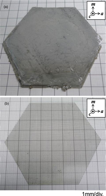
Fig. 1. Photographic images of: (a) the as-grown GaN crystal fabricated with the FFC technique; and (b) the GaN wafer after CMP processing on both the surface and backside.
Download figure:
Standard image High-resolution imageFigure 2(a) shows on-axis GaN 0002 ω-XRCs when the incident X-ray beam is parallel to the a-direction (a//). Taking 9 points for 10 mm steps, lines of measurements were performed. The X-ray spot size was over 10.0 × 3.4 mm2, as calculated from the Bragg angle and divergence slit width. All XRCs exhibited a single peak. FWHM values were as narrow as 30–40 arcsec, indicating that the crystallinity was homogeneous across the entire sample surface. The GaN wafer was slightly bowed concave up, with a radius of curvature of approximately 30 m. The TDD around the surface was evaluated by dark-spot density in a 210 μm square area of MPPL images with a mapping of 3 × 3 points with the scheme showing the location of point seeds and coalescence boundaries [Fig. 2(b)]. The lowest TDD was 9.0 × 103 cm−2; the highest was 2.3 × 105 cm−2; and the average TDD was 5.1 × 104 cm−2. The evaluation was also performed in other regions, where the TDD values were almost the same. Moreover, these values were almost the same as those for the crystal grown on a 3 inch MPS substrate obtained in a previous study,17) so we expect that the FFC technique will easily allow the enlargement of GaN wafers.
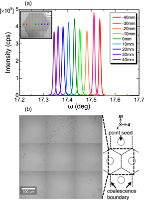
Fig. 2. (Color online) (a) On-axis GaN 0002 ω-XRCs when the incident X-ray beam is parallel to the a-direction (a//). Taking 9 points for 10 mm steps, lines of measurements were performed along the incident X-ray direction. (b) A 210 μm square area of MPPL images with a mapping of 3 × 3 points, i.e. a 630 μm square, with a schematic showing the location of point seeds and coalescence boundaries.
Download figure:
Standard image High-resolution imageSubsequently, the mechanisms of the reduction of the TDD were carefully investigated by varying the focal depth of the MPPL image. We focused on the area surrounded by three GaN crystals grown from their respective point seeds, as illustrated in Fig. 3(a), where a comparatively high TDD area on the order of 105 cm−2 existed at the surface. MPPL images were taken at two depths: above and below the depth at which crystals completely coalesced and the surface was completely composed of the c-plane, as shown in a schematic drawing of the cross-section in Fig. 3(b). The observation was performed in two different regions; Figs. 3(c) and 3(d) show 320 μm square MPPL images at the shallow level (surface side) of the two regions; and Figs. 3(e) and 3(f) show the regions at the deeper level. The TDD in Fig. 3(c) was on the order of 104 cm−2, while that in Fig. 3(d) was too high to determine (probably more than 106 cm−2). In addition, numerous basal plane dislocations (BPDs) were generated, which can be observed as dark winding lines in the MPPL images shown in Figs. 3(d) and 3(f). A few BPDs were also evident in Figs. 3(c) and 3(e). Thus, the number of dislocations generated at the coalescence boundary was found to vary by region. The reason for the variation is unclear, but it appeared to be related to the shape of the coalescence boundaries. The shape seen in Fig. 3(e) was closer to threefold symmetry (i.e. crystals coalesced within a uniform shape) compared to that in Fig. 3(f). Thus, the number of dislocations may depend on the uniformity of crystals grown from each point-seed.

Fig. 3. (Color online) Schematic drawings of (a) the area for MPPL observation, which is surrounded by three GaN crystals grown from their respective point seeds, and (b) the cross-section showing observation areas at two depths. Panels (c) and (d) show 320 μm square MPPL images at the shallow level (surface side) of each region; (e) and (f) show the MPPL images at a deeper level for each region.
Download figure:
Standard image High-resolution imageAs mentioned above, high dislocation density (over 106 cm−2) areas existed in some regions just after coalescence of the crystals. On the other hand, the TDD measured at the surface was much less than 106 cm−2. Therefore, we estimated that dislocations were dramatically reduced by some unknown mechanism. We investigated the behavior of those dislocations existing at the area surrounded by three GaN crystals grown from their respective point seeds, by varying the focal depth of MPPL images from the shallower level of Fig. 3(d) to the surface of the crystal. Figure 4(a) shows the 70 μm square MPPL image at 108 μm depth from the surface; (b) shows 72 μm depth; (c) shows 36 μm depth; and (d) shows the area near the surface. Dark lines were not observed in these areas, so it is estimated that the BPDs changed their direction of propagation from the lateral to the c-axis direction, and were observed as dark spots, i.e. TDs. The TDD was reduced from 2.5 × 106 cm−2 in Fig. 4(a) to 4.9 × 105 cm−2 in Fig. 4(d) along with the increase in the thickness. Some TDs were observed to move parallel to the a-axis, as shown by the darkish, laterally extended spots, and then disappeared after two TDs moving in opposite directions collided. In order to capture the movement of the TDs precisely, a 3D MPPL image can be constructed by combining all the MPPL images obtained at various focal planes (see online supplementary data 1 and 2, which are available online at stacks.iop.org/APEX/13/085510/mmedia). The cross-sectional MPPL images in Figs. 4(e) and 4(d) were extracted from the 3D MPPL image from the white dotted lines "e" and "f" shown in Fig. 4(a), respectively. They clearly show that two individual TDs over 50 μm away from each other moved toward each other as the growth proceeded, and finally disappeared.
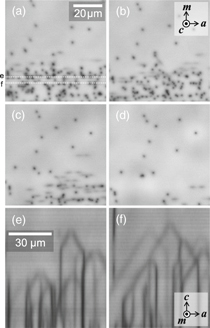
Fig. 4. 70 μm square MPPL images at the shallower level of Fig. 3(d) at (a) 108 μm depth, (b) 72 μm depth, (c) 36 μm depth from the surface, and (d) near the surface. Panels (e) and (f) show the cross-sectional MPPL images extracted from the 3D MPPL image from the white dotted lines "e" and "f" shown in Fig. 4(a), respectively, which indicate that two individual TDs over 50 μm apart moved towards each other as the growth proceeded, and finally disappeared.
Download figure:
Standard image High-resolution imageSubsequently, the Burgers vectors of these TDs were determined by bright field X-ray topography. Topographic images were taken directly by the forward transmitted X-ray beam passing through the cross-section of GaN crystals at the area illustrated as "Fig. 5" in Fig. 3(a) after thinning to less than 100 μm. In this paper, Burgers vectors of characteristic dislocations were investigated from topographic images of the dislocations on the basis of invisibility criterion of  where g is a diffraction vector and b is a Burgers vector of the dislocation. A series of the topographic images was captured in Figs. 5(a)–5(c) with (a)
  (b)
(b)  and (c)
  showing various dislocation images taken at the same area. Here, it can be seen that almost all dislocations are invisible in Fig. 5(a), but quite visible in Figs. 5(b) and 5(c). Previous studies have reported that dislocations of the (a + c)-type and those of the c-type were present in the GaN substrate in addition to those of the a-type,27,28) so the Burgers vectors of most dislocations were considered to be parallel to the a-axis. TD segments coming across each other, as in Fig. 4(e), were observed in Figs. 5(b) and 5(c). We describe three types: A-type, B-type, and C-type. It can be seen that two A-type TDs are visible in both Figs. 5(b) and 5(c), meaning that the Burgers vector of those TDs was parallel to the [
 ] direction. It can be estimated that those TDs having opposite Burgers vectors ([
 ] and [
 ]) propagated towards each other in the same (
 ) plane as the slip plane, and were annihilated after the reaction, as illustrated in Fig. 6(a). On the other hand, TDs described as B-type are visible in Fig. 5(b) and invisible in Fig. 5(c); meanwhile, those described as C-type were invisible in Fig. 5(b) and visible in Fig. 5(c), meaning that the Burgers vectors of the B- and C-types were parallel to the [
 ] direction and the [
 ] direction, respectively. At first glance, the topographic image appears to suggest that the B-type TDs exist on the (
 ) plane. However, given that the thickness of the specimen was about 100 μm, it is appropriate to assume that the B-type TDs actually exist in the (
 ) plane as shown in Fig. 6(b) and have opposite Burgers vectors ([
 ] and [
 ]), indicating the same annihilation phenomenon as A-type TDs. The TDs of C-type were also estimated to exist in the (
 ) plane. In summary, it was revealed that the TDD increased just after the coalescence of crystals, but was reduced by annihilation as growth proceeded.

Fig. 5. (Color online) A series of the topographic images with (a)  (b)
(b)  and (c)
  showing various dislocation images taken from cross-section of the sample at the same area.
Download figure:
Standard image High-resolution image
Fig. 6. (Color online) Schematic drawings of: (a) A-type TDs with opposite Burgers vectors ([1 10] and [
 ]) that were propagated towards each other in the same (
 0) plane as a slip plane and then annihilated after the reaction; (b) B-type TDs with the other opposite Burgers vectors ([2
 ] and [
 ]) also propagated towards each other in the same (
 0) plane as a slip plane; (c) a model of the generation of the TDs that were annihilated in a later growth stage, showing that two TDs of edge character propagating along the c-axis with opposite Burgers vectors along the ±a-axis were generated at both edges of a BPD with a screw character.
Download figure:
Standard image High-resolution image
Finally, we discuss the mechanism of dislocation annihilation. Generally, annihilation occurs in a crystal with high TDD on the order of 1010 cm−2,29,30) in which the distance of neighboring TDs is about 100 nm. Therefore, the annihilation of TDs over 50 μm away from each other observed in this study is considered a unique phenomenon in the Na-flux method. However, for the annihilation to occur, two TDs must have opposite Burgers vectors and exist on the same slip plane, as mentioned above. We therefore doubted that completely separate TDs over 50 μm away could have those exact characteristics by chance. Here, we estimated that those TDs were generated at the same place and annihilated in a later growth stage, and we proposed a model for their generation as illustrated in Fig. 6(c). Many BPDs were generated around the coalescence boundary, as seen in Figs. 3(e) and 3(f). They had the Burgers vector parallel to the a-axis, as seen from the topographic images in Figs. 5(a)–5(c), and were estimated to have a screw component. If a part of a BPD moved to the c-direction in an m-plane, two TDs of edge character propagating along the c-axis with opposite Burgers vectors along the ±a-axis could be formed at both edges of the BPD. Once the BPD reached the surface of the crystal after additional movement, the residual strain between the two TDs was relieved, and a pair of two separate TDs with an edge character was generated. These TDs propagated in the same m-plane as the slip plane, so they could react again and annihilate each other. However, this is only a simple model. Actually, given that the movement of a part of a BPD occurs at several time points, many more kinks could be formed during the growth, resulting in the generation of many more than one pair of TDs. The reasons for the BPD movement and annihilation at the later growth stage remain to be clarified. We will continue to investigate the triggers of those phenomena.
In this study, we fabricated a GaN wafer with the point-seed technique, and carefully investigated the behavior of TDs in the wafer. It was discovered for the first time that a large number of dislocations were generated at some coalescence boundaries of the crystals, but that a portion of them disappeared by annihilation as growth proceeded, which is one of the mechanisms for reduction of the TDD. The separation of dislocations by lateral propagation as BPDs is also considered to be a mechanism for the reduction of density. Dislocations were considered to diverge as a pair of TDs from a BPD generated from a coalescence boundary. Thus, we estimated that the large number of dislocations increasing at the coalescence boundary also included pairs of TDs generated in excess, which reacted with and annihilated each other in a later growth stage. As a result, TDD of more than 106 cm−2 did not exist on the surface.
Acknowledgments
We gratefully acknowledge funding from the Japan Science and Technology Agency (Grant No.: JPMJAL1201) and from the Ministry of the Environment. Topographic images were taken at the BL24XU of SPring-8 with approval from the Japan Radiation Research Institute (Proposal No. 2019A3202).