

Abstract
For developing high performance thermoelectric materials based on anomalous Nernst effect (ANE), we propose a ferromagnetic metal/semiconductor multilayer, where ferromagnetic metal/semiconductor interfaces prevent heat carrier transport (thermal conductivity reduction), and are expected to enhance the ANE coefficient additionally. The amorphous Co/Si multilayer displays an extremely-low thermal conductivity of ∼1.5 Wm−1 K−1 due to the interface phonon scattering and undoped Si amorphous layers with low thermal conductivity. Concurrently, the multilayers exhibit 2.4 times larger anomalous term of transverse Seebeck coefficient than Co films. This demonstrates that the nanostructure with the ferromagnetic metal/semiconductor interfaces is beneficial for developing thermoelectric generation based on ANE.
Export citation and abstract BibTeX RIS
Thermoelectric (TE) conversion, which generates electricity from wasted heat, has drawn considerable attention as one of the energy harvesting technologies. In addition to a representative Seebeck effect-based TE conversion, the conversion based on anomalous Nernst effect (ANE) has recently drawn much attention. 1–7) According to the recent report, 1) TE conversion efficiency based on ANE can be higher than that based on Seebeck effect in the case of the same dimensionless figure-of-merit. However, the dimensionless figure-of-merit for ANE (ZTANE) is quite small (∼0.001) 1,8–10) compared with that for Seebeck effect in general.
For increasing ZTANE, described as QANE 2(μ0 M)2 σ yy T/κ, most of the research groups have enthusiastically worked on increasing anomalous term of transverse Seebeck coefficient (SANE = QANE μ0 M), where QANE is anomalous Nernst coefficient, μ0 is vacuum permeability, M is magnetization, κ is thermal conductivity, σyy is electrical conductivity and T is absolute temperature. Nakatsuji et al. experimentally found that the increase of the SANE is likely attributed to Berry curvature near Fermi level. 6,8,11) Other groups have observed that SANE was increased by the ferromagnetic metal/paramagnetic metal interface effect such as magnetic proximity effect and spin–orbit interaction or by nano-sized granular structures, etc., 12–17) the detail of which mechanism remains unclear. Although various methodologies for high SANE have been suggested, nobody has paid attention to κ reduction for increasing ZTANE because it is difficult to reduce κ in metal with inherently-high κ.
We have developed the TE semiconductor materials based on Seebeck effect, which have low κ by nanostructuring approach: 18–28) ∼0.78 Wm−1 K−1 for connected Si nanodots, ∼3 Wm−1 K−1 for Si/Si1−x Gex superlattice, etc. This κ reduction is yielded by the introduction of nanostructured interfaces working as phonon scattering centers into the semiconductor where the main heat carrier is phonon. If the aforementioned κ reduction, caused by the semiconductor nanostructured interfaces, could also be applicable to metal with ANE, and there could be the interface effect for SANE enhancement in metal/semiconductor system, ZTANE value would be greatly increased.
In this study, we propose a ferromagnetic metal/semiconductor multilayer, where a ferromagnetic metal/semiconductor multilayer interface prevents heat carrier transport (κ reduction), and is expected to increase SANE additionally (Fig. 1). For this demonstration of the nanostructure design, we focus on Co with relatively-high Curie temperature as a ferromagnetic metal and Si as a representative ubiquitous semiconductor. The amorphous Co/Si multilayer films (MLF) exhibit an extremely-low κ of ∼1.5 Wm−1 K−1 thanks to both the interface phonon scattering and the contribution of amorphous Si with inherently-low κ. A remarkable fact is that the κ is reduced even in ferromagnetic metal/semiconductor multilayer, which is beneficial for developing ANE-based TE materials with high ZTANE. Furthermore, we also observe the 2.4 times SANE enhancement by the introduction of metal/semiconductor interface. This study opens a renewed avenue for the development of TE generation based on ANE.
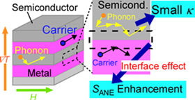
Fig. 1. (Color online) Schematic of ferromagnetic metal/semiconductor multilayer. Therein, κ reduction is brought by both the interface phonon scattering and the contribution of semiconductor with inherently-low κ. The enhancement of SANE is also expected by the interface effect.
Download figure:
Standard image High-resolution imageThe samples were fabricated by electron beam deposition using high purity Si (99.999%) and Co (99.9%) sources as follows. Undoped Si(001) substrates were cleaned by a standard wet chemical process and hydrogen-terminated Si surfaces were prepared by HF solution. The cleaned Si substrates with a size of 6 × 7 × 0.3 mm3 were introduced into vacuum chamber at a base pressure of ∼1 × 10⁻⁴ Pa. The amorphous Co/Si MLFs were grown on the Si substrates at room temperature (RT) by alternately depositing Co and Si, where each layer thickness was 20 nm; namely periodicity was 40 nm and MLF thickness (L) was 40 nm × (periodic number). For reference, we also formed amorphous Co films with a thickness of 20 nm on the Si substrates (CF) at RT.
The cross-sectional sample structures were observed using scanning electron microscopy (SEM) with a 10 keV electron beam. The amorphous phase was confirmed by X-ray diffraction (XRD) with Cu Kα line (wavelength: 0.15418 nm). The out-of-plane κ values of the MLF (κMLF) were measured by 2ω method 18–20,23,25) (TCN-2ω, Advance Riko Inc.) which is a κ measurement technique based on the thermoreflectance method with periodic heating. The 2ω method was performed at RT under vacuum (∼1 Pa) using a laser with a wavelength of 635 nm and the heating electric current with the frequency from 1 to 5 kHz, where Mo films (100 nm) as transducer and SiO2 films (18 nm) for insulating were deposited on the sample surfaces by RF sputtering. The in-plane σ yy and Seebeck coefficient (SSE) values were measured at RT using van der Pauw method and ZEM-3 (ADVANCE-RIKO Inc.), respectively. The transverse Seebeck coefficient (S yx ) was obtained from the VNE/d∇T in perpendicular magnetized (PM) configuration, where VNE is transverse TE voltage and d is measurement distance. 2) The VNE was measured at RT using physical property measurement system (PPMS). The VNE is usually measured using PM or in-plane magnetized (IM) configurations [Fig. 2(a)], where the directions of T gradient, magnetic field (H), and the VNE are perpendicular to each other. In IM configuration of multilayers, it is well-known that spin Seebeck effect appears in addition to ANE, making it difficult to understand the physics of SANE enhancement. On the other hand, in PM configuration, we can measure the VNE coming from only ANE because spin Seebeck effect does not appear. 29) In this study, to discuss SANE enhancement easily, we used PM configuration shown in Fig. 2(a), where the VNE along the y direction was measured when applying T gradient along the x direction and H along the z direction. The Hall resistivity (ρ yx ) in the in-plane direction was measured by Hall effect measurement. We also measured M curves of samples with magnetic property measurement system (MPMS3).
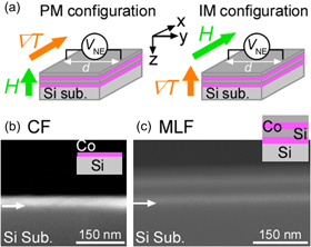
Fig. 2. (Color online) (a) Schematics of PM and IM configurations. In PM configuration, when applying T gradient along the x direction and H along the z direction, the VNE along the y direction was measured. In IM configuration, when applying T gradient along the z direction and H along the x direction, the VNE along the y direction was measured. d is measurement distance. (b), (c) SEM images of the CF (b) and the MLF (c) with their schematics. The arrows in (b) and (c) indicate the interfaces between film and substrate.
Download figure:
Standard image High-resolution imageFigures 2(b) and 2(c) show cross-sectional SEM images of CF and MLF with periodic number of 2, respectively. It was confirmed that the total thicknesses of MLF and CF samples were ∼80 and ∼20 nm, respectively, and each layer thickness of MLF was ∼20 nm. In addition, as denoted by the arrows in Figs. 2(b) and 2(c), the interfaces between film and substrate were sharply formed. The XRD proved that these samples were amorphous (not shown). Thus, it was found that samples were formed as amorphous films.
Mo films for transducer and SiO2 layers for insulating were deposited on the MLFs for 2ω method. Total thermal resistance (Rtotal) of SiO2/MLF was acquired as shown in Fig. 3(a). In thermal circuit model, Rtotal is described as L/κMLF + RSiO2 + ITRMo/SiO2 + ITRSiO2/MLF + ITRMLF/sub, where RSiO2, ITRMo/SiO2, ITRSiO2/MLF, and ITRMLF/sub, are thermal resistance of SiO2 layer and interfacial thermal resistances at the Mo/SiO2, SiO2/MLF, and MLF/substrate interfaces. The linear dependence in Fig. 3(a) validated thermal circuit model in the present MLFs with 40 nm periodicity. Using the slope of L dependence of Rtotal in Fig. 3(a), κMLF was acquired to be ∼1.5 Wm−1 K−1. Figure 3(b) summarizes the experimental κMLF (MLF exp.), the reported κ value of bulk Co 30) (BC), the calculated κ value of CF (κCo) and the calculated κMLF (MLF cal.) at RT. Therein, the out-of-plane κCo was calculated to be 47 Wm−1 K−1 from Wiedemann–Franz law (L0 Tσ yy ), where in-plane σ yy of CF was measured to be 6.4 × 10⁻⁴ Ω−1 cm−1 and L0 is Lorenz number, by assuming that there is no anisotropic electrical conductivity in the amorphous CF. The calculated κMLF was estimated (2.9–4.9 Wm−1 K−1) using a series thermal resistance model described as L/κMLF = L/2κCo + L/2κSi, where κSi is the κ value of Si film (1.5–2.6 Wm−1 K−1). 31–34) In the calculated κMLF, the interfacial thermal resistance at the Co/Si interface (ITRCo/Si) is not included. The experimental κMLF was ∼31 times smaller than that of κCo, which is mainly attributed to the contribution of amorphous Si layer with smaller κ. Note that the experimental κMLF was smaller than the calculated one without ITRCo/Si. This experimental fact indicates that Co/Si interface plays some role for κ reduction.

Fig. 3. (Color online) (a) Rtotal of the MLFs as a function of MLF thickness L (=40 nm × periodic number). (b) Thermal conductivities of the MLF, the CF, and bulk Co: experimental κMLF (MLF exp.), the reported κ value of bulk Co 30) (BC), the calculated κCo (CF), and the calculated κMLF (MLF cal.). The calculated κMLF was estimated based on a series thermal resistance model without ITRCo/Si.
Download figure:
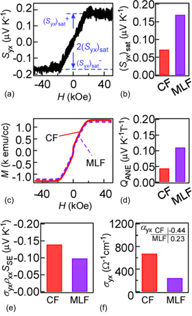
Standard image High-resolution imageFigure 4(a) shows S yx –H curve in PM configuration. S yx value includes normal and anomalous terms of transverse Seebeck coefficient. To remove the normal term of S yx , here, the anomalous term of S yx is experimentally obtained as (S yx )sat = (∣(S yx )sat + − (S yx )sat −∣)/2, where (S yx )sat + and (S yx )sat − are the intercepts determined by extrapolating fitted line functions in positive and negative high H ranges (M saturation region) to zero field in S yx –H graph, respectively. Figure 4(b) summarizes (S yx )sat values of the MLF with periodic number of 2 and the CF. Intriguingly, the MLF exhibited 2.4 times larger (S yx )sat than the CF. So far, the enhancement of (S yx )sat had been reported only in ferromagnetic metal/paramagnetic metal multilayers. 12–14) This result demonstrated that (S yx )sat was enhanced even in ferromagnetic metal/semiconductor multilayer. It is considered that electrical current flows almost only in Co layers in MLF because of undoped Si layers with high resistivity. The σ yy in CF (6.4 × 10⁴ Ω−1 cm−1) was twice larger than that (3.2 × 10⁴ Ω−1 cm−1) in MLF with the layer thickness ratio of Co (20 nm)/Si (20 nm) of ∼1, revealing that Co layers in MLF have almost the same σ yy as the CF.
Fig. 4. (Color online) (a) S yx –H curve in the MLF. (b) (S yx )sat of the CF and the MLF. (c)–(f) Properties of the CF and the MLF measured in PM configuration: (c) M–H curves, where M is obtained using total thickness of Co layers in samples, (d) QANE values, (e) σ yx ρ xx SSE values, and (f) σ yx values where σ yx is obtained using total thickness of samples and estimated α yx values in inset.
Download figure:
Standard image High-resolution image
Now, we consider the origin of (S yx )sat enhancement. First, we checked saturation magnetization (MS) because (S yx )sat is basically proportional to the μ0 MS. The M–H curves of the MLF and the CF in PM configuration in Fig. 4(c) revealed that the both samples have almost the same MS values, indicating that (S yx )sat enhancement does not come from MS increase. Actually, QANE, which is obtained as (S yx )sat divided by μ0 MS, exhibits the 2.6 times larger value in the MLF than that of the CF as shown in Fig. 4(d). Next, we consider the Hall effect contribution. The (S yx )sat is described as (S yx )sat = ρ xx α yx + ρ yx α xx , where α xx and α yx are longitudinal and transverse TE conductivities, respectively, 35) and ρ xx is longitudinal electrical resistivity. When the approximation that ρ xx ≫ ρ yx and α xx = SSE /ρ xx works out, (S yx )sat is written as follows:

where the σ yx is the anomalous Hall conductivity. It is known that the second term of Eq. (1) comes from Hall effect of Seebeck effect-induced charge current. On the other hand, the first term of Eq. (1) is a direct generation of transverse charge current originating from α yx . Therefore, there is a possible mechanism that the (S yx )sat enhancement comes from σ yx ρ xx SSE increase owing to contribution of high SSE of Si. However, as shown in Fig. 4(e), the enhancement of σ yx ρxx SSE value in the MLF was not observed, indicating that the (S yx )sat enhancement does not come from enhancement of the Hall effect due to high SSE of Si. Furthermore, it is also difficult to explain the present enhancement effect by the effect of the spin–orbit interaction at the interface 16) because of the light element Si. Next, as a mechanism for (S yx )sat enhancement, we consider the increase of Berry curvature at the metal/semiconductor interfaces. The increment of Berry curvature function [Ω(E)] with a variable of electron energy (E) increases the second term of Eq. (1) (SSE < 0) because σ yx is proportion to integrated Ω(E) in the range of E less than Fermi energy. 36–39) However, as shown in Fig. 4(f), it was not confirmed that the σ yx value [=−ρ yx /(ρ yx 2 + ρ xx 2)], which were obtained from measurement values (ρ yx and ρ xx ), increases in the MLF. However, there is still a possibility that increment of Berry curvature Ω(EF) at Fermi energy (EF) increases αyx because α yx is proportional to Ω(EF). The inset in Fig. 4(f) shows larger estimated α yx in MLF, indicating that the increment mechanism of Ω(EF) cannot be excluded. Although the increment of Ω(EF) can explain (S yx )sat enhancement, there can also be other mechanisms: magnetic proximity effect mechanism at the ferromagnetic metal/semiconductor interface or other mechanisms. The similar magnetic proximity effect was observed in conformable multilayer systems with the ferromagnetic metal/paramagnetic metal interfaces. 12–14) The study about the mechanism will be done in the future.
In summary, we demonstrated that κ was reduced even in amorphous ferromagnetic metal (Co)/semiconductor (Si) multilayer. Therein, the extremely-low κMLF of ∼1.5 Wm−1 K−1 was brought by both the interface phonon scattering and the contribution of amorphous Si with inherently-low κ. Furthermore, we also observed the (S yx )sat enhancement. These results give us a beneficial knowledge for developing ANE-based TE material with high ZTANE using metal/semiconductor interfaces.
Acknowledgments
This work was partially supported by JST-CREST (Grant No. JPMJCR1524). This work was also partially supported by a Grant-in-Aid for Science Research A (Grant No. 17H01052, 18KK0377, 19H00853) and for Exploratory Research (19K22110), the Murata Science Foundation, CASIO Science Promotion Foundation (37-01), the Center for Spintronics Research Network (CSRN), and Collaborative Research Center on Energy Materials (E-IMR). A part of electron beam deposition and RF sputtering in this work was supported by "Nanotechnology Platform Project (Nanotechnology Open Facilities in Osaka University)" of Ministry of Education, Culture, Sports, Science and Technology, Japan (No. F-20-OS-0030 and No. S-20-OS-0024).