
Abstract
This review introduces the latest progress on gallium nitride (GaN)-based visible vertical-cavity surface-emitting lasers (VCSELs) with features such as plane and curved distributed Bragg reflectors (DBRs) made of dielectric materials and boron ion implantation to form current apertures. This novel class of GaN-based VCSELs allow small apertures down to 3 μm and long cavities of more than 20 μm without the occurrence of diffraction loss. These structures have enabled low threshold currents (e.g., Ith = 0.25 mA), high efficiency operation (e.g., WPE = 9.5%), and robust fabrication processes with high lasing yield. All those characteristics are the best among those previously reported GaN-based VCSELs. The proposed structure should facilitate the production of VCSELs formed on semi-polar plane GaN substrates and arrayed VCSELs, which are expected to realize novel light emitters that have been previously difficult to fabricate, such as green VCSELs and watt-class blue VCSEL arrays.
Export citation and abstract BibTeX RIS

Content from this work may be used under the terms of the Creative Commons Attribution 4.0 license. Any further distribution of this work must maintain attribution to the author(s) and the title of the work, journal citation and DOI.
1. Introduction
Gallium nitride (GaN)-based light emitting devices, LEDs and edge-emitting lasers (EELs),1,2) have attracted significant interest from researchers. The wide bandgap of GaN-based materials allows emission covering a wide range of wavelength from UV to green, which was not capable with classically available direct band-gap materials such as arsenides and phosphides. Recently, GaN-based vertical-cavity surface-emitting lasers (VCSELs)3) are receiving much attention. The advantages of VCSELs, such as a low threshold current, arraying capability, and applicability to high-frequency operation, provide the possibility of GaN-VCSEL application as light sources for optical storage, laser printers, projectors, displays, solid-state lighting, optical communications, and biosensors, among many others.
This is a Progress Review focusing on the latest results of the authors' research on the development of GaN-based VCSELs.4–10) A low threshold current is the most prominent and representative feature of these VCSELs, so that the approach of this research is to further enable such capability. The proposed structure has features of an extremely long cavity of 20 μm or more, plane and curved distributed Bragg reflectors (DBRs) made of dielectric materials, and boron ion implantation (BII) to form current apertures [see Fig. 1(a)]. Such an approach is completely different from that conventionally taken in GaAs-based VCSELs,11) where two flat and conductive semiconductor DBRs form a short cavity and current paths, and the lateral oxidation of the AlAs layer is used for aperture formation [see Fig. 1(b)]. At the International Workshop on Nitride Semiconductors held in Kanazawa, Japan, 2018 (IWN2018), we reported a low threshold current much less than 1 mA with the proposed structures.9,10) The main purpose of this review is to introduce those results.
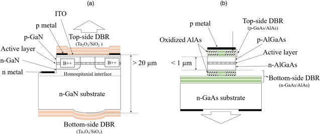
Fig. 1. (Color online) Schematic diagrams of a (a) GaN-based VCSEL, the focus of this review, and (b) a typical GaAs-based VCSEL.11)
Download figure:
Standard image High-resolution imageThe contents of this review are as follows. Section 2 introduces the brief history of VCSELs. Section 3 reviews previous literature on GaN-based VCSELs and provides a detailed background to this study. In Sects. 4 through 6, the latest progress of the authors' research is given. These sections introduce how successfully BII and a long cavity with plane and curved mirrors confine carriers and photons, both in the vertical and lateral directions. Section 7 discusses contemporary and future work, and the last section gives conclusions.
2. Background
Laser action is based on stimulated emission, proposed by Einstein one hundred years ago,12) where the density of photons and excited states enhances the formation of new photons. Thus, confinement of all those in the same space is the essence of lasers. In VCSELs, firstly proposed by Iga in 1977,3) a photon is vertically confined within a cavity by mirrors placed on both sides of it. The cavity of a VCSEL holds quantum wells (QWs) to provide vertical confinement of the carriers within themselves. The precursory work of Iga and colleagues triggered intensive research on VCSELs in the 1980 s and '90 s. Among VCSELs based on a variety of materials, GaAs-based VCSELs have had the greatest success. AlGaAs-based DBRs, where layers of AlGaAs with two different compositions are periodically laminated,13) offer reflectivity close to 100%, which allows efficient confinement of photons in the vertical direction. It is convenient that such AlGaAs-based DBRs can serve as current paths under doping with p- or n-type impurities. The selective oxidation of the AlAs layer placed adjacent to the QWs has also provided progress of VCSELs by the implementation of lateral confinement, both of light and carriers.14) In all of these works given here, metalorganic chemical vapor deposition (MOCVD) and molecular beam epitaxy have enabled precise control of the vertical structure of the cavity, such as the length and position of the QWs. Thereby, the antinode of the cavity mode can easily overlap the QWs. With all these approaches, GaAs-based VCSELs possess a perfect set of confinements in both the vertical and lateral directions to bound photons and carriers into the limited space of the QWs as the active region of the device. The realization of these conditions has enabled highly effective15) and stable fabrication of VCSELs over GaAs wafers. Nowadays, GaAs-based VCSELs form a very large market, which is predicted to reach 3.5 billion US dollars by 2023.16)
3. Previously reported GaN-based VCSELs
GaN-based VCSELs have still remained in a research phase. This is mainly due to difficulty in the fabrication of GaN-based vertical cavities. This section reviews previous studies on GaN-based VCSELs with respect to the following key factors:
- DBR mirrors,
- control of vertical structures in cavities,
- structures that enable lateral carrier and optical confinements.
All of these factors are required to provide photon and carrier confinements in the active region. In the following sections, reasons why these structures are proposed are given, where dielectric DBRs, long cavities, curved mirrors, and apertures with BII are incorporated.
3.1. DBR mirrors
Mirrors are important components for VCSELs to provide vertical confinement of photons. In VCSELs, the mirror reflectivity must be comparable to or greater than 99% to allow laser operation. This is due to the limited amount of gain. Figure 2 shows calculated curves that explain how the VCSEL amplification rate is dependent on the total thickness and material gain of the QWs, which commonly serve as an active region. Assuming the typical thickness and gain of QWs are, for example, 12 nm and 2000 cm−1,17) respectively, amplification would be approximately 1%. This demands high reflectivity of mirrors in VCSELs. In particular, reflectivity close to 100% is favorable to achieve a low threshold current.

Fig. 2. Estimated amplification rate per round trip calculated for material gain and total effective thickness of active region. In this review, QWs are supposed to provide an active region and the enhancement factors are to be two. Please see appendix A for details of the calculation.
Download figure:
Standard image High-resolution imageThus, DBRs, where numbers of periodically laminated layers offer reflectivity close to 100%, are often used with VCSELs. Previous reports on GaN-based VCSELs introduce a few categories of DBRs, of which nitride semiconductor DBRs18–22) have been of the greatest interest. In 2008, Ref. 23 reported the first example of continuous wave (CW) lasing from a GaN-VCSEL, in which the bottom-side DBR comprised 29 AlN/GaN bilayers grown directly on a c-orientated GaN substrate by MOCVD. In this device, a half-wavelength AlN/GaN super lattice stack was inserted between every four pairs of AlN/GaN quarter-wavelength stacks to produce the DBR and avoid cracks caused by the lattice mismatch between AlN and GaN. Researchers at École polytechnique fédérale de Lausanne (EPFL) make use of Al0.82In0.18N layers lattice-matched to GaN instead of AlN to enable a crack-free bottom DBR and have reported pulsed operation.24) Researchers at Meijo University have reported CW operation on the device with the similar structures.25–27) Semiconductor DBRs are widely used for commercially available GaAs-based VCSELs. These structures enable consecutive growth of all structures inside a cavity, including top-side DBRs.
However, all these examples.23–27) introduce dielectric materials formed by vacuum deposition for the top-side DBRs, thereby avoiding epitaxially grown nitride-based DBRs. The reason for this is the high activation energy of p-type dopants in high Al-content nitride semiconductors (e.g., 510 meV).28,29) Instead, intracavity contact made of a thin (20–30 nm) indium tin oxide (ITO) layer placed between the p-GaN spacer layer and the top-side dielectric DBRs is used to establish a current path from the top side of the device.23–27,30–37)
There are many reports where both-side DBRs are composed of dielectric materials, which are referred to as all-dielectric DBR VCSELs. As early as 2008, researchers at Nichia Corporation achieved CW operation of blue-violet all-dielectric DBR GaN-based VCSELs.30) In this approach, they prepared a c-orientated sapphire wafer covered with a MOCVD-grown n-type layer, QWs, a p-type layer, vacuum deposited thin ITO and dielectric DBRs. They bonded the top side of the wafer to a supporting wafer and removed the sapphire using laser lift-off (LLO). After polishing the bottom-side of the wafer, a dielectric DBR for an n-side mirror was subsequently deposited there. In their following studies using GaN substrates,31) CW and pulsed operation were achieved for 510 and 529 nm, respectively.32) This approach has been associated with similar studies from multiple organizations, such as Panasonic,33) Xiamen University,34) and University of California Santa Barbara (UCSB).35,36)
Dielectric DBRs have high quality as reflectors. Figures 3 and 4 show the calculation results for DBR reflectivity and stopband width (see appendix B for the calculation details). In Fig. 4, the stopband width is normalized by λ0, the wavelength gives the peak reflectivity of DBRs, which equals to quadruple of the light path of each layer of the DBRs. The DBR reflectivity and stopband width have positive correlation to the refractive index difference of the materials that constitute the DBR. Dielectric DBRs made by combining, for example, Ta2O5 (or SiN) and SiO2 that have a large difference in refractive index allows them to be efficient as reflectors. On the other hand, the small difference in the refractive indices between nitride semiconductors means that DBRs made of those materials must lead to a narrow stopband less than 10% of λ0, and thus require a large number of pairs (more than 20 at least) to attain higher reflectivity than 99%.
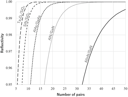
Fig. 3. Calculated reflectivity for numbers of pairs that comprise the DBR, where a variety of materials used. See appendix B for the calculation details.
Download figure:
Standard image High-resolution image
Fig. 4. Calculated relation between refractive index difference and width of stopband normalized by λ0 (quadruple of the light path equivalent to the thickness of each layer of the DBRs). See appendix B for the calculation details.
Download figure:
Standard image High-resolution imageThis narrow stopband is a remarkable issue. Nitride semiconductor DBRs tend to have stopbands even narrower than arsenide. This narrow stopband requires strict control of the thickness of each layer of nitride DBRs within a few percent37) to keep the stopbands within the lasing wavelength. In addition, it was reported that the growth rate for AlInN is so low that it takes 12 h to grow DBRs with 40 AlInN/GaN DBRs bilayers.25) These have been barriers to prevent GaN-based VCSELs from mass production. Thus, the present authors determined to use dielectric DBR to form both sides of the cavity.
3.2. Control of vertical structures in the cavity
In VCSELs, appropriate formation of the vertical structures of the cavity, including p- and n-type spacer layers, QWs and other intracavity layers, is of significant importance to determine the cavity length, cavity mode wavelength, and vertical positions of antinodes and QWs. However, precise control of these is not easily achieved in the fabrication processes of all-dielectric DBR VCSELs.
In previous reports on GaN-based VCSELs,23–36) the light path between QWs and the reflecting surface of the top-side DBR is designed to be close to the lasing wavelength so that the antinodes overlap the QWs in the vertical direction. The thickness of these layers is finely controlled by MOCVD and vacuum deposition at a nanometer level. Thus, the remaining concern is controllability of the cavity length that defines the wavelength of the cavity mode. Previous all-dielectric DBRs GaN-based VCSELs30–36) have adopted a variety of processes to remove the substrate, such as LLO,30,31) chemical mechanical polishing,31–34) and photoenhanced chemical etching.35,36) However, many studies with relatively low threshold current adopt polishing processes to flatten the back surface of the wafer before fabrication of the bottom-side DBR.30–34) Otherwise, the operation of the device resulted in high threshold current under pulsed injection.35,36) Reference 38 reported that sub-nanometer smoothness is required to suppress roughness-derived scattering. Thus, the polishing processes are essential. However, Ref. 31 reported a considerable shift between the experimental target cavity length (ca. 1 μm) and the results (ca. 4 μm) due to instability of the polishing rate. This often causes displacement between the wavelength of the cavity mode and the desired wavelength, which is related to the distance between the QWs and reflecting surface of the top-side DBR. Difficulty in controlling the cavity length has thus been a severe barrier to the mass production of this type of device.
Adopting a longer cavity could solve this problem. As shown in Fig. 5, the longitudinal mode spacing is the reciprocal of the cavity length. Thus, a long cavity allows for the device to select a longitudinal mode that favorably overlaps with the QWs, even though the cavity length is not controlled. For example, a 20 μm long cavity has longitudinal modes with 2 nm separation, which gives negligible displacement from the optical distance between the reflecting surface of the top DBR and QWs, thought to be 400–450 nm in blue or violet VCSELs.
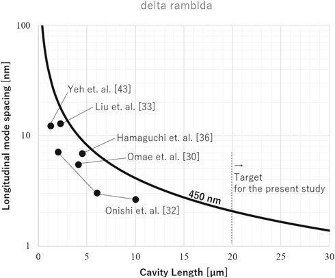
Fig. 5. Experimental and theoretical plots for cavity length and longitudinal mode spacing. Theoretical data were calculated by assuming λ (wavelength) at approximately 450 nm, n (refractive index) at 2.45, and dn/dλ at 0.001.6) Almost all experimental data are plotted below the calculated line. This is considered to be because the cavity length shown in each literature-reported value omitted the penetration depth to the DBRs. The lasing wavelength shorter than 450 nm used for calculation should be another factor that shifts these data points to a lower position on this graph.
Download figure:
Standard image High-resolution imageBased on this discussion, the authors compromised with instability in control of the cavity lengths and decided to adopt cavities longer than 20 μm for devices, which is considerably longer than previously reported values (data shown in Fig. 5).
3.3. Lateral carrier and optical confinements
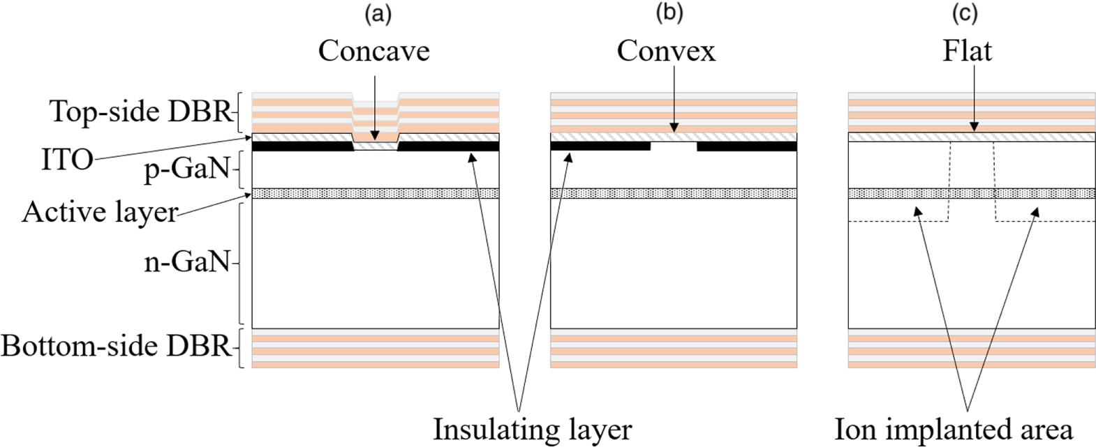
This section argues the lateral confinements of carrier and cavity modes. Almost all the previously reported structures of GaN-based VCSELs have flat bottom mirrors and no lateral variation of refractive indices, except for around the top-side DBRs. Thus, the configuration around the top-side DBR is the key to categorize the propagation behavior. There are three types that have been reported: concave, convex and flat [see Figs. 6(a)–6(c), respectively].
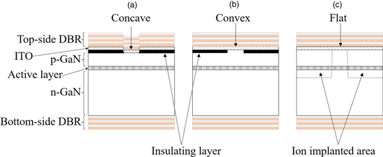
Fig. 6. (Color online) Schematic diagram for typical cavity structures of previous GaN-based VCSELs; (a) concave, (b) convex, and (c) flat configurations in the top-side DBR dimension.
Download figure:
Standard image High-resolution imageEarly, concave top-side DBRs have been major structures for lateral current confinement, where an insulating layer such as SiO230–33) or SiN25,35) is partially inserted between the p-GaN and ITO layers. Such insulators are patterned to leave a circular aperture with a diameter from 7 to 20 μm for laterally confined current injection. References 39, 40 studied the effect of those structures on the lateral optical loss using numerical simulations. They concluded that a concave structure forms an anti-guiding cavity with a larger diffraction loss than other types, flat and convex structures.
Reference 41 reported GaN-based VCSELs with aluminum-ion implanted apertures to achieve a flat configuration of the top-side DBR [see Fig. 6(c)] and reported a five-fold reduction in threshold current of the device under pulsed injection when compared with a concave structure. This result experimentally endorsed the simulated results predicted by Refs. 39,40. Reference 37 reported CW operation of GaN-based VCSELs with a flat structure aperture by BII, for a unique cavity structure where the bottom-side mirrors are engulfed inside n-type GaN grown by epitaxial lateral overgrowth.42) However, no discussion on the contribution of BII to the device characteristics was given there.
Recently, experimental studies are revealing that convex structures, as well as flat structures, are effective to improve the cavity quality of GaN-based VCSELs. Researchers at National Chiao Tung University (NCTU) confirmed that an etched mesa structure [see Fig. 6(b)] has an effect of lateral optical guiding.43) Members of the National Taiwan University of Science and Technology (NTUST) in collaboration with NCTU later reported CW operation with a convex structure where the p-GaN layer was etched to a depth of 15 nm by reactive ion etching (RIE).44) The latter research achieved a threshold current of approximately 0.5–0.6 mA, which was the lowest record for a GaN-based VCSEL. Reference 27 confirmed the effect of lateral optical guiding for a convex structure obtained by inserting a 30 nm thick Nb2O5 disk between the ITO and top-side DBR, just above the current aperture. In 2018, researchers at Stanley Electronics collaborated with Meijo University achieved a 4.7-fold improvement of the slope efficiency (SE),45) based on an approach similar to that of NTUST and NCTU. Reference 46 from that team have reported a blue VCSEL with a similar structure that provides a peak output power of 15.8 mW and a wall plug efficiency (WPE) of 8.9%, which is the records for the highest output and efficiency. It is notable that all the GaN-based VCSELs enabled records for the lowest threshold current and the highest output and efficiency with an adopted convex structure.
The results from NTUST and NCTU44) and Meijo University27) are significant as experimental efforts to miniaturize GaN-based VCSELs. These devices with convex structures have enabled CW operation of devices with small aperture diameters such as 3, 5,44) and 6 μm,27) which are the smallest among all the other reports. Although shrinkage of the aperture is effective to reduce the threshold current, theory predicts that diffraction becomes prominent for devices with smaller beam waists (see Fig. 7 and appendix C for details on the theoretical analysis of diffraction). Thus, researchers make use of convex structures with the expectation of optical guidance to reduce diffraction loss for devices with such small diameters as 3–6 μm.

Fig. 7. Calculated diffraction loss per round trip for a cavity with two plane mirrors. Here, the beam waist and cavity length are chosen as the parameters critical to diffraction. Please see appendix C for details of this calculation.
Download figure:
Standard image High-resolution imageHowever, there remains some problems regarding aperture shrinkage with these step-like convex structures. Figure 8 shows the threshold current density (Jth) as a function of the aperture diameter obtained from previous reports. This figure shows only selected data giving Jth less than 10 kA cm−2. A negative correlation between Jth and the aperture sizes of the devices is observed. The possible factors for this tendency are the induction of carrier loss or optical loss with aperture shrinkage. Focusing on the optical effect, these step-like structures may not have implemented ideal lateral optical confinement to perfectly nullify the diffraction of resonant modes. Another possible factor is scattering loss due to steps that should deteriorate the device characteristics with shrinkage in the aperture diameter. Moreover, longer cavities, e.g., 20 μm, which are proposed in the former section, cause diffraction losses to become even greater. This further emphasizes the importance of the convex structure to allow flawless waveguiding.
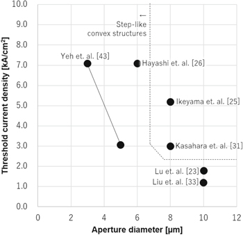
Fig. 8. Selected data of threshold current density (Jth) as a function of the designated current aperture diameter for CW-operated GaN-based VCSELs. Here, examples with Jth lower than 10 kA cm−2 are selected and plotted.
Download figure:
Standard image High-resolution imageBased on the discussion so far, the authors determined the approach to the lateral structures for the study as follows. First, a flat configuration for top-side DBRs is adopted with an aim to avoid concave and step-like convex structures that are associated with Jth deterioration upon shrinkage of the apertures. The authors decided to search for other convex structure with advantages as optical guides to enable low threshold operation with small apertures and long cavities.
3.4. Summary for previously reported GaN-based VCSELs
Based on the discussion of previous reports on GaN-based VCSELs, the present study adopted the following approaches: (i) dielectric materials are used to compose DBR mirrors on both sides of the device because of their high quality as reflectors. This choice enabled the fabrication process to avoid concern of severe layer thickness control, which is associated with the formation of nitride semiconductor DBRs. (ii) Cavities longer than 20 μm are used to obtain dense longitudinal mode spacing. This eliminates the requirement of precise cavity length control, which is associated with all-dielectric DBR VCSELs with cavities shorter than several micrometers. (iii) A flat configuration is adopted for the top side to avoid optical loss generated by convex and step-like concave structures. The authors decided to seek another convex structure to nullify diffraction loss that allows small apertures less than several micrometers.
All of these approaches were determined with the intention to obtain a structure that allows low threshold currents and stable fabrication processes for GaN-based VCSELs.
4. Lateral optical confinement by curved mirrors
A cavity cladded with a plane mirror and a curved mirror is known to provide a stable resonator that forms a beam waist on the plane side, without generation of diffraction loss or scattering loss.47) Figure 9 shows how the size of the beam waist formed on the plane mirror is dependent on the cavity length (L) and the radius of curvature (R) of the mirror. This graph indicates that there are a variety of sets for L and R, giving small beam waists of less than several micrometers. Theoretically, by setting R equivalent to L, the beam waist can be shrunk to the minimum (e.g. diffraction limit). Assuming the cavity length is greater than 20 μm and QWs are placed 100 nm behind the plane mirror, the cavity virtually confines the lateral mode at QWs. Thus, incorporation of a curved mirror should offer a powerful approach to implement lateral optical confinement without the generation of diffraction loss or scattering loss that would occur with a device having concave and step-like convex structures.
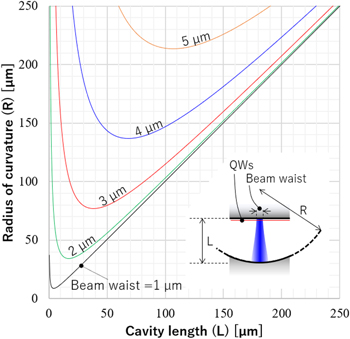
Fig. 9 (Color online) Dependence of beam waist in cavities with plane and curved mirrors on the cavity dimensions. Each line is the calculated relation between cavity length (L) and radius of curvature (R) of the curved mirror for each labeled beam waist, which are equivalent to four times the standard deviation of a Gaussian profile. The inset shows a schematic diagram of the dimension parameters for a cavity. Please see appendix D for more details of the calculations.
Download figure:
Standard image High-resolution imageThe previously published experimental results around this idea with VCSELs are limited. A single precursory work on a similar structure using GaN-based materials was produced by Ref. 48 as early as 2003. They investigated the optical pumping of a GaN-based vertical laser, where 50 μm long cavities with plane and curved end mirrors were used. In that case, InGaN QWs were grown epitaxially on the (0001) plane of a sapphire template, and a curved mirror was fabricated monolithically on the (000–1) plane using ball-up resin patterns as sacrificial masks during RIE of sapphire (see Fig. 10). They reported laser action by observing a clear threshold in an optical output under laser irradiation from a pulsed Nd:YAG laser. The threshold power was 170 kW cm−2 for a wavelength of 355 nm, a pulse width of 5 ns, and repetition at 10 kHz. They observed dense longitudinal mode spacing less than 1 nm, which corresponds to the designed cavity length of 50 μm, and predicted the beam waist was confined within 6 μm by calculation.
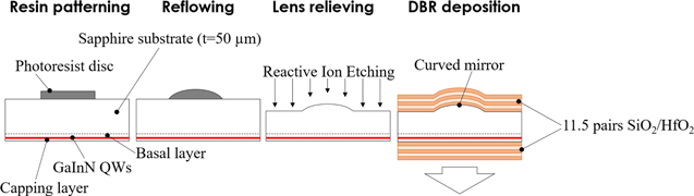
Fig. 10. (Color online) Schematic diagram show the fabrication process for the GaN-based cavity with plane and curved mirrors studied by Ref. 48.
Download figure:
Standard image High-resolution imageThe present authors proposed research to further support and evolve the approach. First, for additional tests with a referential structure, a cavity with two plane mirrors was examined as a worthwhile structure for further confirmation of the potential of the curved mirror. Therefore, it would be valuable to nullify counter-evidence that the sapphire substrate, being transparent to the pumping laser, could allow focus and resonance of pumping photons in a cavity with curved mirrors. Second, the studied structure formed a VCSEL where the cavity medium is occupied by a very thick spacer layer of dissimilar materials compared to those used for the active region. In these structures, the interfaces between semiconductor layers and the thick spacer should be liable to have reflection due to a change in the refractive index and scattering by random structures such as the GaN-buffer layer. All of these structures possibly disturb the resonation; therefore, an attempt was made to eliminate this concern.
The authors' group has conducted further studies with a similar structure, where InGaN wells were grown homoepitaxially on GaN(0001) substrates. GaN is opaque to the pumping laser (349 nm was selected for the study); therefore, there could be no doubt of unintended enhancement in irradiation caused by curved mirrors during the optical pumping test. The cavity with a curved mirror and the referential structure with two plane mirrors, which were both fabricated on the same wafer to strictly confirm whether the curved mirror has a positive effect. After this process, the cavity is filled with a continuous medium of GaN-based materials. Thus, we can omit concerns regarding the interface between semiconductor layers and the thick spacer inside the cavity with an aim to obtain GaN-based VCSELs with low threshold current.
The detailed fabrication procedures of the specimen have been introduced elsewhere.6) Briefly, MOCVD was used to grow four InGaN/GaN QWs, a p-GaN layer doped with Mg (ca. 1 × 1019 cm−3), and a contact layer, to a total thickness of 105 nm on a (0001)-oriented GaN substrate doped with Si (1 × 10¹⁸–19 cm−3). A top-side DBR (11.5 Ta2O5/SiO2 bilayers) was deposited on the contact layer. After lapping the back of the wafer to a thickness of ca. 50 μm, resin disks (diameters from 16 to 80 μm) were patterned on the lapped face of the GaN wafer, i.e., (000–1). The disks were then melted into droplets by heating the specimen to 200 °C. RIE was employed to transfer the surface shape of the resin droplets onto the GaN substrate by removing them as sacrificial masks, which left a lens-shaped surface on the GaN. An n-side DBR (14 Ta2O5/SiO2 bilayers) was deposited there to form the curved mirror. Aside the curved mirror, flat bottom-side mirrors were fabricated as the reference. After those processes, the device structures shown in Fig. 11 were obtained.
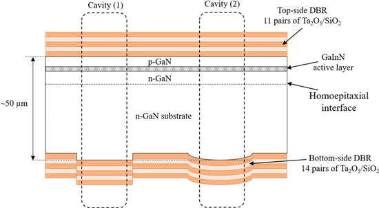
Fig. 11. (Color online) Schematic diagram of the sample used for the optical pumping test to confirm the effect of the curved mirror. In this study two types of cavities were fabricated: cavity (1) with two plane mirrors and cavity (2) with a curved mirror. A comparison was made to investigate the effect of curved mirror incorporation on the cavity behavior.
Download figure:
Standard image High-resolution imageFigures 12(a) and 12(b) show laser confocal microscopy results for a lenslet fabricated on the (000–1) plane of a GaN substrate. The top and bird's-eye views in Fig. 12(a) both reveal the smooth droplet shape formed. In the cross-sectional analysis [Fig. 12(b)], ideal parabolic curves were finely fitted to observed cross-sectional curves. The curvature of the top of the lens is positively correlated with the diameter of the footprint of the lenslets determined by the diameter of the resin disks used for patterning. For example, the radii of curvature were 37.7 and 56.6 μm for resin disks diameters of 40 and 56 μm, respectively.
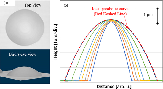
Fig. 12. (Color online) Results of dimension analysis on curve surface formed on (000–1) GaN substrate, where laser scanning confocal microscopy was used. (a) Is top and bird's view observed and (b) is the cross-sectional profile of them. In (b), data for different footprints were overlaid and the red dashed line shown there is an ideal parabolic curve fitted to one of those profiles.
Download figure:
Standard image High-resolution imageFigure 13(a) shows an atomic force microscopy image of the top of the lenslet. The root mean square (RMS) roughness was measured to be 0.2 nm, which is comparable to that reported for a plane mirror that allows laser operation of GaN-VCSEL.38) Figure 13(b) shows a transmission electron microscopy image of the cross-section of the curved mirror of a device. Each DBR layer bends smoothly with the top of the droplets formed on GaN without the introduction of any roughness. Figure 14 shows a reflectivity spectrum for the plane mirror, which provided 99.9%-high reflectivity and a 156 nm wide stopband. Considering the DBR formed on the curved surface has 14 bilayers of the same materials as that shown in Fig. 14, the dielectric DBRs deposited on the curved surface should form a perfect curved mirror.

Fig. 13. (Color online) (a) AFM image of the top of the lens-shaped surface of GaN. The RMS was as low as 0.2 nm. (b) Cross-sectional TEM image of the curved mirror.
Download figure:
Standard image High-resolution image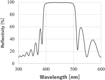
Fig. 14. Reflectivity spectrum for a plane mirror consisting of 11.5 dielectric Ta2O5/SiO2 bilayers measured using a spectrophotometer (Hitachi UH4100). The peak reflectivity was 99.9% and the stopband width was 156 nm at a reflectivity of 50%.
Download figure:
Standard image High-resolution imageFigure 15 shows a cross-sectional scanning electron microscopy (SEM) image of the device used for optical pumping tests. The cavity length of the specimen was measured to be 49.8 μm in this case. Note that there was no interface between the MOCVD-grown n-type GaN and the GaN substrate. In the previous research on similar structures, the cavity possesses an interface between two different cavity media, which is considered to be an obstacle for resonation.
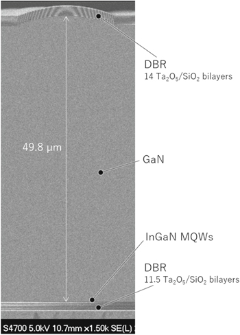
Fig. 15. Cross-sectional SEM image of the device. The cavity length (the distance between the top of the curved surface and the plane surface of GaN) was measured to be 49.8 μm.
Download figure:
Standard image High-resolution imageLasing tests were conducted by optical pumping with the following conditions. The excitation source was pulsed at 349 nm (pulse width: <5 ns, frequency: 1 kHz, beam diameter: 200 μm, Spectra Physics Explorer) and injected at 45° to the sample. The optical output of the device was measured by the peak power obtained through a spectrometer (Ocean Optics USB4000) via an optical fiber. A CCD camera was used intermittently to observe the sample via a half mirror.
Figures 16(a) through 16(d) show the results of the tests. A clear threshold at a pumping power of 0.2 mW in the input–output curves [Fig. 16(a)] was observed for the cavity with curved mirrors. The results with this cavity also showed narrowing in the emission spectrum [Fig. 16(b)] and bright spots in the CCD image [Fig. 16(c)]. In contrast, the cavity with two plane mirrors showed no threshold, a broad spectrum, and a darker spot. These results indicate that the curved mirror improves the quality of the cavity over that with only the plane mirrors, and that incorporation of a curved mirror enables laser action, even at long cavity lengths up to 49.8 μm.
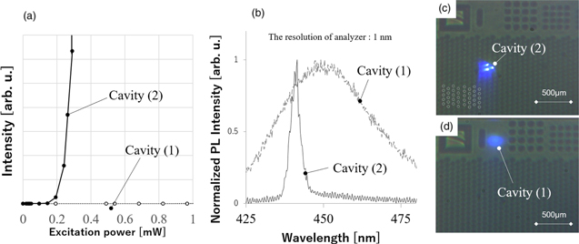
Fig. 16. (Color online) Results of the optical pumping test. (a) Input–output curves for the devices. (b) Photoluminescence (PL) spectra for the devices under a pumping power of 0.3 mW. Visual images of specimens under optical pumping for (c) cavity (2) clad with curved and plane mirrors, and (d) cavity (1) with two plane mirrors, respectively.
Download figure:
Standard image High-resolution imageFigure 16(b) shows that a cavity with a curved mirror gives an emission spectrum with a full width at half maximum of 3.2 nm at a pumping power of 0.3 mW. The resolution limit of the spectrometer, 1 nm, is greater than the longitudinal mode spacing of 0.7 nm, calculated for the cavity length of 49.8 μm. The low resolution of the spectrometer causes the spectrum to have an envelope over multiple longitudinal modes.
To conclude, an ideal curved mirror can be formed on GaN(000–1) with an RMS of 0.2 nm using re-flown photoresist lenslets as sacrificial etching masks. It was confirmed that these curved mirrors have a positive effect to improve cavity quality compared to that for conventional cavities with flat mirrors. Cross-sectional analysis did not reveal a homoepitaxial interface, which should be advantageous in reducing the threshold current for GaN-based VCSELs with this structure. Although this study provided no direct evidence to support the occurrence of lateral optical confinement, the laser action in such a long cavity implies the optical guiding effect was realized within the proposed structure as theoretically predicted.47) The validity of this opinion is investigated later in Sect. 6.
5. Lateral current confinement by BII
Lateral current confinement is another important factor to enable efficient laser operation of VCSELs with low threshold current. As stated in Sect. 3, there was a report that aperture formation using aluminum-ion implantation is effective to reduce the threshold current.41) However, there has been no published research that has fully examined aperture formation of BII as having a positive or negative effect on the characteristics of GaN-based VCSELs. Therefore, the authors investigated the fundamental contribution of implanted boron to GaN-based VCSELs by assessing the increase in the optical absorption of GaN and the reduction of luminance of an LED device due to BII.
The detailed experimental procedures have been given elsewhere.4) Here brief comments are given. First, secondary ion mass spectroscopy (SIMS) was used to evaluate GaN-substrates after BII. Figure 17 show the depth profile of boron in a specimen. The boron atom concentration near the wafer surface was 3 × 1019 cm−3 and decreased exponentially with the depth.
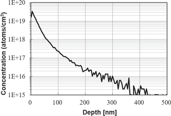
Fig. 17. Boron depth profile in GaN as measured using SIMS. The surface of the specimen is located at a depth of 0 nm. The active region of a GaN-based VCSEL is commonly placed around a depth of 100 nm.
Download figure:
Standard image High-resolution imageThe optical parameters were observed for this specimen and for a bare GaN substrate without implantation as a reference using ellipsometry (see Fig. 18). BII caused a slight increase in the refractive index of GaN, and it dulled the absorption edge of GaN, giving an absorption of less than 2000 cm−1 in the potential lasing wavelength range for visible GaN-based VCSELs, i.e., 400–550 nm. The 400 μm thickness of the GaN wafers is greater than the coherence length of the light sources used for the ellipsometry measurement system (several micrometers for J. A. Woollam M-2000VI); therefore, ellipsometry gives the optical parameters for almost the entire surface. It is assumed that the increase in the absorption and refractive index caused by BII would be proportional to the boron concentration in GaN obtained by SIMS. Therefore, an estimation could be given where increases in those parameters caused by BII have peaks at the surface of GaN and tails with depth. The peak values for absorption and reflective index at the surface were 800 cm−1 and 0.06, for example at 450 nm.
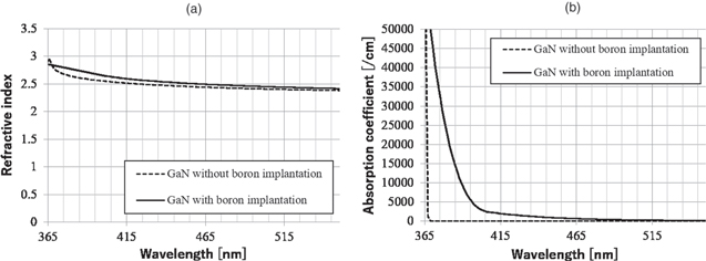
Fig. 18. Optical parameters obtained for specimens using ellipsometry. (a) Refractive indices and (b) absorption coefficients as a function of wavelength.
Download figure:
Standard image High-resolution imageIt is argued how these shifts in the optical parameters impact on the characteristics of GaN-based VCSELs. Assuming that the shifts affect a GaN-VCSEL, vertical profiles of refractive index and absorption coefficient are shown in Fig. 19. The simulated electric field in the device was overlaid on those profiles. On the basis of these results, BII causes absorption of 0.42% per round trip in the cavity if a photon travels in a region where boron is fully implanted. If the cavity mode is fully included by the aperture in the lateral direction, then this value can be zero. If not, then slight tailing of the optical field into the implanted area causes only an insubstantial absorption. The value was estimated to be much less than 0.1%, by considering possible beam profiles.4) The change in refractive index corresponds to a 2.2 nm extension in the effective length of the cavity, which is small with respect to the targeted cavity length (>20 μm), offering 0.01% shift in resonant wavelengths. Although extension at the outer side of the cavity gives an anti-guiding effect, as concave structures do, numerical simulation indicated that this value causes only a negligible loss.39,40)
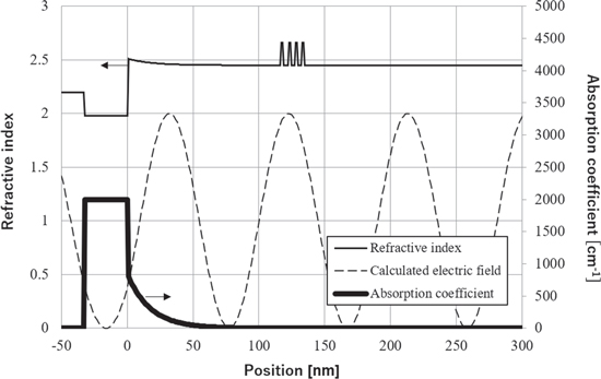
Fig. 19. Vertical profiles of refractive index, absorption coefficient, and electric field in the resonance mode, as discussed in this study. The horizontal axis represents the position in the vertical direction of the GaN-VCSEL, where the interface between ITO and p-GaN is set at zero. The thin solid line is the refractive index profile. The dashed line is calculated electric field (E2) in the resonance mode. The bold solid line is the absorption coefficient. Here, an absorption coefficient of 2000 cm−1 was adopted for ITO.49)
Download figure:
Standard image High-resolution imageApart from optical parameters, the electrical effects caused by BII were experimentally studied by observing the dependence of the luminance on the current apertures. The structure of the GaN-based LED used to this experiment is shown in Fig. 20(a). The epistructure was the same as that used in the former section. Boron ions were implanted into all areas of the specimen except for the circular (diameters: 6, 8, 10, and 15 μm) current injection regions, which were masked to avoid implantation and obtain lateral electrical confinement. A 30 nm thick ITO layer was deposited on the contact layer. A Ti/Pt/Au n-electrode was deposited both on a part of the ITO and the bottom of the substrate. The brightness in the vertical direction was observed under CW current injection [see Fig. 20(b) for the details of the measurement setup].
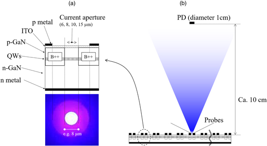
Fig. 20. (Color online) (a) Schematic diagram of the LED sample used for this experiment and an NFP of an LED sample with an aperture size of 8 μm measured at 30 mA,37) where the spot size of the light emitting region was observed to be 8 μm. (b) Schematic diagram of the setup used for the measurement. This indicates that implanted boron blocks current injection into the active region and defines the current aperture.
Download figure:
Standard image High-resolution imageThe current density–luminance output (J–L) curves measured for LED samples are shown in Figs. 21. For both axes, values are normalized with respect to the current injected area of each device. The slopes of each curve represent the efficiency of the samples. The J–L curves did not show a clear dependence on current aperture size at current densities of up to 30 kA cm−2; therefore, implanted boron does not have a negative effect on carrier injection when the current aperture diameter is between 6 and 15 μm. Assuming current flow does not differ between LEDs and VCSELs for the studied structures, carrier loss caused by BII should not be serious in VCSELs as well.
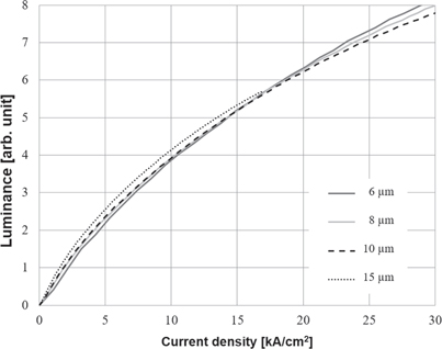
Fig. 21. Luminance-current density curves observed for four types of LED emitters with different apertures (6, 8, 10, and 15 μm).
Download figure:
Standard image High-resolution imageWe were interested on whether non-radiative recombination centers generated by BII have a negative effect. As stated in the former section, the active region of the fabricated GaN-VCSEL was located at a depth of approximately 100 nm, which indicates that boron ions should penetrate the active region when applied to these structures (see Fig. 18). This implies that numbers of recombination centers will be formed in, above, and beneath the QWs when using this approach, which should perturb the lattice to form defects that serve as non-radiative recombination centers.50) However, the J–L curves of the LED samples showed no aperture size dependence, which indicates that the non-radiative recombination due to BII is not dominant. This discrepancy suggests an interesting insight, in that the diffusion length of carriers in InGaN QWs is smaller than the range of aperture sizes adopted in this study. This is in agreement with previous reports of submicrometer diffusion lengths in InGaN layers.51,52) The diffusion length of carriers in QWs in GaAs-based materials used for conventional VCSELs is ca. 2–3 μm,53) which reduces the efficiency of VCSEL operation when the apertures are smaller than those diffusion lengths.54) This difference is due to the nature of the material systems. InGaN tends to experience a separation into In-rich and Ga-rich phases,55) while InGaAs has complete solid solubility above room temperature to form a homogeneous distribution.56) This is a very important point in research on the miniaturization of GaN-based VCSELs. Granted that the carrier diffusion length limits the lower limit of an aperture diameter in a VCSEL, further miniaturization of the aperture in GaN-based VCSELs with InGaN QWs could be expected using BII.
6. GaN-based VCSELs operated by current injection
This section reviews the current-driven operation of GaN-based VCSELs with the proposed structure; equipped with a curved mirror made of dielectric materials, a cavity longer than 20 μm, and a lateral confinement structure using BII [a schematic of the structure is given in Fig. 1(a)]. Through Sect. 4, cavities with the former two features, a curved dielectric mirror and a long cavity, were confirmed to form GaN-based VCSELs that were better than those with two plane mirrors. Section 5 gave results illustrating that BII provides efficient lateral current confinement down to a small aperture diameter of 6 μm with negligible increase in the optical and carrier loss. This section introduces the laser operation of GaN-based VCSELs, where these structures are combined into each single emitter under current injection. The optical pumping test study shown in Sect. 4 did not provide certain evidence of lateral optical confinement. Therefore, here we investigate near-field patterns of the device.
The detailed fabrication process have been reported previously,6) and is almost a combination of the processes used for the experiments detailed in Sects. 4 and 5. Among the current aperture diameters of 6–15 μm as introduced in Sect. 5, this study investigates two smaller apertures of 6 and 8 μm, with an aim to miniaturize GaN-based VCSELs. Furthermore, the cavity structure parameters L and R are set to be 20–30 μm and 60–80 μm, respectively, to keep the beam waist of the cavity mode less than 3 μm, which is sufficiently less than the current aperture diameter of 6 μm so that the current aperture will fully include the cavity mode in the lateral direction.
Measurements of I–L, output spectra and near-field imaging under pulsed current injection were conducted with the device illustrated in Fig. 1(a). Figure 21(a) shows the I–L curves obtained for two devices with different aperture sizes (6 and 8 μm) fabricated on the same substrate. The threshold currents were 40 and 70 mA for the devices with aperture sizes of 6 and 8 μm, giving Jth values of 139 and 141 kA cm−2, respectively. The Jth values were almost the same, despite the difference in the aperture size. This is a significant result when considering the lateral optical behavior of the cavity modes. If it were not for waveguiding, shrinkage of the beam waist from 8 to 6 μm for a long cavity between 20 and 30 μm would occur, which would generate diffraction losses greater than 1% per round trip. This value exceeds the typical estimated gain for GaN-based VCSELs (see Fig. 7). Considering that the gain of active region suffers from saturation under carrier injection, this shrinkage should have induced a considerable increase of Jth without any waveguiding structures inside the cavity. Therefore, the stability of Jth provides one piece of evidence of lateral optical confinement in these structures. Note that the previously reported GaN-based VCSELs have an increasing trend toward smaller apertures of approximately 6–8 μm, even though they had short cavities of less than several micrometers (see Fig. 8). Thus, the independence of Jth with respect to the aperture size for this long cavity is quite significant. Figure 22(b) shows an emission spectrum observed below and above the threshold current for a typical sample with a 6 μm diameter aperture. This clearly shows the behavior where a few modes were enhanced above the threshold current and illustrates the occurrence of laser operation. Each peak is associated with weaker satellite peaks, which seem to originate from other longitudinal and higher-order transverse modes. The mode spacing of 1.27 nm shown in Fig. 22(b) corresponds to a cavity length of 28.3 μm for the following parameters: n = 2.45, λ = 454 nm, and dn/dλ = −0.001.
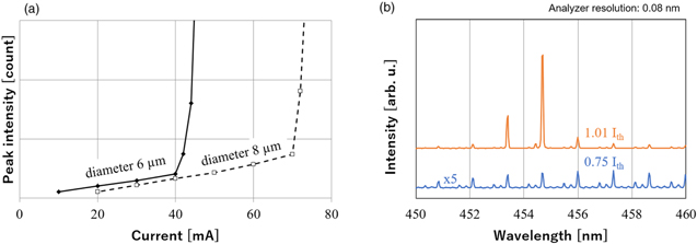
Fig. 22. (Color online) I–L curves obtained for devices with an aperture size of 6 and 8 μm and (b) spectrum around the threshold current for a typical sample with a 6 μm aperture.
Download figure:
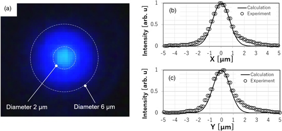
Standard image High-resolution imageDimensional analysis, cross-sectional SEM and laser scanning confocal microscopy revealed that the cavity length and curvature of the mirror were 28 and 74 μm, respectively (data not shown), which give a theoretical beam waist of 2.8 μm (see Fig. 9). To confirm the lateral optical confinement with the curved mirror, NFP was observed. Figure 23 shows the result of NFP analysis performed on a device with a 6 μm diameter aperture. In Fig. 23(a), the NFP image of this device has a small bright spot in the center of the current aperture. In Figs. 23(b) and 23(c), the cross-sectional near-field profiles illustrate the experimental NFP fits to the theoretically predicted value of 2.8 μm. This result directly indicates the occurrence of lateral optical confinement with the curved mirror, and the beam waist is determined by the cavity length and curvature of the mirror.
Fig. 23. (Color online) (a) NFP imaging. (b), (c) Cross-sectional profiles of NFP in both directions. The solid lines in (b) and (c) are the theoretical curves obtained through measured dimension parameters (L and R) through laser confocal microscopy and cross-sectional SEM imaging.
Download figure:
Standard image High-resolution image
The cavity mode with such a small beam waist suffers a diffraction loss close to 100% per round trip (see Fig. 7). Thus, the result of laser operation is the most powerful evidence for this effect.
It is problematic that the threshold current density was as high as 140 kA cm−2 and the aperture was still larger than some previously reported cases. This resulted in a high threshold current of 40 mA for pulsed current injection. As introduced in Sect. 3, the lowest threshold current density is 1.2 kA cm−2 34) and the lowest threshold current of approximately 0.5–0.6 mA was reported for the smallest current aperture of 3 μm44) for a GaN-based VCSEL under CW operation. Thus, further improvement of this device is required to lower the threshold current with this structure.
7. Contemporary and future work
The series of studies in Sects 4, 5, and 6 revealed significant insights into the fundamental aspects of GaN-VCSELs. The implementation of lateral optical confinement using a curved mirror can nullify diffraction loss, and it is expected that appropriate setting of the cavity dimensions can shrink the beam waist (e.g., 3 μm). BII allows for a flat configuration and small aperture (e.g., 6 μm), mostly without optical loss or carrier loss. These results have motivated us toward further improvement of the cavity quality and miniaturization of GaN-VCSELs with the proposed structure to achieve a low threshold current.
This section gives the latest progress of the authors' research on GaN-based VCSELs with the proposed structure. After reviewing such, ideas on future research regarding this unique structure will be given with respect to other contemporary research and potential applications. Please note that the latest results of the authors have only ever appeared in previous oral presentations. These results are mostly planned to be published as independent articles; however, as a progress review prepared for this IWN2018 special issue, concise summaries of these works are given here.
First, the independence of Jth with respect to the aperture diameter down to 4 μm was confirmed.7) The controllability of NFP with variation of the cavity dimension was also confirmed by observing multiple devices.7) Based on these results, further improvements were attempted and three main topics, lowering of the threshold current, enhanced output, and high yield, were reported in the last IWN2018.9) Further miniaturized devices were fabricated, where an aperture diameter of 3 μm and a beam waist of 1.3 μm were adopted. The structure of this device was achieved with minor modifications, such as a reduction in the ITO layer thickness (30–20 nm) and a change in the number of QWs (four to three), both of which were intended to suppress internal loss and enhance gain.57) This device gave the following results under CW operation at room temperature: Ith = 0.25 mA, Jth = 3.5 kA cm−2, peak output power (Pmax) of 0.3 mW at 5 mA, and a wavelength of 445.3 nm (see Fig. 24).10) This is the lowest recorded threshold current reported for a GaN-based VCSEL at the present time.
Improvement in the output power was also achieved. The number of Ta2O5/SiO2 DBR pairs on the front mirror was reduced from 11.5 to 7.5 (corresponding to a 99.9%–99.3% reduction in reflectivity) to improve SE. The aperture diameter was enlarged to 8 μm. The modified device showed the following characteristics: Ith of 3.8 mA, Jth of 7.6 kA cm−2, Pmax of 11.8 mW at 25 mA, an SE of 0.83 W A−1 and a peak WPE of 9.5%. This is comparable to a single previous example where an output higher than 10 mW was achieved, as reported by Refs. 46 (Pmax = 15.8 mW, SE = 0.85 W A−1, peak WPE = 8.9%), where a nitride semiconductor DBR was used.58)
Other than those, the lasing yield of the devices was reported.9) The lasing behavior of 144 emitters spread over a 10 × 25 mm sample wafer was investigated, and the following results were obtained: number of lasing emitters of 144 out of 144, and the standard deviation of the threshold current was 10% of the average. To the best of our knowledge, this is the first example of the lasing yield being reported.
Now we consider future work with the proposed structure. First, there should be room for further research toward enabling smaller apertures. There remains a gap between the current aperture (3 μm) and beam waist (1.3 μm) confined by a curved mirror in the device that showed the lowest threshold current of 0.25 mA.10) Therefore, it would be worthwhile to fabricate devices with apertures smaller than 3 μm. Miniaturization of beam waist settings L and R should facilitate further reduction in the aperture diameter. Those factors that limit aperture size reduction are (i) degradation of the injection efficiency due to non-radiative recombination associated with BII, (ii) the focusing ability of the curved mirror, and (iii) the positioning accuracy in lateral direction between curved mirrors and current apertures. Factor (i) was discussed in Sect. 5. Further investigation toward apertures smaller than a few micrometers will be worthwhile. With regard to factor (ii), classical optics theory59) predicts the minimum of focused light is defined as the diffraction limit, which is reciprocal to the numerical aperture (NA) of a curved mirror. Assuming the entire area of a convex surface contributes as an ideal curved mirror, the effective NA of those appeared in Sect. 4 are approximately 0.7, which enables the beam waist to be focused around at the lasing wavelength. Such small structures demand factor (iii), a higher positioning accuracy of curved mirror to the current aperture in the lateral direction, for the cavity modes to hit the active region.
Efficiency should also receive significant attention. The WPE of GaN-based VCSELs has been as low as 1%. However, recent progress has boosted the WPE to close to 10%,9,46) which has encouraged researchers on GaN-based VCSELs to further improve the efficiency. Considering the WPE values of InGaN-based EELs are reaching 40%, this value should be a threshold for GaN-based VCSELs to replace classis EELs and some high brightness LEDs in practical use nowadays. To achieve this, further investigation to quantitatively clarify the internal loss and gain behavior of the proposed devices is required.
Arraying will be the next topic of GaN-based VCSELs. The word "array" has often been used in papers on this device, especially in the introduction sections. However, experimental data on arrayed GaN-based VCSELs under operation are absent. This is seemingly due to difficulty in the fabrication of GaN-based VCSELs, as discussed in Sect. 3. The proposed structure possesses high lasing yield with a stable threshold current distribution. Arraying hundreds of emitters with higher optical output above 10 mW will enable super-watt-class GaN-based VCSEL arrays in the near future. In the proposed structure, the arraying pitch is limited by the footprint of the curved mirrors. For example, lenslets diameters between 40 and 56 μm appeared in Sect. 4. Reduction of these values will be the key toward shrinkage of the die size, which would improve both fabrication costs and etendue of the device. Such advantages would help arrayed blue GaN-based VCSELs compete with watt-class blue EELs used for applications such as car head lamps. Arraying LEDs in a matrix is used as an approach to enable beam steering of car head lamps. GaN-based blue VCSELs both with arraying ability and strong directionality could be superior to LEDs in this application.
The arraying of these devices should arouse attention on the heat management of the devices more than before. The literature indicates that an increase in the thickness of GaN is effective to improve the thermal resistance of the device.60–62) This extension of highly thermal conductive GaN63,64) facilitates heat dissipation from the active region. Reference 46 reported improvement in the thermal resistance of GaN-based VCSELs from 1100 to 710 K W−1 by extending the cavity mainly filled with GaN from 5 to 10λ, beside where an AlInN-based DBR with low thermal conductivity65,66) blocked heat dissipation. Such proposed devices, which would already have cavities longer than 100λ, would be significantly advantageous to the pursuit of high thermal conductivity in the devices.
On the other hand, such long cavities have negative associations. In the proposed devices, the main part of the cavity being filled with n-GaN originated from a Si-doped GaN substrate used for fabrication. Reference 67 reported that the optical absorption of Si-doped GaN is proportional to its doping level, where 0.4–3.9 cm−1 were shown for the doping level of GaN substrate used for the studies stated in Sects. 4–6 (Si ca. 1 × E18-19). Thus, a thick n-GaN filling cavity potentially provides optical loss in a range between 0.2% and a few percent. Control of the doping level in the substrate is thus essential to stabilize the internal losses of the proposed structure. Such a long cavity induces multi-longitudinal mode operation of the device, as shown in Fig. 23(b), and limits the operation frequency. This could reduce the advantages of VCSELs for such applications as optical coherence tomography and optical communications. The proposed structure may not be suitable for those applications as it is.
Application of semi-polar plane substrates for GaN-based VCSELs with this structure would assist fabrication of a green VCSEL. There is limited literature on green emission from GaN-based VCSELs. According to previous reports, it is difficult to achieve CW lasing at green wavelengths for GaN-VCSELs on conventional c-plane GaN substrates,32) due to the strong piezoelectric fields of the InGaN QWs. On the other hand, semi-polar {20–21} GaN substrates, which have weaker piezoelectric fields compared to c-plane GaN substrates, suppress the increase of the threshold current in the green wavelength region.68–71) For example, Murayama reported high-efficiency green laser diodes fabricated on free-standing semi-polar {20–21} GaN substrates,71) and utilization of the {20–21} plane seems to be suitable for green VCSELs. However, most CW-operable GaN-VCSELs reported to date were fabricated on c-plane GaN substrates, and their lasing wavelengths were mostly limited to a range of blue-violet to blue. The proposed structure discussed in this review has potential for use with {20–21} GaN substrates to enable green emission without a problematic increase in the threshold current. The realization of green VCSELs would enable full color displays that use RGB-VCSELs as light sources. The small power consumption of such light sources would be suitable for mobile displays. Moreover, the use of semi-polar plane GaN substrates would be profitable for control of the polarization directions.72)
8. Conclusions
This progress review has introduced previous research of the authors regarding the development of GaN-based VCSELs with features such as an extremely long cavity, as long as 20 μm or more, plane and curved reflectors, DBRs made of dielectric materials, and BII used to form current apertures.4–10) In this device, the size of the beam waist is defined by the cavity length and radius of curvature of the curved mirrors. By setting these dimensions, the lateral mode is confined to as small as 1.3 μm, which enables a low threshold current (Ith = 0.25 mA) for a small aperture diameter of 3 μm. The lateral optical confinement nullified diffraction loss due to long cavity and enabled high output power (up to 11.8 mW) with high efficiency (WPE = 9.5%). The adoption of dialectic mirrors and such a long cavity enabled a robust fabrication process to give very high lasing yields (100% for 144 emitters on a single wafer) with a stabilized threshold current (σ = 10%). These results indicate that this type of GaN-based VCSEL is expected to realize novel devices, such as watt-class arrayed GaN-based VCSELs and green VCSELs in the future.
Acknowledgments
The authors are grateful to the following colleagues who have worked on the development of GaN-based VCSELs at the Sony Corporation: Mr. Mitomo, Mr. Satou, Mr. Fujii, Mr. Watanabe, Mr. Jyoukawa, Mr. Ito, Ms. Kobayashi, Ms. Ohara, Mr. Kawanishi, Mr. Futagawa, Dr. Koda, Dr. Narui, and Dr. Yanashima. The authors thank Dr. Kishino and Dr. Kikuchi of Sophia University, Dr. Kuramoto of Stanley Electronics, and Dr. Takeuchi of Meijo University for helpful advice during the writing of this paper. The authors thank Dr. Kawakami and Dr. Funato of the University of Kyoto for their encouragement with this study. The authors thank all the committee of IWN for their dedication to that conference.
Appendices
Appendix A.: VCSEL amplification rate per round trip
For this calculation, a simple formula is used:

where r is the VCSEL amplification rate per round trip, Г is the enhancement factor, and t and g are the total effective thickness and material gain of active layer, respectively. In VCSELs, QWs are often used as the active region; therefore, assume the same in this review. Г is the ratio of the average optical power over QWs and the average for the entire cavity. In VCSELs, QWs are usually designed to be at the antinode of the resonant mode. Thus, Г can be approximated as 2.
Appendix B.: DBRs and refractive index difference
In this review, the stopband width and peak reflectivity of a DBR are calculated using the following formula:73)

where Δλstopband is the width of the DBR stopband, and λ0 is the quadruple of the light path equivalent to the thickness of each layer of DBRs, commonly designed to be the lasing wavelength of the device. nH and nL are the refractive indices of the materials used for the DBRs (nH > nL).
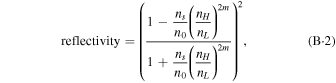
where nS and n0 are the refractive indices of the materials that comprise the front and back of the DBR mirror, and m is the number of pairs used for the DBR. In this calculation, the ratio of nS to n0 is set to be one. The calculations in this review were performed for assumed nH/nL values of 1.22 for AlAs/GaAs, 1.07 for Al0.8In0.18N/GaN, 1.14 for AlN/GaN, 1.34 for SiN/SiO2, and 1.48 for Ta2O5/SiO2.
Appendix C.: Formulation for diffraction loss, aperture diameter and cavity length
The detailed background for the calculation has been given elsewhere.6) Here, only the result of the formulation is given:
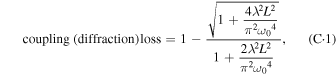
where λ is the lasing wavelength, L is the cavity length and ω0 is the beam waist radius of the initial Gaussian beam. In the simulation shown in Fig. 6, the current aperture diameter is equivalent to two times ω0. This assumption sets up the situation where the beam waist expands to as large as the current aperture.
Appendix D.: Beam waist formed in a cavity with plane and curved mirrors
An analytical formulation describing the waist size of a Gaussian beam was given by Ref. 47:
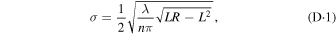
where σ is the standard deviation of the Gaussian profile, n is the equivalent refractive index of the cavity medium, L is the cavity length, and R is the radius of curvature of the curved mirror. Thus, this formula predicts the beam waist can be controlled by L and R of a cavity. n = 2.45 and λ = 2.45 nm are assumed for the calculation in this paper. The beam waist diameter is assumed to be 4σ throughout this paper.
Biographies

Tatsushi HAMAGUCHI was born in Osaka, Japan in 1980. He received the B.S. and M.S. degrees in material science and engineering from Kyoto University in 2004 and 2006. He received the Ph.D. degree in electronic engineering from Sophia University in 2019. From 2006 to 2008, he worked at the Nitride Semiconductor Research Laboratory of Nichia Corporation. After 2008, he worked for Sony corporation, where he did development of nitride-based edge-emitting lasers and vertical-cavity surface-emitting lasers (VCSELs). He has acted as the leader of the Sony's project team for nitride-based VCSELs during the recent years.

Masayuki TANAKA was born in Yokohama, Japan in 1979. He received the B.S. and M.S. in chemical engineering from Yokohama National University in 2004 and 2007, respectively. From 2009 to 2012, he served as the production engineer for multiple projects aiming mass production of light emitting devices at Sony corporation. After 2013, he worked for researching division, serving as the process engineer of the Sony's project team for nitride-based VCSELs.

Hiroshi NAKAJIMA was born in Nagano, Japan in 1970. He received the B.S. and M.S. degrees in material science and engineering from Waseda University in 1994 and 1996, respectively. In 1996, he joined Sony corporation. Since then, he has engaged in research and development on several types of semiconductor lasers, and is currently working at Sony's project team for nitride-based VCSELs.