

Abstract
We present a vertical GaN planar metal-oxide-semiconductor field-effect transistor (MOSFET) fabricated by an all ion implantation process. The fabricated MOSFET shows an on-resistance of 2.78 mΩ cm2 and a breakdown voltage of 1200 V, by applying the short cell pitch design to reduce the on-resistance and a Mg and N sequential implantation to improve the breakdown voltage of the pn-junction. By evaluating each on-resistance component in the fabricated vertical GaN planar MOSFET using the simultaneously formed test structures, an effective on-resistance of the active region excluding the source parasitic resistance is 1.4 mΩ cm2. Consequently, it was demonstrated that an all ion implantation process can fabricate a vertical GaN planar MOSFET with a high breakdown voltage and low on-resistance. This result will greatly contribute to the realization of GaN power devices.
Export citation and abstract BibTeX RIS
1. Introduction
Gallium Nitride (GaN) has attracted attention as a semiconductor material for next-generation power switching devices. Vertical-type GaN devices with metal-oxide-semiconductor (MOS) gate driving are preferable for high-power switching applications. Due to recent advances in bulk GaN crystal growth,1) more studies are reporting vertical-type GaN devices with a breakdown voltage exceeding 1 kV on GaN substrates.2–12) However, all these reports use an epitaxially grown p-type layer.
For practicality and reliability viewpoints, it is essential to form a p-type layer by ion-implantation (I/I). Ion implantation requires a high-temperature activation heat treatment, however, heat treatment at 800 °C or higher decomposes GaN due to the very strong triple bond of N molecule that reduces the negative Gibbs free energy of the nitride component.13,14) Consequently, p-type formation by ion implantation into GaN is extremely difficult.
The p-type characteristics of Mg implanted layer have been reported recently. For example, the photoluminescence (PL) spectrum shows that some of the implanted Mg atoms form acceptors because the observed acceptor-related UV luminescence is similar to that of epitaxially grown p-GaN layers.15) The rectification property of the pn junction and the electroluminescence (EL) emission have also been confirmed.16,17) Sakurai et al. demonstrated p-type hole conduction in the Mg-implanted GaN layer annealed at 1400 °C under a nitrogen pressure of 1 GPa using the temperature dependence of the Hall effect.18) In addition, we reported MOS field-effect transistor (MOSFET) operations on the Mg ion implanted layer and the correlation between the MOS channel properties and Mg ion implantation dose.19,20) Other recent reports have improved the characteristics of the Mg implanted layer by sequential implantation of Mg and H or N.17,21) We also evaluated the subsequent H or N implantation effect on the electrical characteristics and defects in the ion implanted region. Subsequent H implantation introduces more hole traps in p-GaN, while N implantation suppresses these hole traps.22)
To demonstrate the characteristics of GaN devices, we previously reported the normal operation of the first vertical GaN planar MOSFET fabricated by an all ion implantation process.23) However, the on-resistance was as large as 10 mΩ cm2, while the breakdown voltage was as low as 300 V. The large on-resistance was attributed to the considerable design cell pitch, while the low breakdown voltage was due to the low activation ratio of the Mg implanted layer. Hence, we demonstrated a vertical GaN planar MOSFET with a high breakdown and low on-resistance fabricated by an all ion implantation process in SSDM2019.24) Specifically, we applied Mg and N sequential implantation to improve the breakdown voltage of the pn-junction and a short cell pitch design to reduce the on-resistance. Herein we demonstrate that an all ion implantation process can fabricate a vertical GaN planar MOSFET with a high breakdown and low on-resistance. We provide detailed data about the improvement of the pn-junction breakdown voltage due to N sequential implantation and evaluate the on-resistance component.
2. Experimental methods
2.1. Fabrication of a Mg and N sequentially implanted pn-diode
To evaluate the pn-junction breakdown voltage, we fabricated a pn-diode by ion implantation. Figure 1 schematically depicts the fabricated pn-diode. The n-type GaN (0001) substrate was obtained by hydride vapor phase epitaxy. Then a 10 μm thick n-GaN layer was epitaxially grown by metal organic chemical vapor deposition (MOCVD) on the substrate. The net donor concentration of the n-GaN epitaxial layer was around 1.5 × 1016 cm−3. Mg ions were selectively implanted on the n-GaN layer. The Mg ions were implanted with 10–240 keV and a total dose of 8.4 × 1013 cm−2 to obtain a 0.3 μm thick box-profile of 1 × 1018 cm−3 with a p+ contact layer of 2 × 1019 cm−3 near the surface. After Mg ion implantation, N ion implantation was carried out sequentially. N ions were implanted with 10–180 keV and a total dose of 9.9 × 1013 cm−2. In addition, samples without N sequential implantation were fabricated.
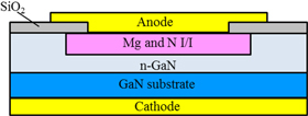
Fig. 1. (Color online) Schematic of the cross section of the fabricated GaN pn-diodes.
Download figure:
Standard image High-resolution imageAfter Mg and N implantation, the wafers were annealed at 1300 °C for 5 min in a N2 atmosphere at standard pressure with an AlN encapsulation cap to prevent GaN dissociation. After annealing, the AlN cap was chemically removed. AFM measurements in a 1 μm square area indicated that the typical root-mean-square surface roughness of GaN after activation annealing was 0.25 nm.
A plasma-CVD apparatus with TEOS gas deposited a 400 nm thick SiO2 layer for the field insulating film at 350 °C. The anode was composed of nickel and gold, while the cathode was composed of titanium and aluminum.
Figure 2 shows the depth profile of the Mg concentration analyzed by SIMS for each sample before and after activation annealing. The Mg profile before annealing between the Mg implanted layer and the Mg and N sequential implanted layer were the same. However, the Mg profile after annealing differed slightly at a depth of about 100 nm.
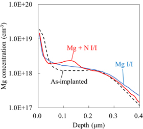
Fig. 2. (Color online) Depth profile of the Mg concentration of the fabricated pn-diodes analyzed by SIMS measurements.
Download figure:
Standard image High-resolution image2.2. Fabrication of a vertical GaN planar MOSFET
Figure 3 schematically depicts the fabricated vertical GaN planar MOSFETs by the all ion implantation process. A short cell pitch design of 5 μm with an i-line stepper was used to reduce the channel resistance. The designed size of the active region on the photomask was 91 μm × 40 μm. The designed channel length (Lch) was 1 μm. The junction FET (JFET) length (LJFET) was 1 μm, and the source length (Lc) was 2 μm. In consideration of the current spread in the drift layer, the area of the active region used to calculate the on-resistance was set to 101 μm × 50 μm by adding the drift layer thickness (10 μm) to the designed size of the active region assuming a 45° model.25)
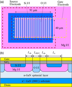
Fig. 3. (Color online) Schematics of the fabricated vertical GaN planar MOSFETs. (a) Plan view without a SiO2 layer and (b) cross sectional image of the active region.
Download figure:
Standard image High-resolution imageWe adopted a single-layer electrode structure to avoid the complicated process of stacked electrodes [Fig. 3(a)]. The source parasitic resistance of a single-layer electrode structure was large compared to the stacked electrode in vertical contact with the source implanted region because the source electrode of a single-layer electrode structure is in contact with the active region at a position besides the horizontal direction. The sheet resistance in the source implanted region was about 100 Ω sq−1, and 18 source implanted regions measuring 2 μm width and 40 μm length were connected in parallel in the active region. Considering the horizontal current flow, the estimated source parasitic resistance was 1.4 mΩ cm2. Since the source parasitic resistance was considered to be very large relative to the on-resistance of the vertical GaN MOSFET, the source parasitic resistance must be measured and subtracted from the on-resistance to evaluate the effective on-resistance of the active region.
The n-type GaN (0001) substrate was obtained by the acidic ammonothermal method. Then a 10 μm thick n-GaN layer was epitaxially grown by MOCVD on the substrate. The net donor concentration of the n-GaN epitaxial layer was around 1 × 1016 cm−3.
Firstly, Mg ions were selectively implanted on the n-GaN layer. Mg ions were implanted with 10 to 700 keV with a total dose of 6.5 × 1013 cm−2. Afterwards, N ions were implanted sequentially with 10–600 keV and a total dose of 6.7 × 1013 cm−2. Secondly, Si ions were selectively implanted into the source regions with 15–40 keV and a total dose of 1.9 × 1015 cm−2. Thirdly, O ions were selectively implanted into the JFET region with 10 to 700 keV and a total dose of 2.3 × 1013 cm−2 to reduce the JFET resistance.
After the triple ion implantation, the wafers were annealed at 1300 °C for 5 min in a N2 atmosphere at standard pressure with AlN encapsulation cap. Finally, the AlN cap was chemically removed.
Then a plasma-CVD apparatus with TEOS gas deposited a 100 nm thick SiO2 layer at 300 °C. Titanium and aluminum were used as the gate, source, and drain metal, while nickel was used as the body contact metal. Forming gas annealing was performed at 400 °C for 30 min.
Figure 4 shows the depth profiles of the Mg and Si concentrations in the source implanted region, and Fig. 5 shows the depth profile of the O concentration of the JFET region after activation annealing. All concentrations were analyzed by SIMS measurements. The Mg concentration near the surface was adjusted to control the threshold voltage (Vth) to about 3 V.20) Additionally, increasing the Mg concentration in the deep region provided a sufficiently thick p-well region. Furthermore, the O ions were implanted into the JFET region deeper than the Mg were implanted into the p-well region. Under these conditions, the donor concentration in the JFET region was 1.2 × 1017 cm−3 and the activation efficiency of O atoms was about 30%. It has been reported that O substitutes for N and forms a 29 meV shallow donor level into epitaxially grown GaN. This shallow donor level is slightly deeper than the 17 meV donor level formed by substituting Ga with Si.26) Furthermore, other studies have reported donor activation by O ion implantation, but they have a poor activation efficiency (<5%).27–29) It is assumed that the defects formed by O implantation were not significantly recovered because their activation heat treatment temperature was 1200 °C or less. On the other hand, a relatively high activation efficiency of 30% was obtained. Thus, the donor concentration in the JFET region could be increased since our activation temperature was 1300 °C.

Fig. 4. (Color online) Depth profile of the Mg and Si concentrations of the source implanted region after activation annealing analyzed by SIMS measurements.
Download figure:
Standard image High-resolution image
Fig. 5. (Color online) Depth profile of the O concentration of the JFET region after activation annealing analyzed by SIMS measurement.
Download figure:
Standard image High-resolution image3. Results and discussion
3.1. Reverse I–V measurements of the pn-diode
Figure 6 shows the reverse I–V characteristics of the pn-diode fabricated by ion implantation. The diameter of the ion implantation region is 100 μm. Subsequent N ion implantation drastically suppresses the leakage current and increases the breakdown voltage. The I–V characteristics of the N-ion-implanted samples show discontinuous points. However, the discontinuous points are attributed to limitations of the measurement system and not the actual I–V characteristics of the device because all three devices show discontinuities in a similar current–voltage range.
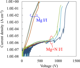
Fig. 6. (Color online) Reverse I–V characteristics of the fabricated GaN pn-diode.
Download figure:
Standard image High-resolution imageFigure 7 plots the breakdown voltage as a function of the net donor concentration. The breakdown voltage improves by the N sequential implantation at any donor concentration. Several studies have found that the N sequential implantation effectively reduces the N vacancies.30,31) Using CV measurements, PL, and positron annihilation spectroscopy, we reported that N sequential implantation reduces hole traps due to N vacancies.22) Therefore, the breakdown voltage improves due to the enhanced pn junction characteristics. Unfortunately, the forward characteristics of the fabricated pn-diodes and/or electrical properties of the Mg implanted layer itself have not yet to be evaluated since the p-type contact is not sufficiently improved and ohmic contact is not obtained. Consequently, evaluating the activation ratio of the Mg implanted layer is a future task.

Fig. 7. (Color online) Donor concentration dependence of the breakdown voltage of the fabricated GaN pn-diode.
Download figure:
Standard image High-resolution image3.2. Results of the vertical GaN planar MOSFET
Figure 8 shows the Id–Vd output characteristics on fabricated GaN MOSFETs. The fabricated MOSFETs show normal MOS channel behaviors such as a suitable drain current control by the gate voltage, good ohmic contact, and a low gate leakage current (<1.0 × 10⁻³ A cm−2). The on-resistance determined from the slope of the Id–Vd curve at Vg = 30 V and Vd = 1 V is 2.78 mΩ cm2.
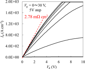
Fig. 8. (Color online) Id–Vd output characteristics of the fabricated vertical GaN planar MOSFET.
Download figure:
Standard image High-resolution imageFigure 9 shows the Id–Vg transfer characteristics of the simultaneously formed lateral GaN MOSFETs on the Mg implanted region. The effects of the parasitic resistance must be eliminated to evaluate the MOS channel property. Hence, the long channel MOSFETs with a 100 μm channel length (Lch) and a 100 μm gate width (Wg) were fabricated. The Vth was determined as the gate bias intercept from the linear extrapolation of Id based on the current equation of linear region,32)

which corresponds to the strong inversion point. Here, μfe is the field effect mobility and Cox is the gate oxide capacitance. The Vth is 2.5 V, and the peak of μfe is 159 cm2 V−1 s−1. Vth extracted from the transfer characteristics of the vertical MOSFET is also 2.5 V, suggesting that the device geometry does not significantly degrade the channel.
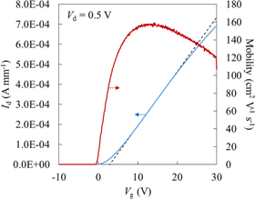
Fig. 9. (Color online) Linear region Id–Vg transfer characteristics of simultaneously formed lateral MOSFETs measured at Vd = 0.5 V. Linear extrapolation for the Vth determination is made at the maximum μfe region.
Download figure:
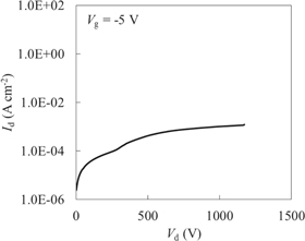
Standard image High-resolution imageFigure 10 shows the breakdown measurement of the fabricated GaN vertical MOSFET. The breakdown voltage was measured while applying −5 V to the gate electrode. The fabricated GaN vertical MOSFET breaks down around 1200 V. The drain leakage current at 1000 V is less than 1.0 × 10⁻³ A cm−2. Therefore, the all ion implantation process can realize a vertical GaN planar MOSFET with a high breakdown voltage of 1200 V and a low on-resistance of 2.78 mΩ cm2.
Fig. 10. (Color online) Id–Vd breakdown measurement of the fabricated vertical GaN planar MOSFET.
Download figure:
Standard image High-resolution image
3.3. Resistance analysis of the vertical GaN planar MOSFET
We evaluated each on-resistance component in the vertical MOSFET using the simultaneously formed test structures to obtain an information for further reduction of the on-resistance. The main resistance components of the fabricated vertical GaN planar MOSFET are attributed to the drift layer resistance, JFET resistance, channel resistance, and source parasitic resistance. The calculated on-resistance of the substrate is 0.27 mΩ cm2 from the specific resistance of 6.7 mΩ cm and thickness of about 400 μm. However, the substrate resistance should be reduced to 1/10 or less because the substrate is sufficiently thick relative to the active region and the current spreads in the substrate. Therefore, the substrate resistance is negligible.
Firstly, we evaluated the resistance of the test structure where Si was implanted into all surface regions of the vertical MOSFET. The calculated resistance of this structure, which consists of the JFET resistance and the drift layer resistance due to the negligible MOS-region and source access resistances, is 1.02 mΩ cm2. According to the previous report,2) the maximum electron mobility in a high-quality n-GaN drift layer grown on a GaN free-standing substrate is 930 cm2 V−1 s−1 at a Si concentration of 8 × 1015 cm−3. Considering the current spread from the narrow JFET area with a width of 1 μm to the drift layer, the estimated resistance of JFET and the drift layer with an electron mobility of 930 cm2 V−1 s−1, carrier density of drift layer of 1 × 1016 cm−3, thickness of 10 μm, and carrier density of JFET region of 1 × 1017 cm−3 is 1.05 mΩ cm2. This calculated value agrees well with the measured one. In addition, the resistance of this test structure without O ion implantation is 3.01 mΩ cm2, confirming that O ion implantation significantly reduces the JFET resistance.
Secondly, the channel resistance was calculated from the resistance of vertical MOSFETs with different channel lengths, a large JFET length and a large cell pitch of 8 μm. In such devices, the difference in the resistance corresponds to the difference in the channel resistance because the drift layer resistance and source parasitic resistance are the same while the JFET resistance is negligible due to the large JFET length of 3 μm. By converting the channel resistance obtained from these devices with a cell pitch of 8 μm into a cell pitch of 5 μm, the channel resistance is 0.38 mΩ cm2. On the other hand, the sheet channel resistance of simultaneously formed lateral GaN MOSFETs is about 7700 Ω sq−1. Furthermore, in the active region of the vertical GaN planar MOSFET, 38 MOS channel regions with a 40 μm width and 1 μm length are connected in parallel. Therefore, the channel resistance assumed from the sheet resistance is 0.26 mΩ cm2. The slight difference between the two calculation methods is attributed to the difference between the designed and actual channel length.
The remaining resistance of 1.38 mΩ cm2 is the source parasitic resistance caused by the source electrode being in contact with the active region in the horizontal direction. This value agrees well with the expected source parasitic resistance of 1.4 mΩ cm2 calculated from the source sheet resistance. This parasitic resistance can be reduced by applying a stacked electrode in vertical contact with the source implanted region.
Therefore, the effective on-resistance of the active region excluding the source parasitic resistance is 1.4 mΩ cm2.
4. Conclusion
In summary, a vertical GaN planar MOSFET is fabricated by an all ion implantation process. The fabricated MOSFET shows an on-resistance of 2.78 mΩ cm2 and a breakdown voltage of 1200 V by applying the short cell pitch design to reduce the on-resistance and the Mg and N sequential implantation to improve the breakdown voltage of the pn-junction. By evaluating each on-resistance component in the fabricated vertical GaN planar MOSFET using the simultaneously formed test structures, an effective on-resistance of the active region excluding the source parasitic resistance is 1.4 mΩ cm2, demonstrating that the all ion implantation process can realize a vertical GaN planar MOSFET with a high breakdown voltage and low on-resistance. This result will greatly contribute to the realization of GaN power devices.
Acknowledgments
This work was partly supported by the Council for Science, Technology and Innovation (CSTI), Cross-ministerial Strategic Innovation Promotion Program (SIP), "Next-generation power electronics" (funding agency: NEDO). Part of this work was conducted at the AIST Nano-Processing Facility, which was supported by the "Nanotechnology Platform Program" of the Ministry of Education, Culture, Sports, Science and Technology (MEXT), Japan. The authors would like to thank K. Nakagawa of the Univ. of Yamanashi for the assistance with SiO2 deposition by a plasma-CVD apparatus.