

Abstract
An all-optical modulator with high modulation efficiency based on a graphene-plasmonic slot waveguide structure is proposed. The modulation efficiency is enhanced by the strong interaction between the light and the graphene–plasmonic structure. A modulation efficiency of 0.21 dB μm−1 is obtained with the signal light at a wavelength of 1550 nm. A graphene–plasmonic slot waveguide device of length of 10 μm is fabricated in the experiment. Benefiting from the strong modulation, it is a promising candidate as an on-chip optical modulator with high modulation efficiency and micrometer-scale footprint.
Export citation and abstract BibTeX RIS
The optical modulator, as a key element in optical communication, is an important requirement for achieving future optical interconnects. The modulator footprint should be at the micrometer scale and the modulation depth needs to be larger than 7 dB, which requires high modulation efficiency.1,2) Current optical modulators, such as those based on LiNO33) and Si,4) are always at centimeter or millimeter scales, and suffer from large device size and low modulation efficiency.
Graphene has provided a way to achieve high performance and fabricate integration modulators owing to its excellent nonlinear optical properties5,6) and CMOS compatibility.7,8) Graphene-based modulators, including electro-optical9–13) and all-optical,14–19) have been reported in recent years. Reference 9 reported a graphene-based Si waveguide modulator with a modulation efficiency of 0.1 dB μm−1. Subsequently, a graphene-based all-optical modulator with micro-fiber was exhibited with a modulation depth of 38% (graphene-cladded length 16 μm).16) However, both types of modulator suffer from low efficiency because of the weak interaction between graphene and the propagating light.
Plasmonic waveguides20–25) are expected to achieve high modulation efficiency since they can provide smaller volumes of propagating modes and local field enhancement. Reference 20 presented an electro-optical modulator combining a graphene and plasmonic waveguide. The modulation efficiency was only about 0.03 dB μm−1, which did not reach achieve the desired results. Recently, an electro-optical modulator based on a Si-plasmonic hybrid waveguide was demonstrated where the excited surface plasmon polariton (SPP) leaky mode in the plasmonic slot waveguide could interact with the graphene sufficiently, achieving a modulation efficiency of 0.13 dB μm−1.22) However, a dielectric layer (Al2O3) was present between the graphene and plasmonic slot waveguide, directly limiting the interaction between the graphene and the leaky mode. This limitation can be overcome in all-optical modulators without a dielectric layer, and the modulation efficiency can be further improved.
In this work, an all-optical modulator based on a graphene–plasmonic slot waveguide (GPSW) is built to enhance the light–graphene interaction via the SPP mode. In this waveguide structure, SPPs are highly confined in the slot waveguide and cause the light–graphene interaction to be enhanced significantly. With this mechanism, a modulation efficiency of 0.21 dB μm−1 is obtained in the fabricated optical modulator with a footprint of 10 μm.
Figure 1(a) depicts the configuration of the all-optical modulator based on the GPSW. The device consists of three sections. In section 1, the signal light is coupled into the Si waveguide and converted into propagation mode by a grating coupler. In section 2, the propagation mode is converted into the SPPs by a taper tip and confined in the plasmonic slot waveguide. A monolayer graphene strip adheres tightly to the waveguide and interacts with the propagated SPP wave in the slot waveguide. In section 3, the signal light is coupled out for detection using another grating coupler. When introducing the modulation light, due to the Pauli blocking effect26–30) the absorption of the signal light changes. Thus, the output of the signal light can be tuned by varying the modulation light power.
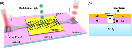
Fig. 1. (Color online) (a) Schematic illustration of the GPSW all-optical modulator. (b) Cross section of the GPSW device.
Download figure:
Standard image High-resolution imageThe cross section of the GPSW structure is shown in Fig. 1(b). The plasmonic slot waveguide consists of a Au slot and Si slot supported by a SiO2 substrate. H and W represent the etched depth of the bottom Si slot and the width of both the Si and Au slots respectively. The upper Au slot will introduce a strong graphene–light interaction by exciting the SPPs. The bottom Si slot with high refractive index will further enhance the SPP confinement in the waveguide and reduce the propagation loss at the Au interface by attracting the propagation mode into the Si slot.
The parameters of the GPSW structure are now analyzed. Finite-element analysis is used to simulate the GPSW structure and the TE mode is selected to ensure that the SPPs are excited in the slot. Since the performance of the modulator will be enhanced for the interaction between the high confinement SPPs and the graphene, it is evaluated as the modulation efficiency. The Fermi level of graphene is tuned from 0.22 eV to 0.41 eV (based on the calculation of the graphene Fermi level) in the simulation of the GPSW structure.
The modulation efficiency dependence on the etched depth of Si slot is presented in Fig. 2(a). The results indicate that the modulation efficiency increases along with the etched depth, and the trends for different slot widths are consistent. This reveals that the larger etched depth of Si can contribute to a stronger graphene–SPP interaction for the GPSW. Thus we fix the etched Si slot depth as 140 nm in the subsequent analysis. As shown in Fig. 2(b), the modulation efficiency (blue line) decreases as the slot width increases. This means that a wider slot can weaken the graphene–SPP interaction. In addition, the field distribution in Fig. 2(c) shows the SPP confinement at different slot widths. It is found that a narrower slot can provide a larger modulation efficiency since it excites higher optical field confinement and a stronger graphene–SPP interaction. According to the propagation loss of the plasmonic slot waveguide [pink curve in Fig. 2(b)], a narrower slot suffers a larger propagation loss. Thus, a trade-off between the propagation loss and the SPP confinement should be considered. Based on this analysis, a slot width of 80 nm and depth of 140 nm are selected in the following fabrication and experiment. The theoretical modulation efficiency is 0.35 dB μm−1 under the optimized parameters.

Fig. 2. (Color online) Simulated results for the GPSW. (a) Modulation efficiency as a function of etched Si height. (b) Modulation efficiency and the propagation loss at different slot widths. (c) Field distribution showing the SPP confinement at slot widths of 20 nm, 80 nm, and 160 nm. All three mode distributions share the same color bar.
Download figure:
Standard image High-resolution imageThe fabrication process of the GPSW device is shown in Fig. 3(a). First, the Si device including grating couplers, waveguide, and tapers was fabricated on a commercial silicon-on-insulator wafer (220 nm Si layer and 2 μm buried oxide layer), and its height was 80 nm. Then, the area between the two tapers was exposed. A Au sheet with a thickness of 80 nm was deposited onto the wafer by magnetron sputtering. Subsequently, the plasmonic slot was etched using the focused ion beam technique. The Au and Si slots were etched to 80 nm and 140 nm depth, and both were fabricated 80 nm wide and 10 μm long. Finally, the graphene was transferred onto the plasmonic slot waveguide and the unwanted region was removed by oxygen plasma etching.
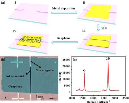
Fig. 3. (Color online) Fabrication and characteristic of the GPSW device. (a) Schematic illustration of the fabrication process for the GPSW. (b) False-color scanning electron microscopy image of the GPSW device. (c) Raman spectrum of a monolayer graphene sheet.
Download figure:
Standard image High-resolution imageThe fabricated GPSW device is exhibited in Fig. 3(b), and the transferred graphene on the plasmonic slot waveguide is clearly seen in the green areas. Raman spectroscopy is performed to characterize the graphene in Fig. 3(c). The Raman intensity ratio of the G peak and the 2D peak is 0.617, which demonstrates that the graphene is approximately monolayer.15,19)
Next, the modulation performance of the GPSW device was measured using the optical system shown in Fig. 4(a). A laser wavelength of 532 nm with spot diameter 160 μm provided the modulation light. Different modulation powers can be achieved by exploiting a tunable attenuator. The signal light was from a CW-semiconductor laser (TFL-C-20) with the power fixed at 1 mW. The signal light was coupled in and out from the modulator by fiber alignment to the grating coupler on the fabricated device. The output light was detected by an Optical Spectrum Analyzer (AQ6370D, detection wavelength: 600–1700 nm). The output power of the signal light at the wavelength of 1550 nm is represented in Fig. 4(b) under the different powers of the modulation light. When the value of the modulation power is zero, the output power of the signal light is low due to the light being absorbed by the graphene. The red spheres represent the experimental data showing the output power in dBm increasing with the modulation power. The black line is the linear fitted curve, which is basically in agreement with the experiments. The modulation depth is defined as the difference in the output power of the signal light. The maximum modulation depth is 2.1 dB in the experiment. The modulation efficiency is achieved by normalizing the modulation depth to unit length. The result shown in Fig. 4(c) indicates that the modulation efficiency in dB keeps increasing and remains linear with the modulation light power. The maximum modulation efficiency is 0.21 dB μm−1. This value is a little lower than the theoretical estimate of 0.35 dB μm−1, since some partial damage to the transferred graphene influences its absorption.15)
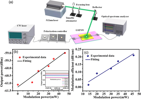
Fig. 4. (Color online) Performance of the GPSW all-optical modulator. (a) Measurement system for the GPSW device. (b) Dependence of the output spectra of the GSPW device on the modulation light power at 1550 nm. The inset is the signal light wavelength dependence of the modulation power. (c) Changes in the modulation efficiency for the signal light at 1550 nm.
Download figure:
Standard image High-resolution imageFinally, the mechanism of the all-optical modulator based on the Pauli blocking effect is analyzed. In Fig. 5(a), when introducing the modulation light with high intensity, the carrier concentration increases, which leads the states near the edge of the conduction and valence bands to be filled. Since one state cannot contain two electrons, Pauli blocking takes place. This shifts the absorption threshold into a higher frequency, resulting in a much lower absorption of signal light. Thus, increasing the modulation light power can limit the absorption of signal light, which means that the output of the signal light can be tuned by the modulation light in the GPWS device. Specifically, signal light absorption decreases with modulation power, contributing to an output increase of the signal light. Thus the total concentration can be written as


Fig. 5. (Color online) (a) Graphene Pauli blocking effect. (b) Absorption coefficients of the signal light.
Download figure:
Standard image High-resolution image
For absorption much less than the saturable absorption, the carrier concentration will be related to the average optical intensity by28,31)  where the α, I, τ, and ω are absorption coefficient, average optical intensity, electron–hole recombination time, and optical frequency, respectively.
For zero band gap graphene,29) the electron–hole recombination time τs is ∼1 ps for the signal light, Is = 3.3 × 10⁴ W cm−2 (2.1 × 10⁻⁶ mW/80 × 80 × 10−14 cm2), and ωs is the signal light frequency (1550 nm). Graphene can absorb 2.3% of incident visible and near-infrared (2.3% absorption for both signal light and modulation light). Thus the carrier concentration ( ) can be obtained. Im is average optical intensity, 2.3 × 10² W cm−2 (46 mW/π*802 μm2, 46 mW is the maximum modulation power in the experiment), τm ∼ 106 is the carrier recombination time for modulation light,30) ωm is the modulation optical frequency of 532 nm. Thus the carrier concentration of the modulation light can be calculated. The graphene Fermi level depends on carrier concentration, according to the equation:
  and thus the Fermi level of graphene can be calculated. When only the signal light is present, the Fermi level is 0.22 eV. With the addition of the modulation light, the modulated Fermi level is 0.41 eV.
For the signal light, the absorption coefficient is expressed as

Both the output power of the signal light Ps (Ps =  ) and the modulation efficiency (ME) in dB depend on the absorption coefficient αs:


where 
According to Eqs. (3) and (4), the output power of the signal light and the modulation efficiency both change linearly with the intensity of the modulation light. This accords with the experiment results in Figs. 4(b) and 4(c). Obviously, the graphene absorption is much less than the saturable absorption. Hence, the modulation efficiency could be further enhanced by increasing the modulation light power.
The signal light absorption coefficient of the GPSW device is presented based on Eq. (3) and the result is shown in Fig. 5(b). The decrease in absorption coefficient agrees well with the Pauli blocking effect, indicating that the experiment results are consistent with theory. In the experiment, a 50% change in the absorption coefficient is obtained in the GPSW device. This is due to the strong interaction between the graphene and the SPPs in the GPSW structure.
In summary, an all-optical modulator based on the GPSW structure has been presented. The structure parameters are analyzed by simulation to guarantee a sufficient light–graphene interaction. Experimentally, a modulation efficiency of 0.21 dB μm−1 and a compact footprint are achieved. This result indicates that the GPSW-based modulator can provide an improved method of achieving high-efficiency modulation for future on-chip interconnection.
Acknowledgments
This work was supported by the National Science Foundation of China (61705229, 61775213, 61475199, 31501084), the CAS Western Light Program 2015, Natural Science Foundation of Chongqing (Cstc2016jcyjA0314), Technology Innovation and Application Demonstration Research Project of Chongqing (cstc2018jscx-msybX0084) and State key research and development funding (2017YFB1002900).