

Abstract
We propose a high-quality multispectral plasmonic sensor by coating a dielectric grating on the semiconductor-metal-semiconductor stacks. Ultra-narrow plasmonic resonances with the minimum bandwidth of 8 nm are insensitive to the polarization of incident light. The ultra-narrow multi-band phenomenon can be ascribed to the synergy of guided mode resonances, cavity modes and surface plasmon polaritons. The sensor displays superior refractive index sensitivity (404.295 nm/RIU) and figure of merit (50.3) and can also be used to detect the protein layer in sub-nanometer thickness. These offer new perspectives for achieving ultra-compact efficient sensors and filters.
Export citation and abstract BibTeX RIS
With the rapid development of nanophotonics, metal nanostructures have attracted significant interest of the research community in many application fields due to the excitation of surface plasmon polaritons (SPPs).1–3) SPPs are essentially electromagnetic waves which travel along the metal/dielectric interface and can be tailored by tuning the structural parameters, which enables the structure to own the unique capability in control of light.4–7)
Since the extraordinary optical transmission was demonstrated by Ebbesen et al. in 1998,1) much attention has been drawn to the research of metal transparency due to its potential application in transparency electrodes,8) sensing9) and cloaking.10) To make the metal film transparent, a typical approach is to introduce holes or slits in both sides of the metal film, which could provide the efficient coupling of input and output light by exciting the surface plasmons.11) Interestingly, narrow dips in the high transmission spectrum were also found to have wide applications in sensor field.9,12,13) For example, Chen et al. proposed a U-shaped split-ring array structure to achieve transmission dips for sensing.9) Lin et al. proposed a InSb film with a metal surface grating to serve as a sensitive SPP sensor.12) However, the transmission dips in these structures are shallow and only work in the near-infrared and THz ranges. Semiconductor–metal–semiconductor (SMS) stacks have also been proved with broadband optical transparency.14) However, the optical sensing based on this kind of structure has not been studied in depth.
In this work, we theoretically proposed an ultra-narrow multispectral sensing platform through coating a dielectric grating on the SMS stacks (GSMS). Three obvious transmission dips are observed in the visible and near-infrared regions with the minimum full-width at half-maximum (FWHM) of 8 nm. A high-quality sensor is thus achieved with the sensitivity S approaching to 404.295 nm/RIU (RIU means the refractive index unit) and figure of merit (FOM) exceeding 50.5. In addition, the proposed structure is tunable by changing the structural parameters. Therefore, this GSMS structure can be applied in the high-quality sensing, light flow manipulating and filters.
The proposed GSMS structure consists of a one-dimensional Al2O3 grating array standing on a three-layer SMS structure as depicted in Fig. 1(a). The period, width and thickness of grating are denoted as P, W, and H, respectively. The thicknesses of the bottom and top Si films and Au film are depicted by h1, h2 and h, respectively. The optical performance of the GSMS structure was calculated by the three-dimensional finite-difference time-domain method.15) The dielectric constant of Si is taken from the experimental data by Palik.16) The dielectric permittivity of Au is described by Drude model.17) The refractive index of Al2O3 is n = 1.75. Since the structure can be treated infinitely along y direction, a simplified two-dimensional simulation model is applied. Periodic boundary conditions are used in x direction while perfectly matched layers are applied in z direction. The plane wave with a wide frequency range is used as the light source. This structure can be prepared by magnetron sputtering and electron beam lithography.18–20) Firstly, the SMS stacks can be fabricated by sputtering the related materials on the silica substrates in turn. Then, a layer of photoresist would be coated on the SMS stacks and etched by the electron beam lithography to form one-dimensional period strips. After that, the Al2O3 grating would be sputtered on the photoresist strips and then the lift-off method would be used to remove the photoresist strips coated with the Al2O3 layers to obtain the GSMS structures.

Fig. 1. (Color online) (a) Schematics of the GSMS structure. (b) Transmission spectra of GSMS, SMS and Al2O3 grating. Electric field ∣E∣ and magnetic field ∣H∣ distributions of dips λ1 (c), (d), λ2 (e), (f), and λ3 (g), (h), respectively. Here, P = 600 nm, W = 300 nm, H = 200 nm, h1 = h2 = 30 nm and h = 20 nm.
Download figure:
Standard image High-resolution imageFigure 1(b) shows the transmission spectra of the proposed GSMS structure (black solid line), Al2O3 grating (green dash dot line) and three-layer SMS film stacks (purple dash line) with the same structural parameters. For the SMS stacks, only a broadband transparent window is observed. For the Al2O3 grating, two dips are achieved, one is steep and the other is very shallow. Interestingly, by placing the Al2O3 grating on the SMS stacks (i.e., GSMS structure), two ultra-narrow dips and one broad dip are obtained at 641 nm (λ1), 825 nm (λ2) and 1220 nm (λ3) with the minimum FWHM of 8 nm. For the dip λ1, the electric field (∣E∣) mainly distributes at the four corners of the grating strips [Fig. 1(c)] and strong magnetic field (∣H∣) is located in the grating strips [Fig. 1(d)]. These indicate the excited guide mode resonances (GMRs) of Al2O3 grating,20,21) which contribute to the coupling of light into the structure and further excite the SPPs of metal film. Moreover, the energy located in the top Si film implies the excited cavity mode.22) For the dip λ2, besides the corners of grating strips and the interfaces of Si/air, there also exist strong electric field in the bottom Si film and strong magnetic field in the SMS stacks [Figs. 1(e) and 1(f)]. These indicate that the GMRs, cavity modes and SPPs dominate this resonant dip. For the dip λ3, only weak electric field is found in the grating slots and the two Si films and the magnetic field is mainly concentrated in the SMS stacks [Figs. 1(g) and 1(h)]. It can be concluded that this dip is closely related to the cavity modes and SPPs.20–22)
To further insight into the phenomenon, we investigate the influence of grating width W on the resonances as shown in Fig. 2(a). Pronounced red-shifts are observed with the increased W. It is because that the increased W will lead to the increase of effective refractive index,21) which can be explained qualitatively by the waveguide mode theory.23) Figure 2(b) depicts the dependence of dips on the period P. It can be clearly seen that the three dips all have red-shifts as P increases. These can be ascribed to the transverse wavevector of waveguide modes in the dielectric layers. The wavevector is given by  where θ is the incident angle.21,23) Specific resonant wavelength can couple the incident light into the waveguide modes when the grating period P is different. Therefore, the red-shifts of resonant dips with the increased P can be interpreted by the plasmon dispersion theory.24)

Fig. 2. (Color online) Transmission spectrum of the GSMS with (a) different W and fixed P = 600 nm and (b) different P and fixed W = 300 nm. Other parameters H = 200 nm, h1 = h2 = 40 nm and h = 20 nm.
Download figure:
Standard image High-resolution imageIn Fig. 3(a), continuous red-shifts are observed for these three dips when the thicknesses of both Si films simultaneously increase from 0 to 40 nm (h1 = h2). These are mainly because that the effective cavity length of dielectric layers increases.25) In Fig. 3(b), when the thickness of Al2O3 grating (H) increases from 100 to 220 nm, the dip λ2 slightly moves to the longer wavelength range, demonstrating that the dominant role of GMRs on this resonance.26) While for the dips λ1 and λ3, the depths of both dips increase with H, accompanied by obvious red-shifts, which imply the important role of cavity modes on these two resonances due to the effective cavity length.26) Figure 3(c) shows the transmission responses for the structure with a tunable h. With increasing h from 15 to 30 nm, the dips λ1 and λ2 both display obvious red-shifts but the dip λ3 shows a pronounced blue-shift. The red-shifts of dips λ1 and λ2 can be explained by the wavevector matching conditions21) due the increase of the effective refractive indices of the GMRs. The wavelengths of GMRs inevitably are raised to match the wavevectors of SPPs.21) The blue-shift of λ3 mainly results from the deteriorated charge distribution on the metal's surface due to the finite skin depth.27)

Fig. 3. (Color online) Transmission spectra of the GSMS structure with different (a) h1 (here h1 = h2, h = 20 nm and H = 200 nm), (b) H (h = 20 nm and h1 = h2 = 40 nm) and (c) h (h1 = h2 = 40 nm and H = 200 nm). Other parameters P = 600 nm and W = 300 nm.
Download figure:
Standard image High-resolution imageWe also calculated the transmission evolution for the GSMS structure with asymmetric thickness difference (Δh = h2 − h1) of the two Si films. When Δh increases from −20 to 0 nm by keeping h1 = 40 nm and increasing h2 from 20 to 40 nm, three dips all display obvious red-shifts, accompanied by the deepening depth as shown in the bottom figure in Fig. 4(a). When Δh increases from 0 to 20 nm by keeping h2 = 40 nm and decreasing h1 from 40 to 20 nm, pronounced blue-shifts are achieved, accompanied by the shallowing depth in the top figure in Fig. 4(a). The frequency-shifts mainly originate from the reduced effective refractive of the top or bottom Si films. The shallowing dips result from the asymmetric coupling between the top and bottom Si films. The optimal optical property is obtained as Δh = 0. The effect of polarization angle on the structure performance was also calculated as shown in Fig. 4(b). Obviously, the dips λ1 and λ2 are independent on the polarization angle. The dip λ3 almost disappears when the polarization angle is larger than 50° due to that this resonance is dominated by SPPs.
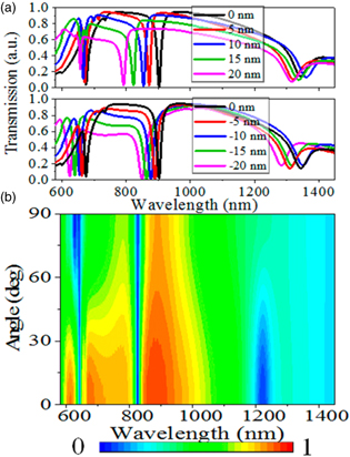
Fig. 4. (Color online) Transmission spectra for the GSMS structure with asymmetric thickness difference (Δh = h2 − h1) of two Si films. Top: h2 = 40 nm, h1 changes. Bottom: h1 = 40 nm, h2 changes (P = 600 nm, W = 300 nm, H = 200 nm and h = 20 nm). (b) Polarization angle resolved spectrum response of GSMS structure. Parameters in (b) are the same as those in Fig. 1(b).
Download figure:
Standard image High-resolution imageWe further explored the potential of the GSMS structure for sensing applications. In Fig. 5(a), noticeable spectral shifts of three dips are observed when the environment index is varied from 1.000 to 1.040 in intervals of 0.005. The linearly fitted sensitivity S (S = Δλ/Δn, Δλ and Δn are the wavelength shift and refractive index change, respectively)28–30) for dips λ1, λ2 and λ3 are 404.295, 320.045 and 181.9 nm/RIU, respectively. The FOM (FOM = S/FWHM) is more meaningful to evaluate the sensor quality28–30) and strongly depends on the resonant bandwidth. For the dip λ2, the FOM is 50.53, indicating the high-performance sensing. An alternative dimensionless FOM* = ∣(ΔI(λ)/Δn(λ))/I0(λ)∣max is also considered at a fixed wavelength (λ) with the relative intensity (I) change ΔI induced by Δn.28) The maximum FOM* approaches to 335.14 at 825 nm. Correspondingly, the optoelectronic detection signal changes from the "dark" state (T = 0.0462) to the "bright" state (T = 0.6655). That is, the remarkable intensity change behavior from near opaque to transparency is achieved through the spectral shifts after a slight change of surrounding refractive index. These findings indicate the efficient sensing feature of the GSMS structure.

Fig. 5. (Color online) (a) Spectral shifts of dips (λ1, λ2, and λ3) with the surrounding refractive index changing from 1.000 to 1.040 with a step of 0.005. (b) Spectral shifts of dips λ1 and λ2 with the protein layer thickness increasing from 0 to 30 nm in an interval of 5 nm. Inset: schematic of adsorbed protein layer on the structure. Parameters P, W, H, h1 (=h2) and h are 600, 300, 200, 30 and 20 nm, respectively.
Download figure:
Standard image High-resolution image
The bio-sensing performance was further carried out by localizing the protein molecules on top surface of the grating in the GSMS structure as the inset shown in Fig. 5(b). The molecular film is expected to have a refractive index of 1.45 in the visible and near-infrared regions.31) Based on the strong electromagnetic enhancement effects, obvious red-shifts of dips λ1 and λ2 are obtained as the thickness of the protein layer increases from 0 to 30 nm. This further verifies of the sensing advantages of the GSMS structure.
We have theoretically proposed a simple and powerful ultra-narrow multispectral sensor with polarization insensitivity based on the SMS film stacks coated by a dielectric grating. The multispectral plasmonic sensor displays superior S (404.295 nm/RIU), FOM (50.3), and FOM* (335.14) with the minimum FWHM of 8 nm. In addition, the sensor platform can also be used for the detection of bio-molecule layer with sub-nanometer thickness coating on the grating. These hold the proposed scheme with potential applications in the high-quality sensors, high power light manipulating and filters.
Acknowledgments
We gratefully acknowledge support from National Natural Science Foundation of China (51761015, 11564017, 11804134, 11464019, and 11764022), and Natural Science Foundation of Jiangxi province (20181BAB201015, 20182BCB22002 and 2018ACB21005).