
Abstract
The three-dimensional imaging of threading dislocations in GaN films was demonstrated using two-photon excitation photoluminescence. The threading dislocations were shown as dark lines. The spatial resolutions near the surface were about 0.32 and 3.2 µm for the in-plane and depth directions, respectively. The threading dislocations with a density less than 108 cm−2 were resolved, although the aberration induced by the refractive index mismatch was observed. The decrease in threading dislocation density was clearly observed by increasing the GaN film thickness. This can be considered a novel method for characterizing threading dislocations in GaN films without any destructive preparations.
Export citation and abstract BibTeX RIS

Content from this work may be used under the terms of the Creative Commons Attribution 4.0 license. Any further distribution of this work must maintain attribution to the author(s) and the title of the work, journal citation and DOI.
GaN-based semiconductors have attracted much attention for a wide range of applications in optical devices, such as ultraviolet- and visible-light-emitting devices,1,2) and electronic devices, such as high-frequency and high-power transistors.3) In device fabrications, the lack of a native GaN substrate imposes epitaxial growth on substrates consisting of foreign materials.4–7) The large lattice mismatch and the difference in thermal expansion coefficient between a foreign substrate and an epitaxial layer result in threading dislocations with a density as high as 106 to 1010 cm−2. This density depends on the substrate, film thickness, and epitaxial growth method used. These dislocations degrade the device performance. For GaN-based devices, GaN substrates with a low defect density are basically required.8,9) In order to fabricate bulk GaN crystals with a low threading dislocation density, there have been many attempts of using growth methods, such as halide vapor phase epitaxy (HVPE),10) etc.11–13) HVPE is currently recognized as the preferred method for fabricating bulk GaN substrates with relatively high purity and low cost because it has the highest growth rate among the other growth methods. With respect to the threading dislocation density, both the ammonothermal and Na flux methods have been superior.14,15) Thus, there are still discussions on how to fabricate a bulk GaN crystal with large diameter, low dislocation density, and low cost.
The threading dislocations in the GaN crystal can propagate along the epitaxial direction. On the other hand, it is well known that these dislocations annihilate in pairs and their density decreases with increasing epitaxial layer thickness.16) In developing a growth method that can promote this annihilation, the propagation property of threading dislocations should be precisely observed. For such observation, several methods, such as transmission electron microscopy (TEM),17) the etch pit method,18) and cathode luminescence (CL) measurement,19) can be used. TEM can precisely identify the type of dislocation through electron diffraction; however, a complicated and delicate sample preparation process is necessary. Nevertheless, the observation area is limited to a few µm2. The etch pit method can only exhibit the dislocations at the surface and it is difficult to use it to track the motion of dislocations. In addition, these two methods are destructive. CL measurement is useful for characterizing the distribution of dislocations near the surface of an epitaxial film because this is a nondestructive analysis method. The CL intensity becomes low around the dislocations that act as nonradiative centers. As a result, dark spots can be observed around the dislocations in the CL image. Unfortunately, CL can show only the distribution of dislocations near the surface because the penetration depth of irradiated electrons is about 1 µm. In the applications for vertical devices, it is desired that the defect properties inside epitaxial layers be investigated using a nondestructive method.
In this study, a novel method for characterizing threading dislocations using a two-photon excitation microscope is described. This method has been developed as a bioscience imaging technology for visualizing in vivo living tissues.20–22) In this method, the excitation wavelength is longer than the photoluminescence (PL) wavelength. The two-photon absorption process is different from the conventional absorption process, in which the excitation wavelength is shorter than the PL wavelength. The excitation probability in the two-photon absorption nonlinearly depends on the excitation photon intensity. When the excitation light is focused into the inside of the sample, photocarriers are generated at the focal point. Then, PL occurs near the focal point through some carrier diffusion processes. In semiconductor materials, this nonlinear process has been studied.23) Two absorption properties were studied in GaN,24) and subsequent PL properties were observed.25) By combining the two-photon absorption process, the nonradiative properties of dislocations, and the sweep of the focal point, the three-dimensional image of dislocations can be constructed. In the previous studies of SiC, defect characterization by, for example, crystallographic phase analysis and dislocation imaging, was performed.26–28) The obtained results indicate that this method can be considered useful for characterizing the defects in GaN. Moreover, this method is more suitable for GaN than for SiC. The reason for this is that GaN shows a much stronger PL than SiC because GaN is an optically direct transition material different from SiC. However, GaN has an absorption coefficient of 105 cm−1, which is one order of magnitude larger than that of SiC. This large absorption coefficient sometimes disturbs the extraction of PL emitted from the inside of a crystal. In this study, a method of observing two-photon excitation photoluminescence (2PPL) over all the GaN samples is investigated to determine the behavior of dislocations in thick GaN films. The three-dimensional imaging of threading dislocations in GaN films is demonstrated.
The five samples prepared were a free-standing c-plane bulk GaN substrate, a free-standing m-plane bulk GaN substrate, a 2-µm-thick c-plane GaN thin film grown on a sapphire substrate by metalorganic vapor phase epitaxy (MOVPE), and two c-plane GaN thick films grown on GaN/sapphire templates by HVPE. Both m- and c-plane bulk GaN substrates were prepared by slicing the c-plane HVPE-grown crystals. The TD densities of these bulk GaN substrates were about 106 cm−2. The thicknesses of the HVPE-grown c-plane GaN films are 160 and 320 µm. A two-photon excitation microscopy system (Nikon A1MP series) was used for 2PPL measurements. The measurements were performed in air atmosphere at room temperature. The excitation source was a Ti-sapphire mode-locked laser with a wavelength of 700 nm. The laser was operated in the pulse mode with a pulse width of 100 fs and a repetition rate of 80 MHz. The average excitation power was adjusted within 1–14 mW. The laser beam was focused using an objective lens with a magnification of 50. The intensity of the near-band-edge (NBE) emission in GaN was measured using a GaAsP photomultiplier tube through an optical bandpass filter with a center wavelength of 370 nm and a bandwidth of 38 nm. An in-plane area of 32 × 32 µm2 was scanned using Galvano scanning mirrors, and 1024 × 1024 pixels were recorded. The focal depth along the Z-direction was changed using a stepping motor with a 0.2 µm step. A three-dimensional 2PPL image was constructed from the in-plane 2PPL images measured at various focal depths. Owing to the high refractive index of GaN (nGaN = 2.36) compared with that of the measurement atmosphere (nair = 1), the actual measurement depth was expanded with a magnification of nGaN/nair.
For observing the 2PPL from the deep area, self-absorption should be considered. The 2PPL spectrum near the NBE emission of GaN was compared with a conventional PL one. In the conventional PL measurement, a He–Cd laser with a peak emission wavelength of 325 nm was used as an excitation source. Figure 1 shows 2PPL and conventional PL spectra from the c-plane bulk GaN substrate. The focal depth of the excitation laser beam in the 2PPL measurement is about 15 µm. It is noted that the different noise levels between the two spectra are due to the dynamic range of the detector. At room temperature, the NBE emission has a peak energy of around 3.42 eV (∼363 nm) as seen in the conventional PL spectrum. This NBE emission has two longitudinal optical (LO) phonon replicas at the lower energy side at 3.34 and 3.25 eV (371 and 382 nm, respectively). The 2PPL spectrum has double peaks at 3.36 and 3.34 eV (369 and 372 nm, respectively) followed by a lower shoulder peak at 3.26 eV (381 nm). The difference between the two spectra is due to the self-absorption phenomenon. To detect the PL emitted from an area deeper than 10 µm, the absorption coefficient should roughly be less than 103 cm−1, which is much lower than about 105 cm−1 at the GaN bandgap energy. Thus, weak optical absorption characteristics in the region called the Urbach spectral tail29) must affect the self-absorption characteristics, which change the lineshape of 2PPL spectra. The 2PPL spectrum in Fig. 1 experimentally showed that the tail of the lower side energy in the NBE emission can be detected even from a deep area in the sample. The LO phonon replicas of the NBE emission have a lower emission energy with a lower absorption coefficient than the NBE emission. Therefore, the LO phonon replicas of the NBE emission can penetrate the inside of the GaN crystal and can be extracted from the outside of the sample. Moreover, two dips appeared at 3.35 and 3.27 eV (370 and 379 nm, respectively) in the 2PPL spectrum as indicated by arrows in Fig. 1. The appearance of these dips indicates the presence of absorption peaks at the LO phonon replicas of the NBE emission and implies the induction of LO-phonon-assisted free-exciton absorption. Such absorption may occur because it is a process almost opposite to that in the LO phonon replicas of the NBE emission. The influence of the absorption process in the 2PPL measurements must be investigated further. In the following experiments, 2PPL in the wavelength range of 351–389 nm is collected using a bandpass filter.

Fig. 1. Comparison of spectral shape between conventional PL (dotted line) and 2PPL (solid line) around the NBE emission of GaN measured from the c-plane bulk GaN substrate.
Download figure:
Standard image High-resolution imageIn order to evaluate the spatial resolution of 2PPL measurements, the images of 2PPL focused on the surfaces of the GaN crystals were observed, and the maximum density of threading dislocations visualized was discussed. Figure 1 shows the in-plane images of 2PPL focused on the surfaces of the samples with various threading dislocation densities. Many dark spots are clearly observed in Figs. 2(a) and 2(b). These dark spots are due to the nonradiative characteristics of threading dislocations as mentioned previously. The dark spot diameter is determined by the effective diffusion length of minority carriers, which are excited carriers.30) Here, the dark spots have a diameter of about 0.6 µm. To independently observe each dislocation, each dislocation should be separated sufficiently. When the threading dislocation density was higher than 1 × 108 cm−2 as shown in Fig. 2(c), each dark spot could not be separately observed in the image because neighboring dark spots could not be spatially resolved. Individual dark spots were visualized when their density was less than 1 × 108 cm−2.
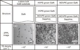
Fig. 2. Surface 2PPL images of GaN crystals with different threading dislocation densities, schematic cross-sectional structures, and threading dislocation densities.
Download figure:
Standard image High-resolution imageBy varying the focal depth, an in-plane 2PPL image at each focal depth can be obtained as shown in Figs. 3(a)–3(c) (see online supplementary data 1 at http://stacks.iop.org/APEX/11/031004/mmedia). By combining all the 2PPL images obtained at various focal planes, a three-dimensional 2PPL image can be constructed (see online supplementary data 2 at http://stacks.iop.org/APEX/11/031004/mmedia). Figure 3(d) shows a three-dimensional 2PPL image of the GaN film HVPE-grown on a GaN/sapphire template. Note that the contrast of this 2PPL image is inverted; thus, dark spots and lines are shown as bright spots and lines, respectively. This HVPE-grown GaN film has threading dislocations with a density of ∼1 × 107 cm−2. All connected dark spots form dark lines, which are thought to correspond to the dislocation features. Some of these lines are observed as dotted lines owing to the large measurement step along the depth direction. Most of the dark lines propagate along the c-axis. This means that dislocations propagate perpendicularly to the growth front with the c-plane.

Fig. 3. In-plane 2PPL images obtained at various focal depths of (a) 0 (at surface), (b) 50, and (c) 100 µm, and (d) three-dimensional 2PPL image of HVPE-grown GaN film. The intensity contrast in the three-dimensional 2PPL image is inverted to visualize dark lines as white lines.
Download figure:
Standard image High-resolution imageFor imaging threading dislocations, the high spatial resolution in the 2PPL measurement is necessary. The spatial resolution is determined by both the diffusion length of minority carriers and the excitation volume. The former is roughly sub-micrometers in n-type GaN. The latter is determined using an optical system. Since the probability of two-photon absorption is proportional to the square of the excitation photon density, the excitation volume is determined by the square of the spread of light in the diffraction phenomenon.31) The excitation volume in the 2PPL measurement system used in this experiment is calculated to be 0.32 and 3.2 µm for both the in-plane and depth directions, respectively. This large value for the depth direction is due to the high refractive index of GaN. In the condensing optical system, the excitation volume along the depth direction is determined by both the numerical aperture and the refractive index. To obtain a small excitation volume along the depth direction, a high numerical aperture is introduced in the system. If the refractive index of the specimen is higher than that of the measurement atmosphere, the focal spot elongates along the depth direction. This is equivalent to lowering the numerical aperture. Another factor that determines the spatial resolution is the aberration of the incident light source. Since a refractive index mismatch exists between air and GaN, a spherical aberration exists. This aberration decreases the spatial resolution, especially for the depth direction.31,32) In this study, the spatial resolution was experimentally investigated from the diameters of dark lines in the three-dimensional 2PPL images. Figures 4(a) and 4(b) show the three-dimensional 2PPL images observed for the m- and c-plane bulk GaN substrates, respectively. These images are contrast-inverted and dark lines are shown as bright ones. The diameters of the dark lines [bright lines in Figs. 4(a) and 4(b)] as a function of the focal depth are shown in Fig. 4(c). The excitation light was irradiated on the surfaces of the samples. For both samples, most of the threading dislocations propagate along the c-axis direction. This result reveals that the threading dislocations are in the in-plane direction for the m-plane bulk GaN substrate as shown in Fig. 4(a), while they are in the depth direction for the c-plane bulk GaN substrate as shown in Fig. 4(b). The diameter of each dark line differs with the direction as expected from the calculated excitation volume. The diameter in the in-plane direction (dxy) is as small as 0.6 µm at a focal depth smaller than 50 µm as shown in Fig. 4(c). dxy is much smaller than the focal depth, so the influence of the surface recombination can be neglected. The constant diameter indicates that the diameter of dark spots is determined by the diffusion length of minority carriers.30) The diameter in the depth direction (dz) is approximately 3 µm larger than dxy near the surface. The contrast of the dark lines is weaker in the m-plane bulk GaN substrate than in the c-plane bulk GaN substrate as shown in Figs. 4(a) and 4(b), respectively. Then, the background noise appears in the three-dimensional 2PPL image in the m-plane GaN bulk substrate as shown in Fig. 4(a). Plots for dz in Fig. 4(c) show a large dispersion owing to several reasons: a weak contrast, a large excitation volume along the depth direction, a large measurement step interval along the depth direction, the existence of dark lines nonparallel to the c-axis, and so forth. Both dxy and dz increase with the focal depth, as shown by dotted lines in Fig. 4(c). This is due to the aberration induced by the refractive index mismatch. This aberration reduces the spatial resolution at a large focal depth. A significant reduction in resolution is observed along the depth direction. In improving the spatial resolution, an oil immersion objective lens, which reduces the refractive index mismatch, can be considered effective.

Fig. 4. Three-dimensional 2PPL images obtained from (a) m-plane and (b) c-plane bulk GaN substrates. (c) Diameters of dark lines along in-plane (dxy) and in-depth (dz) directions as a function of focal depth. The dotted lines serve as visual guides.
Download figure:
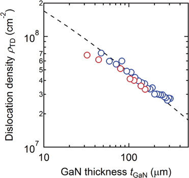
Standard image High-resolution image2PPL measurements enable the investigation of a three-dimensional defect distribution. For example, the dependence of the threading dislocation density on the growth thickness can be analyzed for GaN films HVPE-grown on sapphire substrates. The lattice mismatch between GaN and sapphire generates high-density threading dislocations in the GaN epitaxial film. As the growth thickness increases, the threading dislocation density decreases. To observe the reduction in threading dislocation density with progressing HVPE growth, in-plane 2PPL images are measured at various focal depths. Figure 5 shows the dark spot density as a function of the GaN growth thickness for HVPE-grown GaN films. During the growth, some of the threading dislocations are annihilated by their reaction as theoretically discussed in Ref. 16. As shown in Fig. 5, the theoretical curve plotted with a dotted line is in good agreement with experimental plots.
Fig. 5. Dark spot density as a function of growth thickness for 160-µm-thick (red circles) and 320-µm-thick (blue circles) HVPE-grown GaN films on sapphire substrates. Experimental data were fitted using a dislocation annihilation model.
Download figure:
Standard image High-resolution imageThe three-dimensional 2PPL image also shows the motion of threading dislocations. Figure 6 shows the displacement distribution in 248 dark spots during the 10-µm-thick HVPE growth. This distribution is measured from the three-dimensional 2PPL image of the 320-µm-thick HVPE-grown GaN film in the thickness range from 310 to 320 µm. All the threading dislocations displace within 3 µm in the in-plane direction. We found that the displacement of the threading dislocations along the a-axis is 3 µm, which is larger than those along the other directions. The reason why the threading dislocations can easily move along the a-axis is that the m-plane acts as a prismatic slip plane in a wurtzite structure. Further analyses of threading dislocations will be feasible by 2PPL measurements, such as those for dislocation annihilation/fusion phenomena, dislocation bending at the homoepitaxial growth interface, dislocation multiplication due to strain relaxation, and the interaction of threading dislocations, which will be reported in the near future.

Fig. 6. Movement of the dark spots during the 10-µm-thick HVPE growth, which corresponds to the growth thickness between 310 and 320 µm. NTD indicates the number of measured dark spots.
Download figure:
Standard image High-resolution image
In conclusion, 2PPL measurement enables threading dislocations in GaN crystals to be visualized when their density is less than ∼108 cm−2. This method is very useful because threading dislocations can be characterized without any destructive preparations. We believe that this method will enable us to further characterize III–nitride materials and accelerate the development of GaN-based vertical devices.
Acknowledgments
This work was partly supported by JSPS KAKENHI Grant Numbers JP16K18074 and JP17H05325. The experiments using a two-photon excitation microscope were carried out at the Graduate School of Biomedical Engineering, Tohoku University. We would like to thank Ms. Masako Ino and Mr. Hideo Saisho of Nikon Instech Co., Ltd. for instructing the operation of the two-photon microscope.