

Abstract
We demonstrate true-blue 450 nm tunnel junction (TJ) laser diodes (LDs) grown by plasma-assisted molecular beam epitaxy (PAMBE). The absence of hydrogen during PAMBE growth allows us to achieve TJs with low resistance. We compare TJ LDs with LDs of standard construction with p-type metal contact. For both types of LD, the threshold current density is around 3 kA/cm2 and the slope efficiency is 0.5 W/A. We do not observe any significant changes in optical losses and differential gain in TJ LDs compared with standard LDs. The differential resistivity of the TJs for current densities higher than 2 kA/cm2 is below 10−4 Ω·cm2.
Export citation and abstract BibTeX RIS

Content from this work may be used under the terms of the Creative Commons Attribution 4.0 license. Any further distribution of this work must maintain attribution to the author(s) and the title of the work, journal citation and DOI.
One of the most challenging issues for nitride-based devices such as light-emitting diodes (LEDs) and laser diodes (LDs) is the poor conductivity of the p-type region.1) The resistance of the p-type contact affects the performance and determines the design of InGaN LEDs and LDs. The p-type conductivities of GaN and (In,Al,Ga)N alloys are limited owing to the high effective mass and low concentration of holes. The latter is a consequence of the high activation energy of the Mg acceptor. In addition, the lack of metals with sufficiently high work function makes the realization of ohmic contacts to p-type layers very challenging.
Recently, increasing attention has been given to the use of the interband tunnel junction (TJ) for carrier conversion between n- and p-type regions in nitride LEDs, LDs, and solar cells.2–10) Efficient TJs may find very important applications in injecting holes into the p-type region of LDs and LEDs, and thus TJs can open new possibilities in the design and architecture of III–nitride devices. The implementation of TJs to interconnect LD structures grown on top of one another paves the way to high-power nitride devices. As a result, stacks of LDs could operate in the range of hundreds of watts in the pulse mode (in the violet-green region), as demonstrated for infrared GaAs LDs. In addition, the application of TJs will be extremely important for (a) UV LDs and LEDs, in which the challenges for p-type conductivity are more serious than those for visible optoelectronics owing to the larger Mg activation energy and (b) monolithic vertical-cavity surface-emitting lasers (VCSELs) or edge-emitting LDs where new designs of device architectures are needed.3,5,9,10) The edge-emitting LDs with TJs have more freedom in the design of the upper cladding and top metal contact. For example, owing to the high conductivity of n-type layers on top of the TJ, the metal contact can be deposited outside the laser mesa. In such design, air (with refractive index equal to 1) acts as a cladding and helps to confine the optical mode inside the waveguide, and the top AlGaN cladding thickness can be substantially reduced.10)
Despite the high application potential and extensive efforts in incorporating TJs into the nitride device structure, there are no such devices available in the market. This is due to fundamental challenges with the activation of p-type conductivity in buried Mg-doped layers in devices grown by the commonly used metalorganic vapor phase epitaxy (MOVPE). The Mg dopant in a material grown by MOVPE is by default compensated by hydrogen and has to be activated by the postgrowth thermal removal of hydrogen. The intrinsic difficulty in the MOVPE growth of TJs arises from the fact that hydrogen cannot diffuse through n-type layers.11) Experimental results can be explained by theoretical works12) where significant differences in barriers for hydrogen diffusion in p- and n-type GaN are found. These barriers are equal to 0.7 eV in p-type and 3.4 eV in n-type GaN. The Fermi level dependence of hydrogen diffusion is a more general behavior in semiconductors. It is also observed, for example, in Si and InP, in which H diffusion through the n-type region is suppressed.13,14) Therefore, when a Mg-doped nitride layer is covered by n-type GaN, the activation of p-type conductivity, which relies on the hydrogen removal, is blocked. An attempt to overcome this problem by H removal from the sides of the device via etched trenches did not give fully satisfactory results.15)
On the other hand, there is no such limitation for structures grown by plasma-assisted molecular beam epitaxy (PAMBE). The advantage of PAMBE is the absence of hydrogen introduced during growth. Therefore, p-type conductivity is achieved without the postgrowth activation process.16–19) This makes the PAMBE technique an ideal tool for the growth of devices incorporating TJs. Promising results for new types of edge-emitting LD or VCSEL have been reported recently for hybrid MOVPE/MBE growth in which the active part of the device was grown by MOVPE and the p–n TJ was made by MBE.8–10,20)
The p–n tunnel junction was demonstrated for narrow-bandgap materials in 1958.21) The theory of the p–n TJ indicates that the transmission probability of carriers through such a junction depends on the depletion width. The intriguing part of the story of the TJ applied in the wide-bandgap III–nitride system is that the large depletion width of the p–n junction leads to a very low transmission probability and a high resistance of such a junction. Therefore, initially, the concept of the use of the TJ for carrier injection was regarded as unrealistic. However, recent reports have shown that by exploiting the strong internal piezoelectric fields present in nitride heterostructures, it is possible to reduce the depletion width of the p–n junction and achieve the strong tunneling of carriers through such a structure.22,23) For example, by inserting an InGaN well into the p–n junction region, it is possible to reduce the specific resistance of the junction to 10−4 Ω·cm.2,4) It was also demonstrated that by introducing GdN nanoislands, the tunneling through the midgap states inside the TJ was enhanced.24)
For future development of the vertical integration of several devices interconnected by TJs, it is important to show monolithic devices grown by one technology without the need to interchange between different epitaxy systems during growth. We already showed that it is possible to grow efficient nitride LDs by PAMBE operating in the wavelength (λ) range of 390–490 nm.25) In this work, we will demonstrate true-blue LDs with TJs used for hole injection grown entirely by PAMBE in a single process.
To demonstrate the impact of TJs on the parameters of LDs, we compared the standard LD and the TJ LD. Schematic diagrams of these structures are shown in Fig. 1.

Fig. 1. Schematic diagrams of standard and tunnel junction LDs.
Download figure:
Standard image High-resolution imageThe standard LD structure [see Fig. 1] consists of a 700 nm Al0.065Ga0.935N:Si cladding, followed by 100 nm GaN:Si (Si doping level is 2 × 1018 cm−3), and an 80 nm undoped In0.08Ga0.92N bottom waveguide. An active region is composed of In0.17Ga0.83N QWs followed by a 60 nm In0.08Ga0.92N upper waveguide. The EBL of 20 nm thickness consists of Al0.15Ga0.85N with a Mg doping level of 5 × 1019 cm−3. This is followed by a 500 nm GaN:Mg cladding. The LD structure is capped with 60 nm In0.02Ga0.98N:Mg acting as a contact layer.
In the case of the TJ LD [see Fig. 1], above the 500 nm GaN:Mg upper cladding, the TJ is grown. It consists of a 60 nm In0.02Ga0.98N:Mg layer (with a Mg doping level of 5 × 1019 cm−3) followed by a 10 nm In0.17Ga0.87N single quantum well (SQW). The first 5 nm of this well is doped with Mg at a level of 1 × 1020 cm−3 and the next 5 nm with Si at a level of 5 × 1020 cm−3. Then, 20 nm of n-type In0.01Ga0.99N:Si and 50 nm of GaN:Si are grown. Both layers have a Si concentration of 3 × 1019 cm−3. The SQW is placed inside the TJ to reduce the depletion width. There are two factors that enhance the tunneling probability: (a) InGaN has a lower bandgap than GaN and (b) there are built-in spontaneous and piezoelectric fields present in InGaN grown on Ga-polar GaN.4) The LDs were grown either on bulk Ammono-GaN substrates with threading dislocation densities (TDDs) on the order of 104–105 cm−2 or Saint Gobain HVPE GaN substrates with TDDs in the range of (1–5) × 107 cm−2. The epi-ready substrates were prepared by mechanical and mechanochemical polishing processes. The crystals had miscut 0.8° towards the ![$[1\bar{1}00]$](https://content.cld.iop.org/journals/1882-0786/11/3/034103/revision1/AP180018if001.gif) direction. The GaN and AlGaN cladding layers were grown at 720 °C under gallium-rich condition, whereas InGaN layers were grown at 650 °C under indium-rich condition. The growth of AlGaN in the EBL was performed at 650 °C with indium as a surfactant. The growth rates for the GaN and AlGaN layers were equal to the supplied nitrogen flux of 0.35 µm/h. The InGaN layers were grown with a N flux of 0.85 µm/h. The nitrogen flux was calibrated during GaN growth under the Ga-rich condition. The PAMBE technique allows for a very good control of the composition in the grown layers, including QWs; therefore, all the LDs had nearly the same emission wavelength (λ = 450 ± 2 nm). Details of the growth of GaN and InGaN in PAMBE can be found in Refs. 25 and 26.
direction. The GaN and AlGaN cladding layers were grown at 720 °C under gallium-rich condition, whereas InGaN layers were grown at 650 °C under indium-rich condition. The growth of AlGaN in the EBL was performed at 650 °C with indium as a surfactant. The growth rates for the GaN and AlGaN layers were equal to the supplied nitrogen flux of 0.35 µm/h. The InGaN layers were grown with a N flux of 0.85 µm/h. The nitrogen flux was calibrated during GaN growth under the Ga-rich condition. The PAMBE technique allows for a very good control of the composition in the grown layers, including QWs; therefore, all the LDs had nearly the same emission wavelength (λ = 450 ± 2 nm). Details of the growth of GaN and InGaN in PAMBE can be found in Refs. 25 and 26.
The mesa structures were etched to depths of 0.47 and 0.54 µm in the standard and TJ LDs, respectively. The different etching depths were used to ensure the same distance between the QWs and the bottom of the mesa. The 3-µm-wide and 1000-µm-long stripes were used as laser resonators. The mirrors were cleaved and left uncoated. The oxidized Ni/Au ohmic contacts were deposited on the top surface of the standard LD, while Ti/Au contacts were prepared on top of the TJ LD. In both cases, the Ti/Au contacts were prepared on the back side of the highly conducting n-GaN substrates.
In Fig. 2, we present the light–current–voltage (L–I–V) characteristics of the standard LD (dashed line) and TJ LD (solid line) emitting at 450 nm in the continuous wave (CW) mode. For both LDs, the threshold current density is around 3 kA/cm2 and the slope efficiency is 0.5–0.6 W/A. The mirror losses of a 1-mm-long resonator with cleaved facets are calculated to be αm = 17 cm−1.27) Assuming an injection efficiency of 100%, we obtain the maximum limit of internal losses from the measured slope efficiency equal to αi = 22 cm−1. In addition, from Hakki Paoli experiments, we determined the internal losses and differential gain to be αi = 25 cm−1 and dG/dj = 8.2 kA/cm, respectively. These values are the same for the standard LDs.28) As can be seen, when the TJ is located far away from the active region, there is no substantial overlap of the optical modes with the Mg-doped TJ region, and internal losses remain unchanged. The application of the TJ does not affect the optical performance of the LD; however, it slightly increases the operating voltage of the LD. It adds about 0.6 V to the turn-on voltage and a series resistance, which results in an additional 0.2 V at the laser threshold. Further optimization of the TJ should decrease these values.
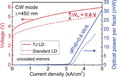
Fig. 2. L–I–V characteristics of standard LD (dashed lines) and TJ LD (solid lines). Both LDs operate in the CW mode at 450 nm.
Download figure:
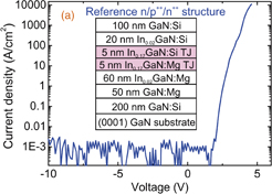
Standard image High-resolution imageTo investigate the TJ series resistance, we analyzed a simplified n/p++/n++ structure shown in the inset of Fig. 3(a) in order to reduce the impact of the different LD layers on the series resistance of the structure with the TJ. The samples were grown on Ga-polar HVPE GaN substrates and consisted of 200 nm n-type doped GaN:Si, 50 nm GaN:Mg, and 60 nm In0.02Ga0.98N:Mg doped at a level of 5 × 1019 cm−3, and a 10 nm In0.17Ga0.83N SQW. Above the SQW, 20 nm In0.02Ga0.98N:Si and 100 nm GaN:Si doped at a level of 3 × 1019 cm−3 are grown. We obtained the best results when the SQW region was heavily doped: first, 5 nm of the SQW was doped with Mg at a level of 1020 cm−3 and the next 5 nm of the SQW was doped with Si at a level of 5 × 1020 cm−3. The current–voltage (I–V) characteristics are shown in Fig. 3(a) for a processed sample with a mesa size of 30 × 30 µm2. The n/p++/n++ structure reaches a current density of 10 kA/cm2 at 4.55 V. Up to −10 V, no leakage has been observed because the n/p++ junction is in the reverse bias. Figure 3(b) shows the differential resistivity dU/dj vs the current density j. Our TJ design allowed us to achieve a differential resistivity lower than 10−4 Ω·cm2 for current densities higher than 2 kA/cm2, which is very promising for LD applications and is one of the best results among those reported in the literature.4,8,23,29)
Download figure:
Standard image High-resolution image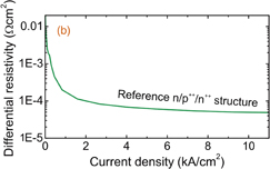
Fig. 3. (a) I–V characteristics of the n/p++/n++ test structure for 30 × 30 µm2 mesa. The figure inset shows the scheme of the n/p++/n++ test structure for the determination of series resistance. (b) Differential resistance versus current density.
Download figure:
Standard image High-resolution imageAn interesting remark can be given from the comparison of the differential resistivities of the standard LD, TJ LD, and test TJ n/p++/n++ structure. Figure 4 shows the differential resistivities of the standard PAMBE and TJ LDs (the I–V characteristics of which are depicted in Fig. 2). For the TJ LD, the resistivity is slightly higher, but there is no substantial increase in this value when compared with that of the standard LDs. For high current densities of 3–5 kA/cm2, the differential resistivity is at a level of 10−3 Ω·cm2, which is one order of magnitude higher than that of the test TJ n/p++/n++ structure. Moreover, the difference in differential resistivity between the TJ and standard LDs (marked with a red dashed line in Fig. 4) follows the differential resistivity of the test tunnel junction n/p++/n++ structure.

Fig. 4. Comparison of series resistances of the standard LD, TJ LD, and reference n/p++/n++ structure (solid lines). The dashed line shows the difference between the series resistances of the TJ LD and the standard LD.
Download figure:
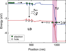
Standard image High-resolution imageThe main factor that decreases the wall-plug efficiency of TJ LDs is the increase in the operating voltage by 0.6 V. In Fig. 5, we present a band diagram of the TJ LD where this voltage drop is depicted. For the TJ LDs grown on (0001) GaN, the TJ operates in the reverse bias mode (Zener diode). The increase in LD operating voltage is related to the required polarization of the TJ for a high tunneling current density; a high applied voltage decreases the depletion region width. However, in the future, the increase in TJ LD operating voltage can be compensated partially by the reduction in the width and thus the resistance of the upper p-type part of the LDs. Additionally, a new design of the LDs with a metal contact deposited outside of the mesa will allow us to use air as a cladding and reduce the thickness of the p-type upper cladding, which in turn can substantially reduce the voltage on LDs. As demonstrated by Malinverni et al.,10) a 200 nm AlGaN:Mg cladding (instead of 500 nm) was sufficient to achieve good parameters of LDs.
Fig. 5. Band diagram of TJ LD. The voltage drop ΔV enables high-current-density tunneling through the TJ.
Download figure:
Standard image High-resolution image
In conclusion, we have demonstrated monolithic tunnel junction laser diodes grown by PAMBE operating in the CW mode at the wavelength λ of 450 nm. The application of TJs allows us to make n-type ohmic contacts for both device sides eliminating the problematic p-type contact. The absence of hydrogen during PAMBE growth allows us to achieve TJs with low resistance. The serial resistivity of the n/p++/n++ test structures was below 10−4 Ω·cm2 for current densities higher than 2 kA/cm2, while for TJ LDs, it was one order of magnitude higher. The lasing threshold current density and slope efficiency of TJ LDs were the same as those of the standard PAMBE LDs. The differential resistivities of TJ and standard LDs are in the same range, while the turn-on voltage increased for TJ LDs by 0.6 V. This result opens new perspectives for the growth of devices operating at high current densities such as VCSELs or cascades of laser diodes.
Acknowledgments
This work was supported partially by the Foundation for Polish Science (Grant No. TEAM TECH/2016-2/12) and the Polish National Centre for Research and Development (Grants Nos. PBS3/A3/23/2015 and LIDER/29/0185/L-7/15/NCBR/2016).