
Abstract
We report the first demonstration of III–nitride vertical-cavity surface-emitting lasers (VCSELs) with tunnel junction (TJ) intracavity contacts grown completely by metal–organic chemical vapor deposition (MOCVD). For the TJs, n++-GaN was grown on in-situ activated p++-GaN after buffered HF surface treatment. The electrical properties and epitaxial morphologies of the TJs were first investigated on TJ LED test samples. A VCSEL with a TJ intracavity contact showed a lasing wavelength of 408 nm, a threshold current of ∼15 mA (10 kA/cm2), a threshold voltage of 7.8 V, a maximum output power of 319 µW, and a differential efficiency of 0.28%.
Export citation and abstract BibTeX RIS

Content from this work may be used under the terms of the Creative Commons Attribution 4.0 license. Any further distribution of this work must maintain attribution to the author(s) and the title of the work, journal citation and DOI.
Vertical-cavity surface-emitting lasers (VCSELs) have been studied for their various advantages including small device size, low threshold current density, high modulation bandwidth, narrow linewidth, and circular beam shape.1–3) In particular, III–nitride VCSELs have attracted much interest owing to their unique emission wavelengths (ultraviolet to green) for attractive applications, such as visible light communication, optical sensors, displays, and atomic clocks.4–9) Reports of III–nitride VCSELs have consisted of hybrid epitaxial/dielectric10,11) and dual dielectric DBR designs.7–9,12–14) Both designs have required intracavity contacts, and indium tin oxide (ITO) has been the most commonly used material to improve lateral current spreading on the p-side. However, the high absorption loss of ITO can lead to significantly higher threshold currents and lower light outputs.8)
GaN tunnel junctions (TJs) with n-GaN layers are a promising alternative for p-contacts and current spreading.4,9,15,16) When a reverse bias is applied to the heavily doped p–n junction layer, electrons tunnel from the valence band to the conduction band.4) In addition to the highly doped n++-GaN in the TJ, a thicker n-GaN layer can be grown to improve current spreading and heat transfer while having lower optical loss than ITO and p-GaN.8,17) Furthermore, TJs offer more flexibility to design various structures, such as buried TJ current apertures and dual epitaxial DBRs, as demonstrated previously in GaAs- and InP-based VCSELs.1) Despite those benefits, metal–organic chemical vapor deposition (MOCVD)/molecular beam epitaxy (MBE) hybrid growth has been the only technique reported for GaN-based VCSELs with TJs.8) Growing the entire VCSEL epitaxial structure by MBE is not yet desirable because the relatively low growth temperature has resulted in higher concentrations of defects and impurities causing nonradiative recombination.18) Moreover, because MOCVD is better suited for the mass production of semiconductor devices, developing III–nitride VCSELs with TJs completely grown by MOCVD is highly desirable. However, these devices have not been reported thus far because of several physical and technical challenges.
One of the issues for MOCVD-grown TJs is Mg activation for a p-type layer buried by n-type layers. An n-GaN capping layer on a Mg-doped p-GaN layer behaves as a strong barrier to hydrogen diffusion and thereby prevents activation. Mg activation by sidewalls has been proposed;19,20) however, this method constrains the freedom of device design and size owing to the limited diffusion length of hydrogen. Moreover, hydrogen diffusion could also be limited by ion implantation, which has been widely used to form current apertures of GaN-based VCSELs.7–9,13) Thus, in-situ bulk p-GaN activation during TJ regrowth offers more flexibility in device design and can be applied to other devices, such as LEDs and edge-emitting lasers.
In this work, we demonstrate, for the first time, III–nitride VCSELs employing TJ contacts completely grown by MOCVD. LED test structures were first investigated to develop the in-situ p-GaN activation process for MOCVD-grown TJs. The epitaxial structure was grown in two steps to form the main LED structure that ends with p-type GaN and then the n-type GaN to form a TJ. The two-step growth (i.e., taking the samples out of the MOCVD chamber before current-spreading-layer growth) was necessary to define apertures by ion implantation for VCSELs before regrowth. This also enabled the use of a buffered HF (BHF) treatment on the p++-GaN surface prior to regrowth, which led to improved TJ contacts. Finally, we present violet VCSELs with GaN TJ intracavity contacts, dual dielectric DBRs, and ion implant apertures. A 14-µm-diameter-aperture VCSEL yielded a threshold current density of 10 kA/cm2, a peak output power of 319 µW, and a differential efficiency of 0.28%.
The LED test samples with TJ contact layers were grown by MOCVD on a bulk m-plane GaN substrate with an intentional −1° miscut in the c-direction to investigate TJ characteristics. The epitaxial structure consisted of a ∼1 µm n-GaN template, active multi-quantum wells (MQWs) (5 × QWs, 3 nm InGaN wells with 2 nm GaN barriers), 100 nm p-GaN, and a 10 nm p++-GaN contact layer. The wafer was then taken out of the reactor and cleaved into several pieces. Different activation conditions and surface treatments were carried out for each sample. One representative sample was treated in BHF for 5 min to remove a Mg-rich film on the surface of p++-GaN to reduce Mg diffusion into the sequentially regrown n++-GaN layer.19,21) During temperature ramp up to 900 °C for regrowth, the MOCVD chamber was held at 750 °C for 5 min to activate the p-GaN. The TJ structure consisted of 40 nm n++-GaN, 100 nm n-GaN, and 5 nm n+-GaN with a Si doping concentration of approximately 1 × 10²⁰, 1.8 × 10¹⁸, or 1 × 1019 cm−3. For electrical measurements, Ti/Au (20/500 nm) was deposited by electron-beam (e-beam) evaporation on the p-side. Then, ∼200 nm was etched to define circular mesas by reactive ion etching (RIE) using Ar/Cl2 plasma. The etching depth was chosen to minimize sidewall leakage, as well as to remove the current-spreading layer outside the mesa. For n-contacts, indium was soldered on the back of the substrates. The device structure of the TJ LED test samples is illustrated in Fig. 1.
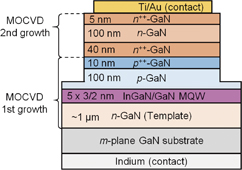
Fig. 1. Schematic of MOCVD-grown TJ LED test structure.
Download figure:
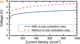
Standard image High-resolution imageAfter processing, the current density–voltage (J–V) characteristics in continuous waves (CWs) were measured up to a current density of 1 kA/cm2 for TJ LED test samples with different surface treatments prior to TJ regrowth and different activation conditions. As shown in Fig. 2(a), an in-situ activation step at 750 °C for 5 min resulted in a sharper turn on with a 1.1 V lower voltage at a current density of 1 kA/cm2 than for the sample without an in-situ activation step. However, the sample without the in-situ activation step was still partially activated during the ramp up to the regrowth temperature (900 °C). In addition, the TJ structure was grown on a preactivated sample in a furnace under our standard activation conditions (at 600 °C for 10 min in air) for comparison. It showed a similar J–V curve to the in-situ activated sample (<0.1 V difference at all current densities); thus, it is unlikely that longer activation times at 750 °C would improve TJ contacts. However, it is still possible that p-GaN could be passivated by hydrogen generated from ammonia during the TJ regrowth. Further studies are necessary to verify the activation efficiency of p-GaN during this process.
Download figure:
Standard image High-resolution image
Fig. 2. J–V characteristics measured under CW operation for 50-µm-radius circular LEDs with TJ contacts grown with and without (a) an extra holding step at 750 °C for 5 min (in-situ activation) during the ramp up for regrowth and (b) BHF surface treatment on p++-GaN before regrowth.
Download figure:
Standard image High-resolution imageFigure 2(b) shows the role of surface treatment in BHF prior to TJ regrowth. The sample treated in BHF before regrowth showed a reduction of 0.5 V at 1 kA/cm2. We believe that the BHF treatment improved the voltage by reducing Mg diffusion into the n++-GaN layer, which could compensate electron carriers required to form an abrupt junction.15,19,21) Finally, the best results were obtained from the sample treated in BHF with in-situ activation prior to TJ regrowth, which showed voltages of 3.4 V at 20 A/cm2 and 4.5 V at 1 kA/cm2. These J–V characteristics are reasonably close to those of a diode with the MOCVD-MBE hybrid TJ contacts reported by Young et al. (3.05 V at 20 A/cm2),15) but the voltage of the MOCVD TJ sample could be increased owing to structural differences, including poor n-contact on lightly doped n-GaN and extra resistance from the substrate.
The surface morphologies of the TJ LED test samples were measured by atomic force microscopy (AFM) after both the first and second growths, as shown in Fig. 3. The surface remained smooth (<1 nm RMS roughness) after TJ growth, which is necessary to reduce scattering loss for VCSELs.22)

Download figure:
Standard image High-resolution image
Fig. 3. Surface roughness of the LED TJ test samples (a) before and (b) after TJ regrowth. RMS roughness was (a) 158 and (b) 503 pm.
Download figure:
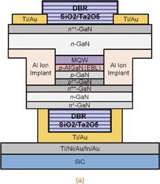
Standard image High-resolution imageNext, this method of in-situ p-GaN activation during MOCVD regrowth was applied to create VCSELs with MOCVD-grown TJ intracavity contacts, as shown in Fig. 4(a). The VCSEL structure was designed by simulating the optical mode intensity and index profile at a lasing wavelength of 410 nm, as shown in Fig. 4(b). The n++-GaN layer grown for TJ contacts was placed at a null of the mode to reduce internal loss. The top and bottom mirrors consisted of 17-period and 13-period distributed Bragg reflectors (DBRs) with simulated reflectance values of 99.9997 and 99.9938%, respectively. The simulation predicted that VCSELs have an internal loss (αi) of ∼12.61 cm−1, a mirror loss (αm) of ∼0.63 cm−1, a threshold material gain (gth) of ∼335 cm−1, and a cavity thickness of ∼6.38λ. Table I shows the estimated internal loss in each layer taking into account the optical absorption,8) thickness, and mode intensity. Approximately half of the total internal loss comes from the 759.4 nm n-GaN layer, and it can be reduced by decreasing the doping concentration and thickness, although conductivity and thermal impedance may increase.12)
Download figure:
Standard image High-resolution image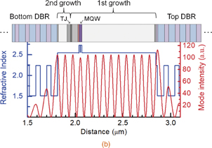
Fig. 4. (a) Schematic of the flip-chip VCSEL structure with dual dielectric DBRs and MOCVD-grown TJ contact and (b) cavity-mode intensity distribution overlaid with refractive index profile.
Download figure:
Standard image High-resolution imageTable I. VCSEL epitaxial layer structure grown on m-plane GaN substrate.8) (UID: unintentionally doped.)
| Epitaxial layer | Thickness (nm) | Doping concentration (cm−3) | Contribution to internal loss (%) |
|---|---|---|---|
| 2nd growth | |||
| n+-GaN | 10 | 1019 | 1.8 |
| n-GaN | 94 | 1.3 × 10¹⁸ | 6.0 |
| n++-GaN | 40 | 1020 | 9.4 |
| 1st growth | |||
| p++-GaN | 14 | 2.2 × 10²⁰ | 21.7 |
| p-GaN | 61.2 | 1019 | 12.8 |
| p-AlGaN | 5 | 2.2 × 10¹⁹ | 1.3 |
| 2 × InGaN/GaN MQW | 14/1 | UID | |
| n-GaN | 759.4 | 2.3 × 10¹⁸ | 45.7 |
| n+-GaN | 15 | 1.7 × 10¹⁹ | 1.3 |
| InGaN (sacrificial QW) | 7 | UID | |
| n-GaN (template) | ∼1300 | 1.3 × 10¹⁸ | |
For VCSEL processing, the main epitaxial structure was grown up to the p++-GaN contact layer and then followed by a mesa etch and Al ion implantation to form the current aperture. Ion implantation outside of the apertures was also used to prevent the lateral etching of the MQW by photo-electrochemical (PEC) etching during the flip-chip process in a later stage.23–25) Next, the MOCVD regrowth to form the TJ was performed after aqua regia and BHF treatments. TJ etching was then performed followed by the deposition of a 17-period Ta2O5/SiO2 DBR. After metal contact deposition, flip-chip bonding was carried out on a SiC substrate coated with Ti/Ni/Au/In/Au metals. The GaN substrate was then removed by PEC etching of a sacrificial QW. Finally, Ti/Au was deposited as the n-contact, followed by the deposition of a 13-period SiO2/Ta2O5 DBR with a 1/8th-wave Ta2O5 spacer next to n++-GaN. The detailed thicknesses and doping concentrations of the full epitaxial structure are shown in Table I.
After VCSEL fabrication, the optical and electrical characteristics of the VCSELs were studied. As shown in Fig. 5, the light–current–voltage (L–I–V) characteristics of the VCSEL were analyzed under pulsed operation with a pulse width of 300 ns and a duty cycle of 0.3% at room temperature. The threshold current density (Jth) and voltage (Vth) were 10 kA/cm2 and 7.8 V, respectively. The laser was measured up to a voltage of 12 V, which gave an output power of 319 µW at 55 kA/cm2. The differential efficiency (ηd) was 0.14% near Jth (20 kA/cm2) and increased to 0.28% at a high current density (50 kA/cm2). The kink in the L–I curve at ∼40 and ∼70 mA is likely due to the appearance of higher order lasing modes. In comparison to a VCSEL with a hybrid TJ8) and a similar structure (cavity thickness, ion-implanted aperture, epitaxial growth on m-plane, etc.), a similar voltage at low current density was achieved (∼7.0 V at 5 kA/cm2 for both devices).8) Similar to the case of previously reported hybrid TJs,8,15,16) we believe that the MOCVD-grown TJ led to an increase in the effective turn-on voltage. The differential resistivity was found to be 10−4 Ω cm2 at a current density of 20 kA/cm2, which is higher than that of the one with the hybrid TJ (∼5 × 10⁻⁵ Ω cm2). From the doping concentrations and mobilities,15) the sheet resistances of the top (p-side) and bottom (n-side) layers were calculated to be 165.7 and 116.5 Ω/sq, respectively. We believe that the low doping concentrations of the current-spreading layers on the p-side are the main cause of the high differential resistivity that limits the device performance. The emission spectrum in Fig. 5 shows the lasing wavelength of 408 nm with the full width at half maximum (FWHM) of 1.9 nm, which is limited by the resolution of the spectrometer.
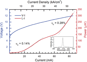
Fig. 5. L–I–V characteristics of a 14-µm-diameter-aperture VCSEL measured under pulsed operation at a duty cycle of 0.3% with a 300 ns pulse width. Inset exhibits electroluminescence (EL) spectrum at ∼20 mA.
Download figure:
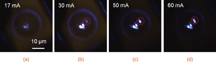
Standard image High-resolution imageAs shown in Fig. 6, near-field images of the VCSEL as a function of current were also taken. The increase in the number of lasing spots observed in Figs. 6(a) and 6(b) caused gradual increases in output power at low current (from 15 to 25 mA in Fig. 5). The onset of higher order modes from Figs. 6(b)–6(d) was also observed while the original spot remained the same. These changes in mode behavior could lead to kinks in the L–I curve, as mentioned above. This filamentary lasing, or unpredictable lasing spots at various currents and different lasing behaviors on each spot, has been reported in other III–nitride VCSELs.8,9) Such nonuniformity could be a result of various mechanisms, such as the nonuniformity of optical loss and current injection. In this device, we believe that the poor current-spreading layer and the variation of contact resistance in the TJ were the main causes, which were also shown in the I–V curve. Furthermore, surface residues after PEC etching, such as gallium oxide,12) could also be another issue. Improvements in the TJ contact and current-spreading layers will likely lead to improved lateral mode profiles and lower operation voltage.
Fig. 6. Optical microscopy images of a 14-µm-diameter-aperture VCSEL taken as a function of current above threshold current (∼15 mA). Exposure times of camera were the same for (a) and (b) and reduced for (c) and (d) to obtain clear images. Lasing spots in red circles show mode switching to higher order mode.
Download figure:
Standard image High-resolution image
In summary, we first analyzed in-situ p-GaN activation and surface treatments for TJs grown by MOCVD. The in-situ activation step at 750 °C for 5 min and the BHF surface treatment were effective to reduce the voltage by 1.1 and 0.5 V at 1 kA/cm2, respectively, on the TJ LED test samples. Finally, we demonstrated a GaN-based violet VCSEL with an in-situ activated MOCVD-grown TJ intracavity contact, dual dielectric DBRs, and an ion-implanted aperture. The VCSEL had a threshold current density of 10 kA/cm2, a peak output power of 319 µW, and a differential efficiency of 0.28%. Future improvements in the TJ and current-spreading layers may lead to lower operation voltages and eliminate the need for filamentary lasing.
Acknowledgments
This work was funded by the Solid State Lighting and Electronics Engineering Center (SSLEEC) of the University of California, Santa Barbara (UCSB). A portion of this work was carried out in the UCSB nanofabrication facility, UCSB Materials Research Laboratory (MRL), which is supported by the NSF MRSEC program (NSF DMR 1720256), and the California Nano System Institute's (CNSIs) Center for Scientific Computing at UCSB.