
Abstract
In today's highly information-oriented society, a continuously increasing number of computing devices are needed in the Internet-of-Things (IoT) era, from high-end servers in cloud to sensor node devices in edge. Under the constraint of power consumption, energy-efficient computing is necessary to enable low-power operation and implement emerging algorithms such as machine learning. A steep-subthreshold-slope (SS) transistor can be a next-generation device technology platform for highly energy-efficient computing. Among several types of steep-SS transistors, the negative-capacitance field-effect transistor (NCFET) has recently become one of the most promising candidates in terms of on-current, process integration, and cost, coincident with the discovery of ferroelectric HfO2. In this review paper, the concept and recent research studies on NCFET are reviewed. Technical challenges and future prospects are discussed.
Export citation and abstract BibTeX RIS
1. Introduction
In today's highly information-oriented society, the cyber physical system (CPS) has been an important business platform. Tremendous amounts of data are collected from real space. These data are stored and analyzed in cloud computing in virtual space. Then, new strategic social services are provided back to the real space. In CPS, an Internet-of-Things (IoT) edge device plays an important role as a sensor node device. The number of IoT devices will grow to be trillions or more; thus, the power consumption of an IoT device must be ultralow because of power constraints. From the economical viewpoint, battery maintenance and replacement for each IoT device will cost a lot. Therefore, ultimately, an IoT device should operate by generating and managing its own power with the use of energy harvesting techniques. The available power supply depends on the environment. For example, in a room environment, the available power may be as much as 1 µW from human vibration, environmental radio, and so on.1) However, a modern commercially available sensor node device consumes tens or hundreds of µW. Therefore, to realize an autonomous IoT device, power consumption should be reduced by more than tenfold from current levels. This challenge is addressed by introducing new integrated device technologies.
To illustrate the device technology that will be needed, first, the power consumption of a low-power microcontroller unit (MCU) is estimated. Figure 1 shows the power consumption of MCU versus the active rate, which represents the switching times of a transistor per second on average for different technologies and leakage currents. In this model, dynamic and static powers were calculated on the basis of commercial low-power MCUs2) and the SRAM cell current multiplied by the number of SRAM cells,3,4) respectively. At a high active rate, the active switching power is dominated, while at a low active rate, the standby leakage power is dominant. An IoT device is supposed to operate in an intermittent mode so that its active rate will be low. Therefore, the power consumption of an IoT device will be dominated by standby leakage power.

Fig. 1. Estimated power consumption of a low-power MCU with different technologies and transistor leakage currents.
Download figure:
Standard image High-resolution imageTo achieve power consumption at the µW or nW level, it is necessary to suppress leakage current by more than tenfold but maintain drive current and dynamic performance. The on-current–off-current ratio (Ion/Ioff) must be high. This can be achieved by reducing the subthreshold slope (SS). The SS of MOSFET5) is expressed by
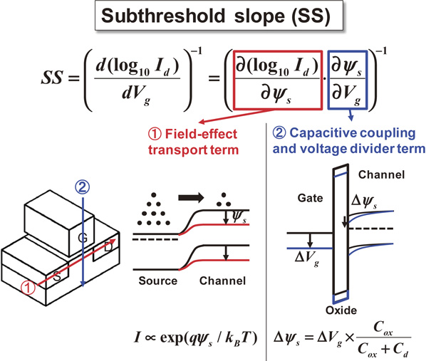
On the rightmost side, the first term represents how much the drain current (Id) can increase by bending the surface potential (ψs), which depends on the electron transport mechanism under a certain field effect, as illustrated in Fig. 2. The second term represents how much the surface potential can bend as the gate voltage (Vg) increases, which is determined by a voltage divider between the gate insulator and the substrate. There is a physical limit of SS in a conventional MOSFET. It is about 60 mV/dec at room temperature, which can be theoretically realized by assuming an ideal diffusion current from source to channel and an infinitely large gate-insulator capacitance. Because of the severe power requirement in the near future, the International Roadmap for Devices and Systems (IRDS) projects that SS will need to be 40 mV/dec by 2033,6) as shown in Fig. 3. A transistor with a steep SS enables energy-efficient switching.7) Therefore, the physical limit of 60 mV/dec must be overcome for the system requirement.8,9)

Fig. 2. Schematic illustration of the physics of SS. SS can be represented by two terms: field-effect transport term and voltage divider term.
Download figure:
Standard image High-resolution image
Fig. 3. Roadmap of SS projected by IRDS.6) GAA stands for gate-all-around.
Download figure:
Standard image High-resolution imageA sub-60 mV/dec SS can be theoretically achieved by engineering either the first or second term of Eq. (1). TFET10–13) and IMOS14,15) are examples that show a sub-60 mV/dec SS by engineering the first term, whereas the floating-body effect SOI transistor16,17) is one device that can engineer the second term. Currently, TFET is actively studied and an excellent steep SS has been achieved. However, there are several technical challenges on TFET: (1) relatively low Ion due to tunneling transport, (2) asymmetric operation between source and drain, and (3) complicated material and process requirements.
The negative-capacitance FET (NCFET) is an emerging transistor technology18,19) that can achieve a sub-60 mV/dec steep SS by engineering the second term. Together with the recent breakthrough in material development, NCFET has become one of the most promising steep-SS transistors with benefits of (1) high drive current due to conventional drift-diffusion transport, (2) symmetric operation between source and drain, and (3) low cost.
In this paper, recent studies of NCFET are widely overviewed. First, the original concept of NCFET is explained in Sect. 2. Then, recent research results are introduced in Sect. 3. Lastly, the latest findings are discussed in Sect. 4. Section 5 shows the summary.
2. Original concept of NCFET
NCFET was originally proposed by Salahuddin and Datta.18,19) The SS of a MOS transistor is simply expressed by using the gate insulator capacitance (Cox) and substrate capacitance (Cs),
To achieve sub-60 mV/dec, that is, SS < 60 mV/dec, the capacitances should satisfy the following conditions:

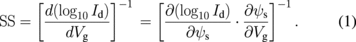
These conditions mean that Cox must be negative and Cs must be appropriately designed to be less than |Cox|. If such a negative-capacitance gate insulator is available in the field-effect transistor device in Fig. 4(a), a sub-60 mV/dec steep SS can be achieved according to the simulation result shown in Fig. 4(b).19) In this section, the physics of negative capacitance (NC) and the operation principle of NCFET are illustrated in the context of the original concept. The important concept of capacitance matching is discussed. The early NCFET works are introduced.

Fig. 4. (a) Schematic of NCFET, the gate insulator of which is a FE material. (b) Simulated Id–Vg characteristics of NCFET as well as 45 nm conventional MOSFET for reference. (c) (i) and (ii) show free-energy U versus charge of FE and PE, respectively. (iii) and (iv) show V versus Q of FE and PE, respectively. V is obtained by taking the derivative of U with respect to Q. Reprinted with permission from Ref. 19. © 2018 IEEE.
Download figure:
Standard image High-resolution image2.1. Negative capacitance
NC cannot be seen in a typical paraelectric (PE) gate insulator, but it can be seen in a ferroelectric (FE) gate insulator, as shown in Fig. 4(c).19) NC in FE can be derived from phenomenological Landau free energy.20) Suppose you have a single-domain FE material. The space inversion symmetry is broken in FE materials. This leads to double-well free energy, which is described by the Landau free energy, as a function of the order parameter of charge Q [Fig. 4(c)-(i)], while PE has a single obvious energy minimum [Fig. 4(c)-(ii)]. Conventionally, Q in FE represents spontaneous polarization (P). If you take a derivative of the free energy of a FE capacitor connected with a power supply by an order parameter, you can obtain the force field voltage V. This Q–V curve corresponds to the P–V curve, which can be extracted from the Q–V curve measured in a FE capacitor as a hysteretic curve where remanent polarization (Pr) and coercive field (Ec) are characteristic quantities. If you take a derivative of Q by V, you can obtain the capacitance C as a coefficient to relate order parameter Q to force field V. Capacitance is positive for a PE capacitor [Fig. 4(c)-(iv)], whereas it can be negative for a FE capacitor in a certain voltage range [Fig. 4(c)-(iii)].
However, the NC effect is available only in the metastable state of the Landau free energy with a negative curvature, which is not stable with the FE capacitor itself. To utilize the NC effect in stable condition, the PE capacitor should be connected in series.18,19) If an appropriate PE capacitor is connected to the FE capacitor, the total free energy can be minimized, while NC is accessible in the FE capacitor, as illustrated in Fig. 5,21) which shows the transition of the energy of the FE capacitor (UFE) and the total energy of the series-connected capacitor (Utot) as Vg increases. The FET substrate capacitance can include an interfacial oxide capacitor in series and works as a matching capacitor to the FE capacitor. Capacitance matching will be explained later.

Fig. 5. (Top) Calculated energies of FE capacitor (UFE) and (bottom) total energies of series-connected FE and PE capacitor (Utot) from zero Vg (left) to high Vg (right) bias.
Download figure:
Standard image High-resolution image2.2. Operation principle
NCFET is almost the same as a conventional MOSFET except that the gate insulator is FE, as shown in Fig. 4(a). In this section, the operation principle of NCFET based on the original concept18,19) is explained in the form of a simple bulk FET without interfacial oxide.22) Assume that the flat-band voltage is zero. Considering charge neutrality, the polarization charge matches the substrate charge. Therefore, when you draw a P–V curve for FE and the substrate charge versus voltage curve for FET in the same graph, the cross-point represents the operation point of NCFET. These operation point and corresponding band diagrams are shown in Fig. 6. As Vg is applied, the curve for FET moves to the right and thus the operation point moves [Fig. 6(a)]. As a large Vg is applied, a more negative voltage is induced on the FE gate insulator so that the surface potential becomes larger than the applied Vg, ∂ψs/∂Vg > 1 [Fig. 6(b)]. This is the so-called voltage amplification. Since the transport mechanism of NCFET is just the same as that of MOSFET, i.e., drift and diffusion, the SS of NCFET can be less than 60 mV/dec at room temperature according to Eq. (1). Note that, once a sufficiently large Vg is applied and the operation point moves away from the NC region in the P–V curve, a positive voltage is applied to the FE gate insulator and ψs cannot exceed Vg anymore [Fig. 6(c)]. Mathematically, there will be no hysteresis, the operation is reversible, and the voltage across FE (Vfe) does not need to exceed the coercive voltage (Vc) of FE, as long as Cox < 0 and |Cox| > Cs are satisfied. If Cox < 0 but |Cox| < Cs, a steep SS can still be obtained but with hysteresis having bistable operation points.

Fig. 6. (Top) Operation points in P–V curves as a cross point with FET load line and (bottom) corresponding schematic band diagrams of NCFET. (a) A negative voltage is induced on the gate insulator, and then (b) the surface potential is amplified at a higher gate bias. (c) At a sufficiently high Vg, a positive voltage is induced on the gate insulator.
Download figure:
Standard image High-resolution image2.3. Capacitance matching
Now that the FET substrate capacitance works as a matching capacitor to the FE capacitor, the substrate capacitance needs to be appropriately designed to satisfy |Cox| > Cs. Capacitance matching23–25) can be done (1) by adjusting the FE material to the fixed substrate of FET and/or (2) by adjusting the substrate of FET to the fixed FE material. In case (1), a general guideline to realize a steep SS is that the P–V curve should be compressed, meaning that Pr should be small and Ec should be large so as to make the NC slope in the P–V curve close to that of FET. In case (2), the substrate capacitance, which typically consists of the interfacial oxide and channel capacitances, should be sufficiently large to match the capacitance of the FE gate insulator. This is important because the channel capacitance in the subthreshold region is very small owing to the low density and low capacitance of the space charge in the depletion layer. Channel design for capacitance matching will be discussed later. To design and realize capacitance matching, some matching curves are used in hand. For example, drawing the Q–V curves of the FE and FET substrate as shown in Fig. 723) is useful for visualizing how closely the capacitances and charges of the FE and FET substrate match.
Download figure:
Standard image High-resolution image
Fig. 7. (a) Schematic of an NCFET and its capacitor network model, which consists of FE and MOS capacitors with source and drain. (b) Calculated Q–V curves of FE and MOS capacitors in NCFET. This graph is called a matching curve. Reprinted with permission from Ref. 23. © 2018 IEEE.
Download figure:
Standard image High-resolution image2.4. Experimental evidence of negative capacitance
There are several reports that experimentally observed NC in the context of the original concept of NCFET. The NC effect was observed in a series-connected FE capacitor and a paraelectric (DE) capacitor in high-frequency C–V measurement26,27) as shown in Fig. 8.26) Generally, the series-connected capacitance becomes smaller than that of an individual capacitor. However, the FE capacitance rather enhances the DE capacitance by series connection [Fig. 8(c)], which is consistent with the simulation result [Fig. 8(b)].

Download figure:
Standard image High-resolution image
Download figure:
Standard image High-resolution image
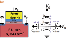
Fig. 8. (a) Schematic of a bilayer capacitor of FE and paraelectric (DE). PZT, STO, and SRO stand for Pb(Zr,Ti)O3, SrTiO3, and SrRuO3, respectively. (b) Simulated C–V curves of bilayer and single DE capacitors. (c) Measured C–V curves of bilayer and single DE capacitors as a function of temperature. Reprinted with permission from Ref. 26. © 2018 AIP publishing.
Download figure:
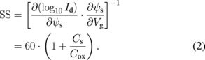
Standard image High-resolution imageThe NC effect was also observed by using the transient measurements28) shown in Figs. 9(a) and 9(b). The motivation to use transient measurements is that, if you sweep the external voltage applied to the FE capacitor, you can only observe the monotonic increase in P as a function of V29) and you will neither access the NC region in the P–V curve nor observe the NC effect. Instead of the sweeping voltage, you can sweep the charge by using a transient system. Having resistance in series, you can regulate the current and control the charge, and then measure the voltage induced on the FE capacitor. Q is calculated by integrating the measured current, and the Q–V curve of FE can be reconstructed. Although it is not possible to fully trace the S-shape NC region, the NC effect can be observed as a voltage snapback in the measured Q–V curve of FE, as shown in Fig. 9(c).28)
Fig. 9. (a) Schematic of transient measurement of FE capacitor connected with series resistor. PVDF stands for polyvinylidene fluoride. P(VDF-TrFE) is a copolymer with trifluoroethylene (TrFE), which shows ferroelectricity. (b) Schematic circuit diagram corresponding to (a). (c) Current, charge, and voltage in FE capacitor can be measured and extracted from (b). The P–V curve can be reconstructed from these data by plotting the measured charge versus the measured voltage. Reprinted with permission from Ref. 28. © 2018 Springer Nature.
Download figure:
Standard image High-resolution image2.5. Early NCFET works
Steep SS characteristics were already observed back in 2008–2010.30,31) For example, a metal–FE-metal–insulator–semiconductor (MFMIS)-FET was fabricated by using a conventional FE material. MFMIS-FET can be seen as the device that integrates the MFM capacitor and MISFET on the same device. The MFMIS structure is useful because the internal node voltage can be monitored to observe voltage amplification. The top MFM capacitor and bottom MISFET can be independently characterized as well. By fabricating the device shown in Fig. 10(a), a sub-60 mV/dec SS was observed30,31) in Fig. 10(b).31) In another paper, the authors came up with the idea of connecting a discrete transistor and a FE capacitor on different chips by wire bonding, as shown in Fig. 10(c).32) Their paper also showed a sub-60 mV/dec SS with a surprisingly small hysteresis [Fig. 10(d)].

Fig. 10. (a) Schematic of NCFET as metal–ferroelectric–metal–insulator–semiconductor (MFMIS)-FET with internal metal gate, which serves to monitor internal node voltage. (b) Measured SS values of three different devices, which have the structure of (a) with different sizes. (a) and (b) are reprinted with permission from Ref. 31. © 2018 IEEE. (c) An MFMIS-type NCFET is implemented by wiring a discrete MOSFET sample and a FE capacitor sample. (d) Measured Id–Vg curves of the MFMIS-FET and discrete MOSFET shown in (c). (c) and (d) are reprinted with permission from Ref. 32. © 2018 IEEE.
Download figure:
Standard image High-resolution image3. Recent research studies of NCFET
Until recently, NCFET did not attract much attention because it uses the FE gate insulator and it was difficult to find a FE material compatible with the CMOS process. However, there was a material breakthrough; ferroelectricity was discovered in a HfO2 film, which is a mature technology as a high-k gate dielectric in the CMOS process. Because of this breakthrough, NCFET has now become one of the most promising steep-slope transistors. In this section, FE-HfO2 is briefly introduced. The design of NCFET with FE-HfO2 is explained. Recent reports of sub-60 mV/dec SS are introduced. Then, several design options and considerations for NCFET are discussed.
3.1. Material breakthrough: FE-HfO2
It is known that crystallized HfO2 shows a higher dielectric constant than amorphous HfO2. There were studies on utilizing crystallized HfO2 as a next-generation high-k gate dielectric for CMOS process integration.33) In the course of developing such a high-k gate dielectric for either logic or DRAM application, ferroelectricity has been discovered in a HfO2 thin film.34,35) Figure 11(a) shows an example of sub-10 nm FE-HfO2. By doping with Si, Al, or Zr, and with an appropriate metal electrode and annealing conditions, crystallized HfO2 shows ferroelectricity. HfZrO2 is a popular FE-HfO2 material that shows ferroelectricity and anti-ferroelectricity depending on the Zr concentration. Typically, an orthorhombic phase appears in a FE-HfO2 thin film. Unlike a conventional perovskite material, the displacement of an oxygen anion instead of a metal cation is considered to be the origin of ferroelectricity.36,37)

Download figure:
Standard image High-resolution image
Fig. 11. (a) Cross-sectional TEM image of 9-nm-thick HfO2–ZrO2 film with top and bottom TiN electrodes. (b) Measured P–V and dielectric constant versus V characteristics of HfO2–ZrO2 capacitors with different composition ratios of HfO2 and ZrO2. Reprinted with permission from Ref. 35. © 2018 American Chemical Society.
Download figure:
Standard image High-resolution imageThere are several advantages in FE-HfO2. Ferroelectricity can be seen in a sub-10-nm-thick HfO2 thin film35) without causing much leakage current due to a wide band gap. FE-HfO2 has a large Ec, and thus the memory window is large even with a very thin film. This means that FE-HfO2 is highly scalable and suitable for high-density logic and memory applications. FE-HfO2 is thermally stable between 600 and 1000 °C depending on the dopant.38,39) FE-HfO2 is compatible with the back-end H2 annealing process.40) Moreover, FE-HfO2 can be realized using standard CMOS-compatible metal electrodes such as TiN and TaN, which facilitate the patterning of a metal gate and a back-end interconnect.41) Therefore, FE-HfO2 is regarded as the most suitable gate insulator for NCFET.
Similarly to the method explained in Sect. 2.4, the NC effect has been observed by transient characterization,42,43) as shown in Fig. 12.42) Instead of by sweeping voltage across FE-HfO2, by regulating the current through the capacitor and obtaining the voltage across the capacitor, NC was observed in FE-HfO2 as a voltage snapback in the measured Q–V curve of FE-HfO2. Here, note that the observed NC effect in Figs. 9 and 12 can be explained by an alternative model instead of the original NC model based on Landau free energy, which will be discussed later.

Fig. 12. Measured P–V curve of FE-HfO2, which is reconstructed from measured current, charge, and voltage in FE-HfO2 by transient measurement, in the same way as Fig. 9. Reprinted with permission from Ref. 42. © 2018 IEEE.
Download figure:
Standard image High-resolution image3.2. NCFET with FE-HfO2
Thanks to the discovery of FE-HfO2, NCFET has become one of the most promising steep-SS transistors because of (1) high Ion/Ioff with high Ion, (2) CMOS-compatible material and process, and (3) minimum circuit design modification owing to the symmetric device structure and operation. The NCFET design was explored and a growing number of papers have demonstrated a sub-60 mV/dec steep SS.
3.2.1. Device design.
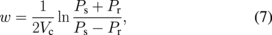
NCFET is designed on the basis of the material parameters of FE-HfO2, which are available for various material and process conditions. The FE-HfO2 thickness and channel structure are also options for design. These parameters should be optimized to satisfy capacitance matching. For future ultralow-power technologies, the target supply voltage (Vdd) will be less than 0.6 V.6) The model of NCFET can be built as a combination of a FE capacitor and a FET channel.19,23,44–46) Some open sources are also available.47) The FE capacitor can be analytically modeled by the Landau–Khalatnikov equation48) and the FET channel can be modeled by an analytical equation, SPICE model, or TCAD. The Landau–Khalatnikov equation is expressed as

Here, ρ is the switching resistivity that determines the dynamic response of the polarization in the FE material, G is the Landau free energy, and α, β, and γ are the Landau parameters that determine the static property of the FE material.
As a design sample, Fig. 13(a) shows the contour plot of Ion/Ioff for a HfO2-based NCFET as a function of the material parameters Pr and Ec. A design space exists where NCFET shows a higher Ion/Ioff than a conventional MOSFET even at Vdd = 0.2 V.49) A smaller Pr is preferred for charge matching between the FE and the FET channel, while Ec should be adjusted to avoid hysteresis. With a standard FET channel design, the material parameters can be chosen from the existing reported values of FE-HfO2 for Ion/Ioff, as shown in Fig. 13(b).22)

Download figure:
Standard image High-resolution image
Fig. 13. Simulated Ion/Ioff contour plot of NCFET as a function of Pr and Ec. The SS contour plot is also plotted on the same graph. Representative design points are indicated by dots. (b) Survey results of material parameters Pr and Ec of FE-HfO2 previously reported. Reprinted with permission from Ref. 22. © 2018 AIP Publishing.
Download figure:
Standard image High-resolution image3.2.2. Experimental demonstration of sub-60 mV/dec steep SS.
Since 2015, there have been a number of papers that demonstrated a sub-60 mV/dec steep SS in NCFETs with FE-HfO2.50–61) Here are some examples. In 2015, with 5 nm FE HfZrO2, a sub-60 mV/dec steep SS was observed in NCFET with a bulk Si FET channel as well as a Ge channel.50) Hysteresis in Id–Vg characteristics is as small as ∼0.1 V. NCFET was also fabricated with HfZrO2 and a bulk FinFET channel.51) Performance enhancement was clearly observed in both NFET and PFET. In 2016, FE HfZrO2 was scaled down to sub-2 nm, and a sub-60 mV/dec steep SS was clearly observed without hysteresis at all.52) A hysteresis-free NCFET was also demonstrated with a Ge channel.53) In 2017, FE HfAlO2 was employed for NCFET. The potential benefit of HfAlO2 is that it can endure a higher thermal budget, which may be required for reliability improvement. Again, a hysteresis-free sub-60 mV/dec steep SS was observed in NCFET with HfAlO2.54,55)
Figures 14(a) and 14(b) show representative data obtained from the measured Id–Vg curves of an n-type NCFET30,31,54–61) for forward and backward Vg sweeps, respectively, as well as a reference 14 nm CMOS.62) Figures 15(a) and 15(b) show the SS extracted from the measured Id–Vg curves in Figs. 14(a) and 14(b), respectively. Most of the devices show a sub-60 mV/dec steep SS in the range of more than 2 orders of magnitude of deep subthreshold current.

Download figure:
Standard image High-resolution image
Fig. 14. Benchmark of measured Id–Vg characteristics of previously reported n-type NCFETs for (a) forward and (b) backward sweeps. To avoid congestion in the graph, data are chosen such that (1) a steep SS was observed at more than 1–2 orders of magnitude, (2) the hysteresis was smaller than 0.1 V, (3) the subthreshold region is in the range between Vg = −1 and 1 V, and (4) FE-HfO2 was used, except in early studies.30,31)
Download figure:
Standard image High-resolution image
Download figure:
Standard image High-resolution image
Fig. 15. Benchmark of SS values of previously reported NCFETs extracted from Fig. 14 for (a) forward and (b) backward sweeps.
Download figure:
Standard image High-resolution image3.3. Options for device integration
3.3.1. Gate stack structure: MFIS versus MFMIS.
When exploring NCFET, there are two major architectures: MFIS and MFMIS. MFIS stands for metal-FE-insulator-semiconductor and MFMIS stands for metal–FE-metal–insulator–semiconductor. The only difference is whether the structure has an internal metal or not, as shown in Fig. 16(a),63) where MFIS and MFMIS are shown in (i) and (ii), respectively. As introduced in Sect. 2.5, early NCFET studies often used MFMIS. For MFMIS-FET, the MFM capacitor and MISFET can be independently designed and fabricated. Moreover, the internal node voltage can be directly measured, which is valuable information to confirm voltage amplification. However, if NCFET is considered to be introduced to advanced CMOS technologies that employ the replacement gate process with the sub-20 nm gate length,62) there will be no space to fill the gate trench with an internal metal. Moreover, the internal metal allows charge injection and accumulation, which prevent the expected NCFET operation. Therefore, MFIS-FET is the viable choice, although it is not possible to independently design and characterize the FE and FET channel.

Fig. 16. (a) Simulated contour plot of electrostatic potential of NCFET (i) without and (ii) with internal metal. The arrows show electric field vectors. (a) is reprinted with permission from Ref. 63. © 2018 IEEE. (b) Simulated Id–Vg curve of NCFET with and without internal metal. (c) Simulated (i) SS of NCFET versus Id and (ii) Ion/Ioff of NCFET without internal metal for different Kp values, with internal metal, and standard MOSFET. Kp represents the strength of the interaction of FE domains. (d) Simulated (i) DIBL and (ii) output resistance of NCFET without internal metal for different Kp values, with internal metal, and standard MOSFET. (b)–(d) are reprinted with permission from Ref. 65. © 2018 IEEE.
Download figure:
Standard image High-resolution imageFrom the device operation viewpoint, there is a distinct difference between MFIS and MFMIS in terms of the distribution of polarization in domains along the channel direction under drain-to-source bias (Vds).63–65) MFMIS has an internal metal where the potential is uniform. Since the potential difference between the top electrode and the internal metal is uniform along the channel, the polarization of the FE layer is uniform along the channel. Thus, surface potential can be amplified in nearly the entire channel region. On the other hand, MFIS does not have the internal metal so that the polarization of FE is not uniform along the channel. Thus, surface potential can be amplified mostly near the source region. The simulation work was performed by modeling the multidomain as a one-dimensional domain array with domain interaction.65) The work revealed that, if there is no gate leakage or charge injection to the internal metal, MFMIS is superior to MFIS in terms of subthreshold characteristics. The sub-60 mV/dec steep SS and high Ion/Ioff can still be achieved with MFIS as long as the domain interaction is sufficiently strong, as shown in Figs. 16(b) and 16(c).65) A negative DIBL and a negative differential resistance can be also observed in MFMIS and MFIS with a strong domain interaction, as shown in Fig. 16(d), which will be revisited later. There are several experimental studies on the difference between MFIS and MFMIS, which support the simulation result.57,58)
3.3.2. Channel engineering: 2D versus 3D.
In Sect. 2.3, the importance of capacitance matching is explained. With fixed material parameters for the FE layer, the substrate capacitance should be designed so as to satisfy the capacitance matching condition. In general, the substrate charge and capacitance in the deep subthreshold region are relatively much smaller than those of FE for bulk FET. Although FinFET is the current standard transistor, the channel region is fully depleted, and the charge and capacitance of the substrate are small. Therefore, it is relatively difficult to achieve charge and capacitance matching with the fin channel and FE gate insulator. On the other hand, a planar SOI transistor has a better chance of capacitance matching. If the SOI and BOX layers are thinned down with the bottom substrate highly doped, the substrate capacitance becomes relatively large even in the subthreshold region. The simulation study demonstrated that a thin body and a thin BOX SOI NCFET [Fig. 17(a)-(i)] can achieve a steeper SS than a fin NCFET [Fig. 17(b)-(ii)] with the fixed FE parameters and smaller BOX thickness, as shown in Figs. 17(b) and 17(c).66) This is mainly because the SOI NCFET has a larger substrate capacitance with a thin BOX and better capacitance matching. Thus, the NC effect is beneficial to mature planar SOI transistor technologies, and an ultralow-power NCFET can be realized by a low-cost process. There is an extra benefit for the thin SOI and BOX transistors, which is substrate biasing.67,68) Since such thin SOI and BOX structures allow strong substrate coupling, body capacitance can be tuned by substrate bias, which opens a wider design space.69) In NCFET, the substrate bias effect on threshold voltage (Vth) can be opposite to that in conventional MOSFET depending on the FE layer thickness and capacitance matching, as shown in Figs. 17(d) and 17(e),69) which provides an additional option for device design. Moreover, NCFET has also been experimentally demonstrated with 2D materials such as MoS2 with a clear sub-60 mV/dec steep SS.57,60,70) This indicates that the NC effect is not dependent on the substrate material or structure; rather, the NC effect can be used as a performance booster.

Fig. 17. (a) Schematic of device structures of (i) planar SOI NCFET and (ii) SOI NC FinFET. SOI and BOX stand for silicon-on-insulator and buried oxide, respectively. (b) Simulated Id–Vg characteristics of SOI NCFET and reference MOSFET with different BOX thicknesses. (c) SS versus BOX thickness for SOI NCFET and NC FinFET. (a)–(c) are reprinted with permission from Ref. 66. © 2018 The Japan Society of Applied Physics. (d) Schematic of thin body SOI FET with 2D channel material. (e) Simulated Vth of SOI NCFET with thin body and thin BOX versus Vbs as a function of FE layer thickness. (d, e) are reprinted with permission from Ref. 69. © 2018 IEEE.
Download figure:
Standard image High-resolution image3.3.3. Negative capacitance as a performance booster.
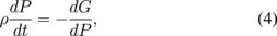
As mentioned in the last subsection, the NC effect can be an additive performance booster on any kind of charge-based field-effect transistor device. Moreover, it is possible to combine the NC effect with other steep-SS transistors such as TFET. Thus far, each type of steep-SS transistor has been independently studied by engineering each term in Eq. (1). If both terms in Eq. (1) can be engineered by synthesizing different types of steep-SS transistors, a supersteep-SS transistor can be realized. Therefore, combining TFET and the NC effect in the same device has been proposed.71,72) Although TFET utilizes tunneling transport, it still relies on the field effect for band bending. The NC TFET was designed on the basis of the vertical TFET with a FE gate insulator. The vertical TFET has a highly doped p–n junction on the source side under the gate, which facilitates the charge and capacitance matching in the deep subthreshold region. In fact, the simulation demonstrates that the NC TFET can better improve SS than TFET by more than 4 orders of the current level, as shown in Fig. 18(a).72) Energy efficiency, which is energy per switching, is greatly improved in Fig. 18(b). Recently, the NC TFET has been experimentally demonstrated in the device shown in Fig. 18(c), where on-current and SS are significantly improved as shown in Figs. 18(d) and 18(e), respectively.73) The NC effect proves to be an additive performance booster, which is a very important property as persistent technology for many generations.
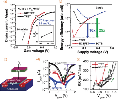
Fig. 18. (a) Comparison of simulated Id–Vg characteristics of NCTFET with those of conventional TFET. TFET stands for tunnel FET. (b) Simulated energy per switching, which is energy efficiency, for NCTFET compared with those for conventional TFET and SOTB transistor. (c) Schematic of NCTFET, which consists of discrete FE capacitor and Si TFET. (d) Measured Id–Vg characteristics and (e) SS of NCTFET illustrated in (c) and reference TFET. (a, b) and (c)–(e) are reprinted with permission from Refs. 72 and 73, respectively. © 2018 IEEE.
Download figure:
Standard image High-resolution image3.4. Device considerations
NCFET is expected to be a promising steep-SS transistor with an appropriate design as explained in Sect. 3.2.1, and a steep SS has indeed been experimentally observed, as mentioned in Sect. 3.2.2. However, there are several device considerations to bring NCFET to manufacturable CMOS technologies and practical applications. In this section, operation speed, device scalability, short-channel effect, reliability, and variability are discussed.
3.4.1. Operation speed.
From the original concept of NCFET, the latter should be able to drive a higher static Ion at a lower Vdd. In other words, energy-efficient switching is possible in the NCFET CMOS circuit. In fact, circuit simulation with the NCFET transistor model showed faster ring oscillator operation at lower power and Vdd.74) However, it is known that ferroelectricity originates from ionic displacement and domain dynamics.75–80) Because of the dynamics of charged ions and domains, the frequency range in which the polarization in FE can respond to is limited to microwave frequency. Compared with the standard MOSFET that uses the PE gate insulator with electronic displacement, the operation speed of NCFET may be limited to a lower frequency by the dynamics of polarization in the FE gate insulator instead of CV/I estimated from the static Ion. Therefore, it is important to model the dynamic characteristics of NCFET and predict the performance limit.42,81–84) The dynamic characteristics of NCFET are modeled by the Landau–Khalatnikov equation [Eqs. (4) and (5)]. ρ is the dynamic parameter representing switching resistance. ρ can be extracted from the transient measurement of the FE capacitor connected to known resistance in series, as shown in Fig. 19(a), and fitting the transient model to experimental results, as shown in Fig. 19(b).42) A multidomain is also implemented in the model by considering domain interaction energy.81) The static NCFET model can be extended to a dynamic one by including the dynamic term of dP/dt. The Id–Vg characteristics of NCFET were obtained by modeling and simulation with the extracted ρ value as shown in Fig. 19(c). The operation frequency of NCFET without causing a very large hysteresis can be on the order of >1–10 MHz range, as shown in Fig. 19(d),42) which may be suitable for low-speed but ultralow-power applications such as IoT edge devices. There are some experimental studies on the operation speed of NCFET,52,58) which indicates that NCFET shows a larger hysteresis at a higher Vg sweep rate even though quasi-static measurement shows nonhysteresis Id–Vg curves, which verifies the dynamic NCFET model mentioned above. For high-speed applications such as that in the GHz range, ρ needs to be orders of magnitude smaller. Thus far, the sample size in the transient measurement is quite large (on the order of microns). To accurately characterize a higher frequency response of polarization and extract intrinsic dynamic parameters to estimate operation speed, the measurement of the nanoscale FE capacitor without being limited by RC delay will be needed. Sub-µs polarization switching has been observed by careful measurement80) for a PZT material. Sub-µs polarization switching has also been observed in HfO2-based FeFET memory, as shown in Fig. 20(a). A 10–100 ns program and erase operation has been demonstrated, as shown in Figs. 20(b) and 20(c).85)

Fig. 19. (a) Schematic of transient measurement circuit of FE-HfO2 capacitor, where resistor is connected to FE capacitor. Current through the FE capacitor is monitored. The charge of the FE capacitor is calculated by integrating current. Voltage is calculated by subtracting the voltage drop of the resistor from the applied voltage. (b) Measured current waveform and current waveform simulated using a multidomain model with nearest-neighbor domain interaction. (c) (Left) Simulated Ψs and (right) Id versus Vg for different Vg sweep frequencies using ρ extracted by fitting in (b). (d) Extracted voltage hysteresis in Id–Vg curves in (c) with varying dynamic parameter ρ. Reprinted with permission from Ref. 42. © 2018 IEEE.
Download figure:
Standard image High-resolution image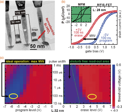
Fig. 20. (a) Cross-sectional TEM image of a 28 nm FeFET. (b) Measured Id–Vg curves of FeFET after erase and program pulses. (c) Measured memory window map of FeFET as a function of pulse width and erase/program voltage level. Reprinted with permission from Ref. 85. © 2018 IEEE.
Download figure:
Standard image High-resolution image3.4.2. Device scalability.
If the NC effect is to be employed in advanced CMOS technology, the process integration scheme must be taken into account. The current CMOS technology uses the FinFET architecture with the gate-last replacement-gate (RMG) process.62,86) In the RMG scheme, a dummy polygate is pulled out after source and drain formation, and interlayer dielectric deposition and planarization. Then, the gate trench is filled with a high-k gate dielectric, a metal gate to control the work function, and a low-resistivity interconnect metal. The gate trench width becomes less than 20 nm, which is very small. It is unknown if the NC gate stack can be filled in such a narrow gate trench and if there is any design space. Then, the NC FinFET was modeled and simulated in the structure shown in Fig. 21(a). The design sample is shown in the contour plot of Ion/Ioff in Fig. 21(b). Owing to the property of FE-HfO2, there exists a design space with practical material parameters and thickness for a higher Ion/Ioff in the NC FinFET than in the conventional FinFET, even at Vdd = 0.2 V.87) Theoretically, the NC FinFET can be scaled down to a gate length (Lg) less than 10 nm. The NC nanowire FET was also modeled and simulated in the structure shown in Fig. 21(c), and a similar conclusion was obtained with a tight pitch nanowire, as shown in Fig. 21(d).88)

Fig. 21. (a) Schematic of a double-gate NC FinFET with replacement gate scheme for simulation. (b) Simulated contour plot of Ion/Ioff of NC FinFET as a function of interfacial layer (Tox) thickness and FE layer thickness (Tfe). The design constraint by Lg is drawn by dotted lines. (a, b) are reprinted with permission from Ref. 87. © 2018 The Japan Society of Applied Physics. (c) Schematic of a gate-all-around nanowire NCFET for simulation with tight nanowire pitch. R is the radius of the nanowire. (d) Simulated contour plot of Ion/Ioff of nanowire NCFET as a function of nanowire diameter (2R) and Tfe. The design constraint by the nanowire pitch is drawn by dotted lines. (c, d) are reprinted with permission from Ref. 88. © Elsevier.
Download figure:
Standard image High-resolution image3.4.3. Short-channel effect.
When it comes to device scalability, the short-channel effect (SCE) must be addressed. In advanced CMOS technology, SCE becomes severe as Lg is scaled down. The pace of Lg scaling becomes slow at around 20 nm.89) It is important to understand how the NC effect has an impact on SCE in a scaled transistor. Theoretical studies revealed very interesting characteristics in the short-channel NCFET.63,90) In the short-channel NCFET, capacitance matching becomes intricate because parasitic capacitances and drain coupling are involved. However, this situation turns out favorable for capacitance matching and obtaining a steep SS. In fact, a short Lg NCFET shows a steeper SS than a short Lg conventional MOSFET, as shown in Figs. 22(a) and 22(b)-(i).63,90) Moreover, the SS of NCFET can be improved as Lg is scaled down. This is because a relatively larger parasitic capacitance than the substrate capacitance facilitates capacitance matching in the subthreshold region. In addition, the Lg dependence on the Vth and DIBL of NCFET is different from that of the conventional MOSFET, as shown in Fig. 22(b)-(ii). At a small Lg, while the conventional MOSFET shows Vth roll-off and a positive DIBL, the NCFET shows Vth roll-up and a negative DIBL.63,90) The reason for the Vth roll-up is that, for the same Ψs under the threshold condition, less charge is induced in the FE layer, and thus the voltage across the FE gate insulator (VFE) increases in the positive direction as Lg decreases and the drain coupling capacitance relatively increases. The reason for the negative DIBL can be explained in a similar way because, as Vds increases, the drain coupling relatively increases at a given Lg. A negative DIBL turns out to be a negative differential resistance (NDR) in Id–Vd output characteristics, as shown in Fig. 22(c)63) because, as Vds increases, Vth does not decrease but rather increases in NCFET. These results imply that SCE can be compensated by the NC effect, which will be crucial for extending CMOS scaling and beneficial for analog circuit application. If SCE is overcompensated, however, negative DIBL and NDR largely come into play, and circuit design needs to be reconsidered.

Fig. 22. (a) Simulated Id–Vg curves of (i) conventional FinFET and (ii) NC FinFET with different Lg values. (b) Simulated (i) SS and (ii) DIBL versus Lg for conventional FinFET and NC FinFET. (c) Simulated Id–Vd curves of (i) conventional FinFET and (ii) NC FinFET with Lg = 10 nm. Reprinted with permission from Ref. 63. © 2018 IEEE.
Download figure:
Standard image High-resolution image3.4.4. Reliability.
FE has an inherent challenge in itself with regard to reliability. Because of the mechanical movement of ions in the thin layer, characteristic degradations such as imprint and fatigue are concerns.91) Particularly for logic application, the endurance criterion is more severe than for memory application. The reliability of FE-HfO2 has been widely reported. Thus far, 104–105 times endurance has been reported for memory applications of FeFET, as shown in Fig. 23(b),92) which is obviously insufficient for logic application, while the retention time is sufficiently long, as shown in Fig. 23(a). HfO2 is known to have an inherent defect of oxygen vacancy. Since the physical mechanism of ferroelectricity in HfO2 originates from oxygen anions, controlling defects such as oxygen vacancy in HfO293,94) and improving the reliability are the most critical tasks to bring NCFET into the development and manufacturing phase.

Download figure:
Standard image High-resolution image
Fig. 23. (a) Measured retention characteristics at different temperatures and (b) endurance characteristics of 28 nm FeFET. Reprinted with permission from Ref. 92. © 2018 IEEE.
Download figure:
Standard image High-resolution image3.4.5. Variability.
A steep-SS transistor is known to be vulnerable to process variability because of its steep SS characteristics.95) Even with a very small Vth variation, the subthreshold and leakage currents will vary much more than in the conventional MOSFET at low-Vdd operation. In fact, the FE gate insulator should be polycrystalline, while the standard high-k gate insulator is used as an amorphous dielectric, which causes an additional source of variability due to fluctuations of the crystalline phase and orientation. The variability issue of FE-HfO2 has been discussed for memory application.96,97) However, NCFET may have the capability to suppress process variability owing to its unique mechanism. For instance, FinFET has process variability originating from fin LER, gate LER, and gate polygrain variation. Short-channel characteristics such as Vth, DIBL, and SS are sensitive to fin LER. However, it has been reported that variability in FinFET can be suppressed by employing the NC gate stack on FinFET.98) Figures 24(a)-(i) and 24(a)-(ii) show raw Id–Vg data of conventional FinFET and NC FinFET, respectively. Figure 24(b) shows the statistical analysis of linear Vth, SS, DIBL, and saturation Vth. The standard deviation was smaller in NC FinFET than in conventional FinFET for all indicators of Vth, SS, and DIBL. This is attributed to the negative feedback mechanism by the NC effect. In NCFET, Ψs is amplified at the applied Vg by the NC effect. If there is Ψs variation by process variability, on the other hand, the voltage fluctuation with regard to Vg becomes small. Such variability compensation in NCFET will be crucial to securing a margin for low-Vdd operation.

Fig. 24. (a) Simulated Id–Vg curves of 150 samples of (i) FinFET and (ii) NC-FinFET. (b) Statistical distributions of (i) Vth (lin), (ii) SS, (iii) DIBL, and (iv) Vth (sat) extracted from (a). The red and blue colors indicate NC-FinFET and normal FinFET, respectively. The mean value and standard deviation are indicated in each figure. Reprinted with permission from Ref. 90. © 2018 IEEE.
Download figure:
Standard image High-resolution image3.5. State-of-the-art NCFET: 14 nm NC FinFET
Theoretically, NCFET should work in the short-channel regime, and the experimental demonstration of short-channel NCFET was greatly desired to judge if the NCFET technology can be brought from the early stage of research to the next stage of development. Recently, NCFET has been experimentally demonstrated based on 14 nm bulk FinFET technology as shown in Fig. 25(a).61) NC FinFET shows a steeper SS than the reference FinFET, as shown in Figs. 25(b) and 25(c). The ring oscillator (RO) with NCFET demonstrated competitive performance, as shown in Fig. 25(d).61) It was also reported that there was no significant reliability degradation. There is, however, a possibility that the performance enhancement comes from a higher-k effect instead of an NC effect. Although further characterization and optimization will be needed to verify the NC effect, this is a great step toward manufacturable NCFET technology.

Fig. 25. (a) Cross-sectional TEM image of an NC FinFET based on 14 nm bulk FinFET technology. The cross section was cut along the fin and perpendicularly to the gate. The 7–8-nm-thick bright layers are FE in dark field. The inset shows the magnified view around the FE layer (black region) in bright field. (b) Measured Id–Vg curves of NCFET and reference MOSFET. (c) Measured SS versus Id for NC FinFET (red) and conventional FinFET (black). Many sample data are overlapped in this figure for each. (d) Measured ring oscillator (RO) frequency versus gate overdrive voltage. Reprinted with permission from Ref. 61. © 2018 IEEE.
Download figure:
Standard image High-resolution image4. Latest findings of NCFET
In the previous sections, recent NCFET works were reviewed. A steep SS has been experimentally observed in long-channel devices in many reports. A 14 nm NC FinFET has also been demonstrated. However, such experimental results may not be completely understood on the basis of the original concept of the static NC effect based on the Landau free energy model. For example, capacitance matching is expected to be achieved at around Vth and in the inversion region with a standard channel design in a long-channel transistor unless the transistor has a large parasitic capacitance. However, the experimental results of a long-channel NCFET show a steep SS in the deep subthreshold region as shown in Figs. 14 and 15. In addition, from the microscopic viewpoint, the NC effect based on the Landau free energy model with a single domain may not be applicable because such a long-channel device should have multidomain structures. Therefore, the physical model of the NC effect is still being investigated to provide reasonable and comprehensive explanations for the previously reported experiments. In this section, the latest findings of NCFET are reviewed.
4.1. Multidomain effect
As briefly mentioned in Sect. 3.3.1, the multidomain effect cannot be ignored in real devices, while the original concept of the NC effect based on the Landau free energy model in Sect. 2.1 is derived from the single-domain structure. Within the framework of the Landau free energy model, the NC effect is not available in the multidomain if each domain has no interaction.99) If the domain interaction is sufficiently strong and the multidomain acts almost like a single domain, a steep SS, a high Ion/Ioff [Fig. 16(c)], and other unique phenomena such as negative DIBL and NDC can be observed, as shown in Fig. 16(d).65) However, it is physically natural that FE has domain switching and antiparallel configuration in the multidomain in the course of polarization switching from the thermodynamic viewpoint. To be consistent with the material physics of FE, the multidomain should be considered in the NCFET model. However, note that if a device is indeed fabricated with a single-domain ferroelectric in a small device size, the Landau free energy model may still hold, for which there has been no clear evidence yet.
4.2. Charge injection and major loop
From the original concept of the NC effect, with an appropriate capacitance matching, NCFET has, in principle, no hysteresis and does not need to pass Vc, which possibly allows ultralow-voltage operation. This model is, however, contradictory to the conventional theory of FE, in which a sufficiently large voltage should be applied to the FE layer for polarization switching. The Vg sweep amplitude dependence on Id–Vg characteristics has been experimentally studied in NCFET with FE-HfO2.100) In Figs. 26(a) and 26(b), with a small amplitude of Vg sweep, NCFET does not show a steep SS but rather shows a clockwise hysteresis with charge injection. On the other hand, with a sufficiently large amplitude of Vg sweep, NCFET shows a steep SS with a ferroelectric counterclockwise hysteresis. These results suggest that FE needs the initialization of polarization and a large voltage sweep to track its major loop before polarization switching for a steep SS. The very small or zero hysteresis reported in steep-SS NCFET was regarded as the outcome of a very small FE layer thickness and/or a small Ec under a capacitance matching condition, but it may be the outcome of the compensation of ferroelectric hysteresis by the Vth shift due to charge injection.

Fig. 26. (a) Measured Id–Vg characteristics of MFIS NCFET with different Vg sweep ranges. (b) Measured SS of MFIS NCFET with different Vg sweep ranges. (c) Measured Id–Vg characteristics of MFIS NCFET with different Vg sweep time steps. (d) Measured SS versus Vg sweep time step of MFIS NCFET. (a, b) and (c, d) are reprinted with permission from Refs. 100 and 101, respectively. © 2018 IEEE.
Download figure:
Standard image High-resolution image4.3. Transient effect
Since the direct measurement of the NC effect was reported28,42,43) as explained in Sects. 2.4 and 3.1, it has been argued that the NC effect is caused by the transient characteristics of the FE capacitor instead of tracking the S-shape in the P–V curve. Thus, the physical model of the transient NC effect has been reconsidered by using a classical macroscopic and transient model for FE as an alternative to the original concept of the static NC effect based on the Landau free energy model.
4.3.1. Transient effect in experiments.
The transient effect has been experimentally studied in NCFET. Figure 26(c)101) shows the measured Id–Vg curves with different Vg sweep times. Figure 26(d) shows SS as a function of sweep time.101) There exists a sweep time window where a steep SS can be observed. It is claimed that two mechanisms compete and limit the time window: domain switching and screening charge compensation. If the sweep time is very fast, polarization switching cannot follow the Vg sweep and thus no steep SS is observed within the Vg sweep time. If the sweep time is very slow, free charge can completely screen the polarization charge and thus no steep SS is observed within the Vg sweep time. The study indicates that, if the polarization switching delay time is comparable to the Vg sweep time, then a steep SS is observed owing to the incomplete screening of the polarization charge, which can be understood on the basis of the conventional theory of FE as described below.
4.3.2. Time-dependent nonlinear capacitor and resistor model.
As mentioned in Sect. 4.1, the NC effect in the original concept assumes that all domains respond to the electric field and switch simultaneously similarly to a single domain. However, to realize such switching, FE must pay a high energy cost to pass the local maximum. It is physically natural that FE has domain switching and antiparallel configuration in the multidomain in the course of polarization switching from the thermodynamic viewpoint,102–104) as shown in Fig. 27(a).103) It was claimed that the NC effect was experimentally observed as a consequence of polarization switching by the nucleation and growth of reverse domains, and the incomplete screening of polarization charge.105) The simple model for the FE capacitor was built by a series-connected time-dependent variable resistor and capacitor that reflect the actual time-dependent and nonlinear FE properties, as shown in Fig. 27(b).103) By transient simulation, this positive capacitance model well reproduced the NC effect in the voltage and current of the FE capacitor as shown in Figs. 27(c) and 27(d).103) The current shows a delayed peak of polarization switching and the voltage correspondingly drops, which is regarded as the NC effect.

Fig. 27. (a) Schematic illustration of two possible paths of FE polarization reversal: via metastable state by flipping polarization of all domains simultaneously (red) or via antiparallel configuration by flipping polarization of domains gradually (blue). (b) Equivalent circuit of transient measurement circuit with time-dependent capacitor and resistor model for FE capacitor. (c) Measured and simulated waveforms of voltage across FE capacitor and (d) current through FE capacitor. Reprinted with permission from Ref. 103 under the Creative Commons License.
Download figure:
Standard image High-resolution image4.3.3. Polarization switching delay model.
The hypothesis that the transient NC effect is the cause of the steep SS is considered and verified using several models and simulations. The Preisach model is one of the classical models of FE for memory application106) and has recently been revisited to examine the transient NC effect. This model is a macroscopic one for FE, which takes the form of a series-connected variable resistor and capacitor as shown in Fig. 29(a), similarly to that in Sect. 4.3.2. The model formally includes the multidomain effect and polarization switching delay due to domain nucleation and propagation:


Here, P is the polarization charge density and ± denotes the forward or backward voltage sweep. Equation (6) represents a quasi-static P–V curve of the FE capacitor. w represents the slope of the tanh function, which takes multidomain switching into account. Ps and Pr are the saturation and remanent polarization charge densities, respectively. Vaux is the auxiliary voltage across the variable capacitor to model the polarization switching delay. Vfe is the total voltage across the FE capacitor. τ represents the time constant of polarization switching delay.
The transient measurement circuit of the series-connected resistor and FE capacitor stack of a MFIS capacitor in Fig. 28(a) was simulated using the Preisach model of FE.107) Figure 28(b) shows the simulated waveforms in response to a rectangular voltage pulse. A temporary drop occurs in the voltage across the FE capacitor stack (VF). This is regarded as a transient NC effect and can be described as follows: first, displacement current flows through and charges the FE capacitor stack, and VF increases. When polarization switching occurs with delay, a large current flows through the resistor, which temporarily causes a large voltage drop on the resistor. Thus, VF decreases. After polarization switching occurs, the FE capacitor stack is gradually charged again and VF increases. Figure 28(c) shows the reconstructed P–V curve in the same way as in Sects. 2.4 and 3.1. Therefore, it is possible to explain the voltage snapback in Figs. 9 and 12 as a transient NC effect. Moreover, even without a resistor in Fig. 28(a), a transient NC effect was observed in a series-connected FE–DE capacitor of the MFIS structure by simulation, as shown in Fig. 28(e).100) The surface potential in the MFIS structure was amplified by the transient NC effect and voltage gain in response to a triangular voltage pulse, as shown in Figs. 28(d) and 28(f).100,107) Such a transient NC effect was observed in simulation in several reports.107–109)

Fig. 28. (a) Schematic of transient measurement of MFIS capacitor stack, which consists of FE layer, interfacial layer oxide, and silicon substrate, connected with resistor in series. This is used for transient measurement in the same way as Figs. 9 and 12. (b) Measured and simulated waveforms of voltage across the MFIS capacitor stack in response to rectangular voltage pulse. (c) Simulated charge density versus voltage across the MFIS capacitor stack, which is reconstructed in the same way as Figs. 9 and 12 by plotting measured charge versus measured voltage. (d) Simulated Ψs across silicon substrate capacitance in MFIS capacitor for quasi-static (QS) and nonquasi-static (NQS) conditions in response to triangular voltage pulse. In this simulation, resistance was removed from the circuit in (a). (a)–(d) are cited from Ref. 107. (e) Measured and simulated waveforms of voltage across FE capacitor in MFIS capacitor stack. (f) Voltage gain of Ψs across silicon substrate capacitance in the MFIS capacitor to applied Vg. (e, f) are reprinted with permission from Ref. 100. © 2018 IEEE.
Download figure:
Standard image High-resolution imageThe transient NC effect in the series-connected FE–DE capacitor can be described in detail as follows [Figs. 29(a) and 29(b)]:110) Fig. 29(a) shows the model of the ferroelectric capacitor. Suppose polarization is initialized by applying a sufficiently large negative voltage and a triangular wave pulse is input. When sweeping voltage in the positive direction, Vfe is increased by charging PE capacitors by the displacement current. When the polarization switching current (dP/dt) flows with delay, dP/dt temporarily exceeds the free carrier current (dQ/dt) and Vfe decreases due to the depolarizing field because the polarization charge is not fully compensated instantaneously by the free carrier charge, but the charge balance of Q = εE + P needs to be satisfied. In the backward sweep direction, a similar explanation can be made. This can be seen as voltage gain, and thus a transient NC effect on the transistor. A steep SS is indeed observed in the simulation of MFIS-FET with polarization switching delay (τ) if τ is on the same order as the Vg sweep speed, as shown in Fig. 29(c).110) If polarization switching is very fast (τ = 0) compared with the Vg sweep, on the other hand, no steep SS is observed, but only a memory window hysteresis is observed as shown in Figs. 29(c) and 29(d).110) Similarly, suppose τ is fixed and the Vg sweep speed varies. A steep SS is observed with the Vg sweep speed on the same order as τ, but it is not observed if the Vg sweep speed is very high (not shown in the figure). Therefore, the steep SS is not realized only by the nonlinear dielectric constant of FE. The dynamics of polarization plays a key role in the steep SS and will determine and limit the operation speed of NCFET, as demonstrated in Fig. 26(d). It was pointed out that the nonlinearity of the FET substrate capacitance also plays an important role in the steep SS in the deep subthreshold region because a small depletion layer capacitance induces a large depolarizing field in the FE capacitor in the transition from the accumulation or inversion region.111)

Fig. 29. (a) Schematic illustration of Preisach model of FE. The FE capacitor usually has a PE component in parallel. (b) (Top) Simulated current waveform of polarization charge (dP/dt) and free charge (dQ/dt), and voltage across FE layer (Vfe) in forward voltage sweep of triangular wave input in transient measurement of FE–DE series capacitor. (Bottom) Schematic illustration of voltage amplification and transient NC effect in FE–DE series capacitor before polarization switching and during polarization switching. (c) Simulated Id–Vg characteristics of MFIS-FET with different polarization switching delay times for forward and backward sweeps. (d) Simulated SS of MFIS-FET extracted from (c) with different polarization switching delay times for forward and backward sweeps with fixed gate voltage sweep speed.
Download figure:
Standard image High-resolution imageThe operation principle of NCFET based on the polarization switching delay model described above is summarized in Fig. 30,112) which illustrates the operation points and corresponding band diagrams of NCFET. After initializing NCFET by a negative Vg, NCFET transitions from accumulation to depletion [Fig. 30(a)]. The depletion capacitance in the subthreshold region causes a large voltage drop in the substrate and a large depolarizing field in the FE layer by polarization switching, which results in a transient NC effect seen as a voltage snapback [Fig. 30(b)]. Ψs is temporarily amplified and SS becomes small. In the inversion region, NCFET has a typical voltage divider between the gate insulator and the substrate capacitance, and Ψs is not amplified [Fig. 30(c)].

Fig. 30. (Top) Operation points in P–V curves of NCFET and (bottom) corresponding schematic band diagrams. (a) After the transition from accumulation to depletion region. (b) In depletion region where Ψs is amplified and transient NC emerges. Here, a steep SS can be observed. (c) At sufficiently large Vg.
Download figure:
Standard image High-resolution image
Note that hysteresis is, in principle, inevitable in this model unless a gate insulator is negligibly thin or charge injection compensates the Vth shift. Vfe must pass Vc, which may restrict the use of NCFET for low-voltage operation. A steep SS can be observed in a wider Id range in backward sweep because the transient NC effect occurs in the transition from the inversion region to the subthreshold region. Moreover, the NC effect can only be observed in the bipolar switching mode, while unipolar switching does not show the NC effect, as shown in Fig. 28(c),107) which is why the initialization of polarization by a large negative bias is needed before polarization switching in experiments.
To realize a steep SS at a high speed such as in the GHz range, polarization switching delay should be orders of magnitude shorter, which coincides with the conclusions based on the Landau free energy model in Sect. 3.4.1, although the physical origin of the NC effect is different. Since FE-HfO2 is known to contain a substantial number of defects, controlling and reducing the number of those defects will be helpful for hastening the domain switching. As mentioned in Sect. 3.4.1, a more accurate high-speed measurement will be needed to extract intrinsic dynamic parameters in a nanoscale capacitor or transistor excluding parasitic components as much as possible. A standard quasi-static parametric Id–Vg test may not be appropriate for fast NCFET as the Vg sweep speed is very low compared with τ based on the model above. A new test method for estimating a steep SS will be needed other than ring oscillator measurement.
5. Summary
In this paper, the original concept and early works on NCFET were overviewed. Recent studies on NCFET were also reviewed, especially after the discovery of FE-HfO2. Several device options such as gate stack and channel engineering were explained. Device considerations were discussed in terms of operation speed, scalability, SCE, reliability, and variability. The NC effect can be an effective performance booster at a low cost with the use of FE-HfO2. A recent demonstration of 14 nm NC FinFET has proved the feasibility of NCFET and attracted much attention of device researchers and engineers. Although the original NCFET model was proposed as static, the model is now reconsidered as dynamic on the basis of the classical ferroelectric model with a nonlinear capacitor and resistance, and polarization switching delay, which may restrict the applicability of NCFET. For NCFET to become a manufacturable transistor solution to extend CMOS scaling, further research and development will be needed to address and tackle the challenges discussed in this paper.
Acknowledgments
The author wishes to thank Professor Toshiro Hiramoto for technical support and discussions. The author also wishes to thank Kyungmin Jang, Chengji Jin, Nozomu Ueyama, Yusaku Tagawa, Tomoko Mizutani, Waichi Nagashiro, and Takuya Saraya for their contributions to this work, and Dr. Takashi Ando, Dr. Martin Frank, and Dr. Paul Solomon of IBM Watson Research Center for discussions. This work was supported by JST PRESTO Grant Number JPMJPR1525 and JSPS KAKENHI Grant Number 16K18085. This work was also supported by Tokyo Electron Ltd.
Biographies

Masaharu Kobayashi received the B.S. and M.S. degrees in electronics engineering from the University of Tokyo, Tokyo, Japan, in 2004 and 2006, and the Ph.D. degree in electronics engineering from Stanford University, Stanford, CA, in 2010, respectively. He joined the IBM T.J. Watson Research Center, Yorktown Heights, NY, in 2010, where his major contribution was technology development for 14 nm RMG SOI FinFET with eDRAM. Since 2014, he has been an Associate Professor in Institute of Industrial Science, University of Tokyo, Tokyo, Japan. His research interest is nanoscale device physics and integration on Si CMOS platform for ultralow power electronics.