
Abstract
High output power values of 15.7 mW at 20 °C and 2.7 mW at 110 °C were obtained from a blue GaN-based vertical-cavity surface-emitting laser (VCSEL) under continuous-wave operation as a result of introducing a long-cavity (10λ) structure. The threshold current and voltage at 20 °C were 4.5 mA and 5.1 V, respectively. Owing to the reduced thermal resistance provided by the long-cavity structure and the adjusted reflectivity of the front cavity mirror, this VCSEL also exhibited a high slope efficiency of 0.87 W/A, a differential quantum efficiency of 31%, and a wall-plug efficiency of 8.9%.
Export citation and abstract BibTeX RIS

Content from this work may be used under the terms of the Creative Commons Attribution 4.0 license. Any further distribution of this work must maintain attribution to the author(s) and the title of the work, journal citation and DOI.
GaN-based vertical-cavity surface-emitting lasers (VCSELs) represent an attractive alternative to conventional LEDs and edge-emitting lasers because of their helpful properties. These include limited catastrophic optical damage (COD), ready integration with two-dimensional arrays, minimal effect of temperature on the lasing wavelength, and circular output beams with limited divergence. Recently, several research groups have achieved current-injected GaN-based VCSELs1–8) and reported output power values of approximately 1,7,9–12) 3 mW13) and 4.2 mW14) under continuous-wave (CW) operation. Very recently, our own group has demonstrated a blue VCSEL with a high output power of 6 mW under CW operation, as a result of reducing both the internal loss and reflectivity of the front cavity mirror.15) However, the maximum output power was clearly limited by thermal rollover, and thus, reducing the thermal resistance (Rth) is also very important to enhance the output power. Our previous VCSEL15) basically consisted of a 42-pair AlInN/GaN distributed Bragg reflector (DBR), a 4.5λ cavity, and a 10.5-pair SiO2/Nb2O5 DBR. Considering the relatively low thermal conductivity of DBR materials including AlInN16,17) and the very high thermal conductivity of the main cavity material GaN,18,19) a long-cavity structure is highly expected to be effective for reducing Rth.20–22) Mei et al.22) theoretically analyzed the dependence of Rth on cavity length in a GaN-based VCSEL with AlInN/GaN DBR by cylindrical model simulation and predicted that the Rth of this type of VCSEL with a long cavity can be decreased by 43%. In this Letter, we report the improved output power (15.7 mW) of a blue GaN-based VCSEL upon introducing a long-cavity (10λ) structure. To evaluate the impact of this structure, we also fabricated 5λ-cavity VCSELs and compared the I–L characteristics of the two types of devices over wide ranges of temperature and Rth.
A schematic of the fabricated VCSEL structure is shown in Fig. 1 and the details of the structure and fabrication process are provided in Ref. 15. The GaN-based device was grown on a GaN substrate by metalorganic vapor phase epitaxy. The basic structures, having 5λ- or 10λ-cavity constructions, consisted of a 42/41-pair AlInN/GaN DBR, a 5λ/10λ cavity, and a 10.5-pair SiO2/Nb2O5 DBR. The reflectivity of the AlInN/GaN DBR mirror in the VCSEL with the 10λ-cavity structure was reduced in advance to compensate for the loss of slope efficiency resulting from the long-cavity structure.15) The epitaxial structure between the DBRs was composed of an n-GaN layer, a 5-pair GaInN (3 nm)/GaN (4 nm) multiple quantum well, a p-AlGaN electron blocking layer, and a p-GaN layer. The 10λ-cavity structure was obtained solely by changing the n-GaN thickness from 660 to 1570 nm. The VCSEL also incorporated a SiO2-buried structure to reduce the internal loss.15) This structure was formed by etching an area of the p-GaN layer having a diameter of 8 µm to a depth of 20 nm by reactive ion etching, after which a 20 nm SiO2 thin film was deposited and lifted off by a self-aligned process. Both the central current injection and the SiO2-buried regions were subsequently covered with a 20 nm indium tin oxide (ITO) contact layer. Finally, a Nb2O5 spacer layer and a 10.5-pair SiO2/Nb2O5 DBR were deposited on the ITO to form the VCSEL cavity. After forming the n- and p-electrodes, the GaN substrate was polished and the back surface of the substrate was coated with SiO2/Nb2O5 dielectric multilayers as an antireflection (AR) coating. Herein, we define the substrate side as the front side (as shown in Fig. 1). The reflectivity of the 10.5-pair SiO2/Nb2O5 DBR was calculated to be 99.98% at 445 nm. The reflectivity values of the AlInN/GaN DBR were determined by calculating the ratio between the front and the rear slope efficiency values under pulsed conditions,15,23) with a calculated value of 99.98% for the reflectivity of the 10.5-pair SiO2/Nb2O5 DBR. The measured reflectivity values of the 41-pair and 42-pair AlInN/GaN DBRs were 99.1 and 99.3%, respectively. VCSEL chips with an 8 µm aperture were subsequently mounted on a Cu heat sink block with a p-side-down (flip-chip bonding) configuration and operated under CW conditions.

Fig. 1. Schematic of the fabricated blue VCSEL.
Download figure:
Standard image High-resolution imageFigure 2(a) shows the I–L/I–V characteristics of the fabricated VCSEL with a 5λ-cavity structure in the case-temperature range from 20 to 100 °C. These data confirm that the device exhibited high-temperature lasing operation up to 100 °C. The threshold current (Ith), threshold current density, and threshold voltage at 20 °C were 4.2 mA, 8.4 kA/cm2, and 5.1 V, respectively. The value of Ith was slightly higher than that in our previous report15) because the front mirror loss was higher owing to the lower reflectivity of the front mirror. To achieve high output power and efficiency, we reduced the reflectivity of the front mirror even though the threshold current was increased.15) In Fig. 2(a), the maximum output power was 8.2 mW at an operating current of 20 mA, owing to a high slope efficiency (ηs) of 0.71 W/A and a differential quantum efficiency (ηd) of 25.4%. The maximum output power of the device was limited by thermal rollover, and both the operating current at rollover and the maximum output power were decreased at high heat-sink temperatures. Thus, a low Rth was expected to allow operation at a relatively high current at rollover, giving an elevated output power over a wide temperature range.

Download figure:
Standard image High-resolution image
Fig. 2. (a) I–L/I–V characteristics of the fabricated VCSEL having a 5λ-cavity structure over the temperature range from 20 to 100 °C. (b) I–L/I–V characteristics of the fabricated VCSEL having a 10λ-cavity structure over the temperature range from 20 to 110 °C.
Download figure:
Standard image High-resolution imageFigure 2(b) summarizes the I–L/I–V characteristics of the VCSEL with the 10λ-cavity structure over the temperature range from 20 to 110 °C. It is apparent that both the maximum output power and the operating current at rollover were dramatically enhanced by introducing the 10λ-cavity structure. An increased output power of 15.7 mW together with a high ηd of 31% and an ηs of 0.87 W/A were achieved at 20 °C. The threshold current, threshold current density, and threshold voltage at 20 °C were 4.5 mA, 9.0 kA/cm2, and 5.1 V, respectively. Compared with the 5λ-cavity device, the operating current at rollover was significantly enhanced from 20 to 29 mA at 20 °C, likely due to a reduction in Rth, while the slope efficiency was also enhanced by reducing the reflectivity of the front cavity mirror.15) These improvements resulted in an approximately doubled light output power at 20 °C. The maximum wall-plug efficiency at 20 °C was estimated to be 8.9% for the 10λ-cavity VCSEL and this device exhibited a higher lasing temperature up to 110 °C, at which an output power of 2.7 mW was obtained [as shown in Fig. 2(b)]. To the best of our knowledge, the output power of 15.7 mW, the differential quantum efficiency of 31%, and the operating temperature of 110 °C obtained from this unit are the highest values yet reported for a GaN-based VCSEL under CW operation.
Figures 3(a) and 3(b) show the emission spectra of the fabricated VCSELs with 5λ- and 10λ-cavity structures at various current injection levels of 0.9Ith, 0.95Ith, Ith, and 1.05Ith, respectively. The peak intensities were markedly increased above the threshold in both Figs. 3(a) and 3(b). The lasing wavelengths with a narrow linewidth of 0.08 nm were 443.5 and 440.1 nm for the VCSELs with 5λ- and 10λ-cavity structures under CW operation at 20 °C, respectively.

Download figure:
Standard image High-resolution image
Fig. 3. (a) Emission spectra of the fabricated VCSEL with a 5λ-cavity structure at different injection currents. A narrow peak wavelength at 443.5 nm was observed above the threshold. (b) Emission spectra of the fabricated VCSEL with a 10λ-cavity structure at different injection currents. A narrow peak wavelength at 440.1 nm was observed above the threshold.
Download figure:
Standard image High-resolution imageThe effect of reducing Rth by introducing a long-cavity structure was evaluated by assessing the Rth of the device, which is typically determined experimentally using the equation
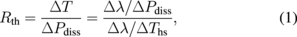
following the measurement of variations in the wavelength shift with changes in the dissipated power (Δλ/ΔPdiss) and with changes in the heat-sink temperature (Δλ/ΔThs).21–24) The reported Δλ/ΔThs values for GaN-based VCSELs range from 0.012 to 0.0185 nm/K.21,22,24,25) In this work, Δλ/ΔThs values were acquired under pulsed operation to prevent the thermal effect, and the results obtained for VCSELs with 5λ- and 10λ-cavity structures were 0.0142 and 0.0146 nm/K, respectively. These are comparable to the literature values. The Δλ/ΔPdiss values determined for the VCSELs having 5λ- and 10λ-cavity structures were 0.015 and 0.0103 nm/mW, respectively. Using Eq. (1), the Rth values were calculated to be 1100 and 710 K/W for the 5λ- and 10λ-cavity VCSELs, respectively. This 65% improvement indicates that the operating current at rollover in Figs. 2(a) and 2(b) was enhanced by a factor of approximately 1.5. As an example, the operating current at rollover was increased from 20 to 29 mA at 20 °C to give a ratio of 1.45. These results confirm that reducing Rth leads to a higher output power. Compared with the results of the theoretical analysis of the Rth values in Ref. 22, the impact of the Rth reduction was quite reasonable, indicating that a thicker n-GaN layer essentially improves the thermal dissipation in our VCSEL structure.22)
The internal temperatures at rollover ( ) were estimated to be 159 and 161 °C for the 5λ- and 10λ-cavity VCSELs using the respective Rth and dissipated power values at rollover. These similar
  values also suggest that the reduced Rth was the primary reason for the higher output power observed for the 10λ-cavity VCSEL. Thus, both
  and Rth are important with regard to establishing the maximum lasing temperature (
 ). Under the lasing condition, this temperature can be expressed as

where  is the dissipated power at the threshold, Ith is the threshold current, and Vth is the threshold voltage. Thus, the temperature dependence of Ith is also important in determining
  . Figure 4 shows plots of the effects of temperature on the threshold currents of the fabricated VCSELs. These data demonstrate that, over the temperature range from 293 to 333 K, the temperature dependence of Ith was minimal, and a relatively high characteristic temperature (T0 = 316 K) was obtained in the case of the 10λ-cavity VCSEL. In contrast, Ith rapidly increased with increasing temperature above 330 K. This tendency led to a significant internal temperature increase in the VCSELs below the threshold within the high-temperature region, resulting in the maximum lasing temperature of 110 °C observed for our device. The threshold current in VCSELs is governed by the mismatch between the wavelength of the cavity mode and the peak gain. Therefore, temperature-induced detuning of the lasing mode should be optimized in accordance with the requirements of each application.26)

Fig. 4. Temperature dependence of threshold current under CW operation.
Download figure:
Standard image High-resolution image
In conclusion, we have demonstrated the highest output power values (15.7 mW at 20 °C and 2.7 mW at 110 °C) yet obtained from a blue GaN-based VCSEL, as a result of introducing a long-cavity (10λ) structure and reducing the reflectivity (to 99.1%) of the front cavity mirror. Compared with a 5λ-cavity VCSEL, the thermal resistance was reduced from 1100 to 710 K/W. An analysis of thermal resistance revealed a high internal temperature of 434 K at the rollover point in these devices. This improvement, together with the adjusted reflectivity of the front mirror, led to superior performance, including a high output power of 15.7 mW, a differential efficiency of 31%, and a wall-plug efficiency of 8.9% at 20 °C, as well as a maximum CW operational temperature of 110 °C together with a significant output power of 2.7 mW. These results mark a major step toward establishing high-power GaN-based VCSELs.
Acknowledgments
The authors thank S. Tanaka, S. Kubo, K. Nakata, and K. Kiyohara for their support during the fabrication of the device and for helpful discussions. We also thank T. Tanabe and J. Sonoda for their encouragement during this work.