
Abstract
In this study, we investigated the effects of postmetallization annealing (PMA) on the interface properties of GaN metal–oxide–semiconductor (MOS) structures using Al2O3 prepared by atomic layer deposition. Excellent capacitance–voltage (C–V) characteristics without frequency dispersion were observed in the MOS sample after PMA in N2 ambient at 300–400 °C. The PMA sample showed state densities of only at most 4 × 1010 cm−1 eV−1. A geometric phase analysis of transmission electron microscopy images after PMA revealed a uniform distribution of the lattice constant near the Al2O3/GaN interface, leading to the improved bond termination and bonding order configuration along the interface.
Export citation and abstract BibTeX RIS

Content from this work may be used under the terms of the Creative Commons Attribution 4.0 license. Any further distribution of this work must maintain attribution to the author(s) and the title of the work, journal citation and DOI.
For reduced power consumption as well as failure protection, normally-off devices are highly preferred for power switching applications. Since normally-off transistors require a positive gate voltage to be turned on, a metal–insulator (oxide)–semiconductor (MIS or MOS) gate is absolutely necessary to suppress the forward gate current flow.1) In RF application, the 5G wireless system requires high efficiency and linearity for RF power transistors. Power amplifiers using Schottky-gate (SG) GaN high-electron-mobility transistors (HEMTs) suffer from reduced gain and efficiency with increasing input RF power owing to significant gate leakage currents caused by a large input swing that may drive the devices deep into the forward bias regime.2) Such high leakage currents seriously affect the operation stability and large signal linearity of power amplifiers. Moreover, a suitable surface passivation scheme is absolutely necessary for the stable and reliable operation of power devices. An MIS structure is very effective in overcoming such problems related to SG structures. In fact, Kanamura et al.2) demonstrated that gate leakage current was sufficiently controlled in the AlGaN/GaN MIS-HEMT even under high-input-power operation. Consequently, a MIS-HEMT can accommodate a wide range of input signal sweep, boosting a maximum output power.3–5)
Different insulator materials have been applied to GaN-based MIS structures.1) Since the semiconductor/insulator interfacial quality significantly affects the transistor performance, a chemically stable MIS structure with low interface state densities should be developed for practical device applications. To improve the interface properties of an MIS structure, postdeposition annealing (PDA) at high temperatures (800–1000 °C) has been the standard process. However, relatively high density electronic states remained at GaN MOS interfaces even after PDA.6,7) For MOS structures using Al2O3 and high-k materials, a limited process temperature should be considered. Hori et al.8) observed that the as-deposited Al2O3 layer has an amorphous-phase structure and that the Al2O3/GaN interface is uniformly flat. However, annealing at 800 °C generated a large number of microcrystallized regions in the Al2O3 layer, causing a marked increase in the leakage current of the Al2O3/GaN structure. The situation is even worse for HfO2 films where partial crystallization occurs at temperatures lower than 600 °C.9–11)
On the other hand, postmetallization annealing (PMA) at relatively low temperatures, which is the annealing process after gate metallization, has been applied to MIS structures using Si and compound semiconductors. Ma12) reported that the PMA treatment at 400 °C significantly reduced trap densities at Si3N4/Si interfaces. The PMA treatment at 400 °C was also found to be effective in improving the capacitance–voltage (C–V) characteristics of the TiO2/Al2O3/Si structure.13) Furthermore, Li et al.14) demonstrated that PMA at 300 °C in N2 enhanced gate controllability and transport properties in an InGaAs MOS-HEMT with Al2O3 as a gate oxide. As for GaN-based MOS structures, Hung et al.15) reported that the PMA treatment at temperatures varying from 400 to 550 °C mitigated the fluctuation of the flat-band voltage in C–V curves for Al2O3/GaN and Al2O3/AlGaN/GaN structures. However, the effects of PMA on the interface properties of GaN MOS structures are yet unclear. Accordingly, in this paper, we present the interface characterization of Al2O3/GaN structures prepared by atomic layer deposition (ALD) with and without PMA.
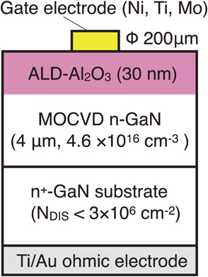
Figure 1 shows an Al2O3/n-GaN MOS structure prepared by ALD. We used a homoepitaxial Si-doped GaN layer of 4 µm thickness grown on an n+-GaN substrate with a relatively low dislocation density (<3 × 106 cm−2). The donor density is 4.6 × 1016 cm−3, which was extracted from the C–V characteristics of a Schottky diode fabricated on the same wafer. After the pretreatment of the n-GaN surface in 30% HF solution for 1 min, the Al2O3 layer with a nominal thickness of 30 nm was deposited on the n-GaN surface using an ALD system (SUGA-SAL1500) at 300 °C. In the deposition process, water vapor and trimethylaluminum were introduced into a reactor in alternate pulse forms. Each precursor was injected into the reactor for 15 ms, and the purging time was set to 5 s. In this case, the growth rate is 0.11 nm/cycle, indicating the formation of Al2O3 in a layer-by-layer fashion. From an ellipsometry measurement, the refractive index of the ALD Al2O3 was estimated to be 1.60–1.65, which is close to the values reported for amorphous Al2O3 films prepared by ALD.16) A gate electrode of 200 µm diameter was then formed on the Al2O3 surface. After the gate formation, we carried out PMA at 200–400 °C in N2.

Fig. 1. Schematic illustration of Al2O3/n-GaN MOS structure.
Download figure:
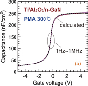
Standard image High-resolution imageFigure 2 shows the C–V characteristics of Ni/Al2O3/n-GaN diodes with and without PMA measured at room temperature. The as-deposited sample (without PMA) showed a significant frequency dispersion and a ledgelike feature at around the gate voltage (VG) of −3 V. By lowering the frequency of the ac measurement signal, deeper interface states are expected to respond accordingly to an ac signal. This allows more of the states to follow the ac frequency, contributing to an additional component to the measured capacitance. Similar frequency dispersions in C–V characteristics were reported for SiO2/GaN and Al2O3/GaN structures.17–19) In addition, decreased C–V slopes compared with that of the calculated curve (broken line) indicated the existence of interface states with a relatively high density. On the other hand, excellent C–V characteristics without frequency dispersion were observed in a very wide frequency range of 1 Hz to 1 MHz for the MOS sample after PMA in N2 at 300 °C for 10 min, as shown in Fig. 2. The PMA sample showed no ledgelike behavior with C–V curves very close to the calculated one, indicating that PMA realized the excellent Al2O3/GaN interface with low-density interface states. The difference in flat-band voltage (VFB) between samples without and with PMA is also evident in Fig. 2. Again, on one hand, the annealed sample exhibited a VFB very close to the calculated value; on the other hand, the as-deposited sample showed a VFB shift toward the negative bias direction, probably owing to excess positive charges arising from donor-type interface states and/or defect levels in the bulk Al2O3. A possible candidate for a defect level in Al2O3 is an oxygen-vacancy-related defect.20,21) PMA could decrease such a level, resulting in the VFB recovery toward the expected value. Hung et al.15) also reported a similar VFB recovery in Ni/Al2O3/GaN structures by PMA at 400–550 °C.
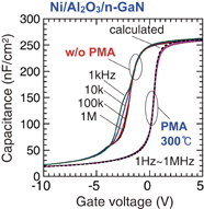
Fig. 2. C–V characteristics of Ni/Al2O3/n-GaN diodes with and without PMA measured at room temperature. PMA was carried out at 300 °C for 10 min in N2. The broken line indicates the calculated C–V curve.
Download figure:
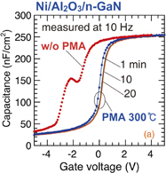
Standard image High-resolution imageFigures 3(a) and 3(b) respectively show the PMA time and temperature dependences of the C–V curves measured at 10 Hz. For PMA at 300 °C, the C–V behavior was improved even for a short annealing time of 1 min, as shown in Fig. 3(a). However, it was found from the differential coefficient of the C–V curve that the ledgelike feature remained at around VG = −0.5 V. Prolonging the treatment time to 10 min or longer realized the sufficient improvement of the C–V characteristics, i.e., no ledgelike feature with the C–V curves coinciding with the calculated one. In the case of PMA at 200 °C, we observed frequency dispersion in the low-frequency region, as shown in Fig. 3(b), suggesting the insufficient improvement of interface properties. On the other hand, PMA at 300 and 400 °C resulted in significantly improved C–V curves practically matching the calculated one, as shown in Fig. 3(b).
Download figure:
Standard image High-resolution image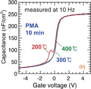
Fig. 3. Changes in C–V curves of Ni/Al2O3/n-GaN diodes measured at 10 Hz by varying the (a) PMA time and (b) temperature.
Download figure:
Standard image High-resolution imageFigure 4 shows the interface state density distributions of Al2O3/GaN interfaces. For the as-deposited sample, we applied the Terman method to the 1 MHz C–V result. High state densities in the order of 1012 cm−1 eV−1 were obtained for the sample without PMA. In addition, a peak corresponding to a density of 6 × 1012 cm−1 eV−1 appeared at around EC − 0.6 eV, probably arising from a discrete trap related to nitrogen-vacancy defects.22–24) On the other hand, PMA at 300–400 °C resulted in a significant reduction in state density. In fact, it was found that the interface state densities determined by the Terman method were below the detection limit (<1 × 1011 cm−2 eV−1). We then applied the conductance method to the PMA samples and obtained low state densities ranging from 1 to 4 × 1010 cm−2 eV−1 at energies near the conduction band edge, as shown in Fig. 4.
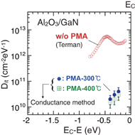
Fig. 4. Interface state density distributions of Al2O3/GaN interfaces without and with PMA. The Terman method was applied to the 1 MHz C–V result for the sample without PMA. On the other hand, state densities were extracted from the conductance method for the PMA samples.
Download figure:
Standard image High-resolution imageWe then investigated the effects of PMA on the Al2O3/GaN structures using different gate metals. Figure 5(a) shows the C–V curves of the Ti/Al2O3/GaN sample after PMA at 300 °C for 10 min in N2. Excellent C–V characteristics without frequency dispersion were observed, the same as with the Ni gate sample (Fig. 2). A similar result was observed in the MOS sample using Mo as a gate, indicating that the PMA effect can be observed in the Al2O3/GaN structures regardless of the gate metal used. The C–V curves at 1 MHz for the MOS structures using Ni, Ti, and Mo gate metals are summarized in Fig. 5(b). We clearly observed the parallel shift according to the difference in metal workfunction, like in a standard Si MOS structure, indicating a nearly ideal interface property of the Al2O3/GaN structures after PMA.
Download figure:
Standard image High-resolution image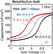
Fig. 5. (a) C–V curves in a wide frequency range of 1 Hz to 1 MHz for the Ti/Al2O3/GaN sample after PMA at 300 °C for 10 min in N2. The broken line indicates the calculated curve. (b) C–V curves measured at 1 MHz for MOS structures with PMA using Ni, Ti, and Mo gate metals. The number in each bracket indicates the metal workfunction.
Download figure:
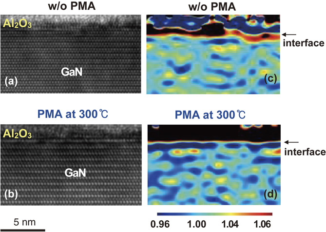
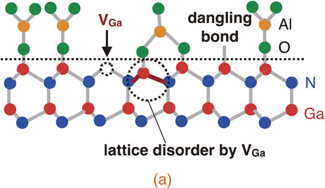
Standard image High-resolution imageFigures 6(a) and 6(b) show the high-resolution transmission electron microscopy (HRTEM) images of the Ni/Al2O3/GaN structures without and with PMA. For both images, periodic lattice points are clearly observed in the GaN layer. By the geometric phase analysis (GPA)25–27) of the HRTEM images, the relative lattice constants of GaN along the c-axis at the Al2O3/GaN interface were estimated. Maps of lattice constants along the c-axis relative to the ideal lattice constant of GaN (0.5186 nm) are shown in Figs. 6(c) and 6(d). Although a part of the amorphous Al2O3 layer near the interface is involved in this case, it should be noted that the values in the Al2O3 region are superficial because the GPA is only valid when applied to crystalline structures. The MOS sample without PMA showed a pronounced variation of lattice constants near the Al2O3/GaN interface, indicating the disorder in the atomic bonding configuration on the GaN surface. On an actual semiconductor surface, the termination of crystalline periodicity causes a peculiar bond configuration that includes dangling bonds and some kinds of surface reconstructions. In addition, the surface involves vacancies, adatoms, and natural oxides. Such surface irregularity induces lattice disorder in bond lengths and angles, as schematically shown in Fig. 7(a). For example, Xue et al.28) theoretically calculated the effect of Ga vacancy on the bond disorder at the Ga-polar GaN(0001) surface. They demonstrated that the electron transfer from the Ga dangling bond to the N dangling bond of a second layer N atom induced the downward relaxation of the neighboring Ga atom by 0.39 Å along the c-axis. For the Al2O3/GaN sample without PMA (as-deposited sample), the bond disorder at the GaN surface remained even after the Al2O3 deposition, leading to the pronounced variation of the lattice constants, as shown in Figs. 6(c) and 7(a). It is likely that such bond disorder is responsible for the poor C–V characteristics caused by high-density electronic states at the Al2O3/GaN interface.29,30)

Fig. 6. HRTEM images of the Ni/Al2O3/GaN structures (a) without and (b) with PMA. Maps of lattice constants along c-axis relative to ideal lattice constant of GaN for Ni/Al2O3/GaN structures (c) without and (b) with PMA.
Download figure:
Standard image High-resolution image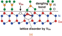
Download figure:
Standard image High-resolution image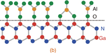
Fig. 7. Schematic models of atomic bonding configuration at Al2O3/GaN interfaces (a) before and (b) after PMA.
Download figure:
Standard image High-resolution image
As shown in Fig. 6(d), on the other hand, a uniform distribution of the lattice constant near the interface was observed for the sample with PMA at 300 °C for 10 min in N2. This indicates that PMA is effective for the termination of dangling bonds with O atoms and the relaxation of surface defects, as schematically shown in Fig. 7(b), leading to the improved bond termination and bonding order configuration at the Al2O3/GaN interface. The resulting reduction of the interface states brought excellent C–V characteristics without frequency dispersion in a very wide frequency range of 1 Hz to 1 MHz. Zywietz et al.31) predicted from theoretical calculations that the termination of Ga dangling bonds by O atoms effectively reduced the density of states (surface states) within the GaN bandgap.
In summary, we investigated the effects of PMA on the interface properties of ALD-Al2O3/GaN MOS structures using epitaxial n-GaN layers grown on a GaN substrate. The as-deposited sample showed a significant frequency dispersion and a ledgelike feature in C–V curves, showing high-density interface states in the range of 1012 cm−1 eV−1. On the other hand, excellent C–V characteristics without frequency dispersion were observed in the MOS sample after PMA in N2 at 300–400 °C for 10 min. The PMA sample showed state densities of at most 4 × 1010 cm−1 eV−1. The PMA effect was independent of the gate metal used in MOS structures, as evidenced by the parallel C–V shift according to the difference in metal workfunction. A geometric phase analysis of transmission electron microscopy images after PMA revealed a uniform distribution of the lattice constant near the Al2O3/GaN interface, leading to the improved bond termination and bonding order configuration along the interface. It is likely that the resulting reduction of the interface states afforded excellent C–V characteristics without frequency dispersion in a very wide frequency range of 1 Hz to 1 MHz. Finally, further study is warranted to gain deeper insight into the mechanism of bond ordering during PMA.
Acknowledgments
This work was partially support by JSPS KAKENHI Grant Number JP16H06421, Strategic International Collaborative Research Program (SICORP), Japan Science and Technology Agency (JST) and Council for Science, Technology and Innovation (CSTI).